
Document No. D16126EJ1V0DS00 (1st edition)
Date Published April 2002 N CP(K)
Printed in Japan
SILICON POWER TRANSISTOR
2SA1743
PNP SILICON EPITAXIAL TRANSISTOR
FOR HIGH-SPEED SWITCHING
DATA SHEET
The information in this document is subject to change without notice. Before using this document, please
confirm that this is the latest version.
Not all devices/types available in every country. Please check with local NEC representative for
availability and additional information.
©
2002
The 2SA1743 is a power transistor developed for high-speed
switching and features a high h
FE
at low V
CE(sat)
. This transistor is
ideal for use as a driver in DC/DC converters and actuators.
In addition, a small resin-molded insulation type package
contributes to high-density mounting and reduction of mounting
cost.
FEATURES
∑ High h
FE
and low V
CE(sat)
:
h
FE
100 (V
CE
=
-2 V, I
C
=
-2 A)
V
CE(sat)
0.3 V (I
C
=
-6 A, I
B
=
-0.3 A)
∑ Full-mold package that does not require an insulating board or
bushing
QUALITY GRADES
∑ Standard
Please refer to "Quality Grades on NEC Semiconductor Devices"
(Document No. C11531E) published by NEC Corporation to know
the specification of quality grade on the devices and its
recommended applications.
ABSOLUTE MAXIMUM RATINGS (Ta = 25
∞
∞
∞
∞C)
Parameter
Symbol
Ratings
Unit
Collector to base voltage
V
CBO
-100
V
Collector to emitter voltage
V
CEO
-60
V
Emitter to base voltage
V
EBO
-7.0
V
Collector current (DC)
I
C(DC)
-10
A
Collector current (pulse)
I
C(pulse)
*
-20
A
Base current (DC)
I
B(DC)
-5.0
A
Total power dissipation
P
T
(Tc = 25
∞C)
30
W
Total power dissipation
P
T
(Ta = 25
∞C)
2.0
W
Junction temperature
T
j
150
∞C
Storage temperature
T
stg
-55 to +150
∞C
PACKAGE DRAWING (UNIT: mm)
Electrode Connection
1. Base
2. Collector
3. Emitter
* PW
300
µs, duty cycle 10%
Data Sheet D16126EJ1V0DS
2
2SA1743
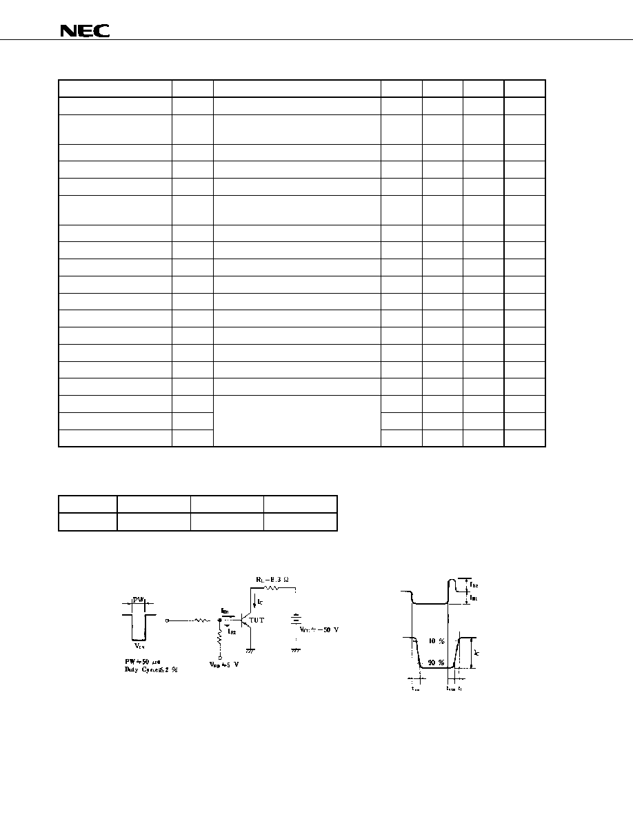
ELECTRICAL CHARACTERISTICS (Ta = 25
∞
∞
∞
∞C)
Parameter
Symbol
Conditions
MIN.
TYP.
MAX.
Unit
Collector to emitter voltage
V
CEO(SUS)
I
C
=
-6.0 A, I
B
=
-0.6 A, L = 1 mH
-60
V
Collector to emitter voltage
V
CEX(SUS)
I
C
=
-6.0 A, I
B1
=
-I
B2
=
-0.6 A,
V
BE(OFF)
= 1.5 V, L = 180
µH, clamped
-60
V
Collector cutoff current
I
CBO
V
CB
=
-60 V, I
E
= 0
-10
µA
Collector cutoff current
I
CER
V
CE
=
-60 V, R
BE
= 50
, Ta = 125∞C
-1.0
mA
Collector cutoff current
I
CEX1
V
CE
=
-60 V, V
BE(OFF)
= 1.5 V
-10
µA
Collector cutoff current
I
CEX2
V
CE
=
-60 V, V
BE(OFF)
= 1.5 V,
Ta = 125
∞C
-1.0
mA
Emitter cutoff current
I
EBO
V
EB
=
-5.0 V, I
C
= 0
-10
µA
DC current gain
h
FE1
*
V
CE
=
-2.0 V, I
C
=
-1.0 A
100
DC current gain
h
FE2
*
V
CE
=
-2.0 V, I
C
=
-2.0 A
100
400
DC current gain
h
FE3
*
V
CE
=
-2.0 V, I
C
=
-6.0 A
60
Collector saturation voltage
V
CE(sat)1
*
I
C
=
-6.0 A, I
B
=
-0.3 A
-0.3
V
Collector saturation voltage
V
CE(sat)2
*
I
C
=
-8.0 A, I
B
=
-0.4 A
-0.5
V
Base saturation voltage
V
BE(sat)1
*
I
C
=
-6.0 A, I
B
=
-0.3 A
-1.2
V
Base saturation voltage
V
BE(sat)2
*
I
C
=
-8.0 A, I
B
=
-0.4 A
-1.5
V
Collector capacitance
C
ob
V
CB
=
-10 V, I
E
= 0, f = 1.0 MHz
230
pF
Gain bandwidth product
f
T
V
CE
=
-10 V, I
C
=
-1.0 A
80
MHz
Turn-on time
t
on
0.3
µs
Storage time
t
stg
1.5
µs
Fall time
t
f
I
C
=
-6.0 A, R
L
= 8.3
,
I
B1
=
-I
B2
=
-0.3 A, V
CC
-50 V
Refer to the test circuit.
0.3
µs
* Pulse test PW
350
µs, duty cycle 2%
h
FE
CLASSIFICATION
Marking
M
L
K
h
FE2
100 to 200
150 to 300
200 to 400
SWITCHING TIME (t
on
, t
stg
, t
f
) TEST CIRCUIT
Base current
waveform
Collector current
waveform

Data Sheet D16126EJ1V0DS
3
2SA1743
TYPICAL CHARACTERISTICS (Ta = 25
∞
∞
∞
∞C)
T
o
t
a
l
P
o
w
e
r
Di
s
s
i
pa
t
i
on
P
T
(W)
Case Temperature T
C
(
∞C)
Collector to Emitter Voltage V
CE
(V)
Col
l
e
c
t
or Current
I
C
(
A
)
Col
l
e
c
t
or Current
I
C
(
A
)
Collector to Emitter Voltage V
CE
(V)
I
C
Derat
i
ng
dT
(%
)
Case Temperature T
C
(
∞C)
Single pulse
Trans
i
ent
Therm
a
l
Res
i
s
t
an
c
e
R
th
(
j
-
c)
(
∞
C/
W
)
Pulse Width PW (s)
Without heatsink
With infinite heatsink

