 | –≠–ª–µ–∫—Ç—Ä–æ–Ω–Ω—ã–π –∫–æ–º–ø–æ–Ω–µ–Ω—Ç: 2SC4228 | –°–∫–∞—á–∞—Ç—å:  PDF PDF  ZIP ZIP |

©
1993
DATA SHEET
SILICON TRANSISTOR
Document No. P10372EJ2V0DS00 (2nd edition)
(Previous No. TC-2404)
Date Published July 1995 P
Printed in Japan
2SC4228
DESCRIPTION
The 2SC4228 is a low supply voltage transistor designed for VHF,
UHF low noise amplifier.
It is suitable for a high density surface mount assembly since the
transistor has been applied super mini mold package.
This is achieved by direct nitride passivated base surface process
(NESAT
TM
process) which is an NEC proprietary fabrication technique.
FEATURES
∑
High f
T
: 8.0 GHz TYP. (@ V
CE
= 3 V, I
C
= 5 mA, f = 2 GHz)
∑
Low C
re
: 0.3 pF TYP. (@ V
CB
= 3 V, I
E
= 0, f = 1 MHz)
∑
High |S
21e
|
2
: 7.5 dB TYP. (@ V
CE
= 3 V, I
C
= 5 mA, f = 2 GHz)
∑
Super Mini Mold Package. (EIAJ: SC-70)
ORDERING INFORMATION
PART
QUANTITY
PACKING STYLE
NUMBER
2SC4228-T1
3 kpcs/Reel.
Embossed tape 8 mm wide.
Pin3 (Collector) face to perforation side
of the tape.
2SC4228-T2
3 kpcs/Reel.
Embossed tape 8 mm wide.
Pin1 (Emitter), Pin2 (Base) face to
perforation side of the tape.
*
Please contact with responsible NEC person, if you require evaluation
sample. Unit sample quantity shall be 50 pcs. (Part No.: 2SC4228)
HIGH FREQUENCY LOW NOISE AMPLIFIER
NPN SILICON EPITAXIAL TRANSISTOR
SUPER MINI MOLD
1.25 ± 0.1
2.1 ± 0.1
2.0 ± 0.2
0.3
≠0
+0.1
0.65
0.65
0.3
≠0
+0.1
2
1
3
0.9 ± 0.1
0.3
0.15
≠0.05
+0.1
0 to 0.1
Marking
PACKAGE DIMENSIONS
in millimeters
PIN CONNECTIONS
1.
2.
3.
Emitter
Base
Collector

2SC4228
2
ABSOLUTE MAXIMUM RATINGS (T
A
= 25 ∞C)
Collector to Base Voltage
V
CBO
20
V
Collector to Emitter Voltage
V
CEO
10
V
Emitter to Base Voltage
V
EBO
1.5
V
Collector Current
I
C
35
mA
Total Power Dissipation
P
T
150
mW
Junction Temperature
T
j
150
∞C
Storage Temperature
T
stg
≠65 to +150
∞C
ELECTRICAL CHARACTERISTICS (T
A
= 25 ∞C)
CHARACTERISTIC
SYMBOL
MIN.
TYP.
MAX.
UNIT
TEST CONDITIONS
Collector Cutoff Current
I
CBO
1.0
µ
A
V
CB
= 10 V, I
E
= 0
Emitter Cutoff Current
I
EBO
1.0
µ
A
V
EB
= 1 V, I
C
= 0
DC Current Gain
h
FE
50
100
250
V
CE
= 3 V, I
C
= 5 mA*
1
Gain Bandwidth Product
f
T
5.5
8.0
GHz
V
CE
= 3 V, I
C
= 5 mA, f = 2 GHz
Feedback Capacitance
C
re
0.3
0.7
pF
V
CB
= 3 V, I
E
= 0, f = 1 MHz*
2
Insertion Power Gain
|S
21e
|
2
5.5
7.5
dB
V
CE
= 3 V, I
C
= 5 mA, f = 2 GHz
Noise Figure
NF
1.9
3.2
dB
V
CE
= 3 V, I
C
= 5 mA, f = 2 GHz
*1 Pulse Measurement; PW
350
µ
s, Duty Cycle
2 %
*2 The emitter terminal and the case shall be connected to the guard terminal of the three-terminal capacitance
bridge.
h
FE
Classification
Rank
R43
R44
R45
Marking
R43
R44
R45
h
FE
50 to 100
80 to 160
125 to 250

2SC4228
3
TYPICAL CHARACTERISTICS (T
A
= 25 ∞C)
100
0
5
0
50
100
150
200
0.5
1.0
10
15
20
160 A
µ
140 A
µ
120 A
µ
100 A
µ
80 A
µ
60 A
µ
40 A
µ
I
B
= 20 A
µ
10
0.5
0
0.5
1.0
10
20
1
5
10
50
20
50
100
200
V
CE
= 3 V
V
CE
= 3 V
0.1
1
0
0.5
2
5
10
20
50
0.2
0.5
1.0
2.0
5.0
1
5
10
50
2
4
6
8
10
f = 1 MHz
V
CE
= 3 V
f = 2 GHz
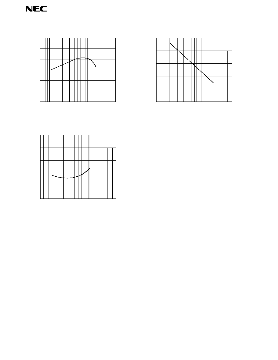
25
FEED-BACK CAPACITANCE vs.
COLLECTOR TO BASE VOLTAGE
COLLECTOR CURRENT vs.
BASE TO EMITTER VOLTAGE
DC CURRENT GAIN vs.
COLLECTOR CURRENT
TOTAL POWER DISSIPATION vs.
AMBIENT TEMPERATURE
COLLECTOR CURRENT vs.
COLLECTOR TO EMITTER VOLTAGE
GAIN BANDWIDTH PRODUCT vs.
COLLECTOR CURRENT
P
T
≠ Total Power Dissipation ≠ mW
I
C
≠ Collector Current ≠ mA
I
C
≠ Collector Current ≠ mA
h
FE
≠ DC Current Gain
C
re
≠ Feed-back Capacitance ≠ pF
f
T
≠ Gain Bandwidth Product ≠ GHz
T
A
≠ Ambient Temperature ≠ ∞C
V
CE
≠ Collector to Emitter Voltage ≠ V
V
BE
≠ Base to Emitter Voltage ≠ V
I
C
≠ Collector Current ≠ mA
V
CB
≠ Collector to Base Voltage ≠ V
I
C
≠ Collector Current ≠ mA
Free Air
2SC4228
4
0
0.5
0
0.5
1
5
10
50
4
8
12
0.1
1.0
0.5
5.0
0
5
10
15
20
25
1
5
10
50
1
2
3
4
5
V
CE
= 3 V
f = 2 GHz
V
CE
= 3 V
I
C
= 5 mA
V
CE
= 3 V
f = 2 GHz
|S
21e
|
2
≠ Insertion Power Gain ≠ dB
I
C
≠ Collector Current ≠ mA
f ≠ Frequency ≠ GHz
|S
21e
|
2
≠ Insertion Power Gain ≠ dB
I
C
≠ Collector Current ≠ mA
NF ≠ Noise Figure ≠ dB
INSERTION POWER GAIN vs.
COLLECTOR CURRENT
INSERTION POWER GAIN vs.
FREQUENCY
NOISE FIGURE vs.
COLLECTOR CURRENT

2SC4228
5
S-PARAMETER
V
CE
= 3 V, I
C
= 5 mA, Z
O
= 50
FREQUENCY
S11
S21
S12
S22
MHz
MAG
ANG
MAG
ANG
MAG
ANG
MAG
ANG
100.00
.875
≠18.6
14.087
161.1
.018
78.2
.958
≠10.1
200.00
.762
≠35.0
12.290
145.1
.034
68.6
.888
≠17.7
300.00
.677
≠47.2
10.888
133.6
.048
66.6
.800
≠24.4
400.00
.565
≠59.4
9.275
123.6
.055
65.8
.719
≠26.7
500.00
.495
≠67.5
8.300
115.7
.063
63.5
.669
≠28.7
600.00
.425
≠76.1
7.184
108.9
.074
61.1
.610
≠30.3
700.00
.372
≠81.6
6.454
104.8
.084
63.8
.600
≠30.6
800.00
.327
≠88.5
5.818
99.5
.089
62.7
.560
≠31.3
900.00
.289
≠93.6
5.231
95.5
.092
64.6
.543
≠30.1
1000.00
.255
≠100.5
4.820
92.0
.104
62.8
.519
≠33.4
1100.00
.236
≠105.2
4.444
88.8
.105
64.2
.512
≠31.8
1200.00
.214
≠112.2
4.142
85.3
.113
64.2
.497
≠33.4
1300.00
.195
≠117.6
3.842
83.2
.122
63.6
.476
≠33.2
1400.00
.182
≠123.8
3.554
79.3
.127
65.0
.481
≠34.2
1500.00
.165
≠129.9
3.343
77.4
.139
64.1
.467
≠34.6
1600.00
.153
≠137.4
3.218
75.3
.140
64.5
.466
≠34.8
1700.00
.145
≠144.3
3.091
73.6
.152
65.4
.458
≠37.2
1800.00
.139
≠151.8
2.857
70.4
.162
64.3
.456
≠36.1
1900.00
.134
≠157.0
2.764
68.7
.168
62.3
.451
≠38.4
2000.00
.129
≠164.7
2.624
66.4
.176
64.8
.445
≠39.0
V
CE
= 3 V, I
C
= 3 mA, Z
O
= 50
FREQUENCY
S11
S21
S12
S22
MHz MAG
ANG
MAG
ANG
MAG
ANG
MAG
ANG
100.00
.943
≠13.4
9.384
165.9
.020
84.1
.969
≠7.7
200.00
.868
≠26.6
8.668
152.8
.038
77.2
.936
≠13.8
300.00
.815
≠37.7
8.165
142.9
.051
67.9
.876
≠20.9
400.00
.717
≠48.9
7.279
132.9
.062
63.9
.804
≠23.5
500.00
.655
≠56.8
6.780
125.5
.075
63.9
.764
≠26.7
600.00
.577
≠65.5
6.061
118.0
.084
60.0
.708
≠29.7
700.00
.518
≠71.2
5.504
112.8
.091
59.7
.685
≠31.1
800.00
.468
≠78.1
5.074
106.7
.098
57.0
.639
≠32.0
900.00
.420
≠83.7
4.632
102.8
.102
59.0
.611
≠32.8
1000.00
.380
≠90.6
4.340
98.3
.105
56.6
.592
≠35.0
1100.00
.344
≠94.8
3.951
94.8
.112
57.8
.579
≠34.1
1200.00
.321
≠101.6
3.717
90.5
.121
59.0
.551
≠35.0
1300.00
.291
≠105.9
3.485
87.6
.128
58.7
.532
≠35.9
1400.00
.273
≠111.7
3.306
84.3
.135
59.8
.535
≠36.6
1500.00
.250
≠117.2
3.134
80.7
.140
58.0
.511
≠37.5
1600.00
.228
≠122.4
2.959
79.0
.145
59.5
.516
≠37.7
1700.00
.219
≠128.5
2.819
76.0
.153
59.0
.504
≠39.0
1800.00
.199
≠135.3
2.699
73.9
.161
58.4
.493
≠39.9
1900.00
.193
≠139.6
2.572
71.9
.163
60.3
.489
≠41.4
2000.00
.182
≠146.9
2.474
68.3
.175
59.8
.482
≠41.4