 | –≠–ª–µ–∫—Ç—Ä–æ–Ω–Ω—ã–π –∫–æ–º–ø–æ–Ω–µ–Ω—Ç: 2SC4336 | –°–∫–∞—á–∞—Ç—å:  PDF PDF  ZIP ZIP |

The information in this document is subject to change without notice. Before using this document, please
confirm that this is the latest version.
Not all products and/or types are available in every country. Please check with an NEC Electronics
sales representative for availability and additional information.
SILICON POWER TRANSISTOR
2SC4336
NPN SILICON EPITAXIAL TRANSISTOR
FOR HIGH-SPEED SWITCHING
DATA SHEET
Document No. D17261EJ1V0DS00 (1st edition)
Date Published July 2004 NS CP(K)
Printed in Japan
2004
DESCRIPTION
The 2SC4336 is a mold power transistor developed for high-
speed switching and features a very low collector-to-emitter
saturation. This transistor is ideal for use in switching power
supplies, DC/DC converters, motor drivers, solenoid drivers, and
other low-voltage power supply devices, as well as for high-current
switching.
FEATURES
∑ Mold package that does not require an insulating board or
insulation bushing
∑ Fast switching speed
∑ Low collector-to-emitter saturation voltage
V
CE(sat)
0.3 V MAX. (I
C
= 6.0 A)
ORDERING INFORMATION
PART NUMBER
PACKAGE
2SC4336 Isolated
TO-220
(MP-45)
ABSOLUTE MAXIMUM RATINGS (T
A
= 25∞C)
Collector to base voltage
V
CBO
100 V
Collector to emitter voltage
V
CEO
100 V
Emitter to base voltage
V
EBO
7.0 V
Collector current (DC)
I
C(DC)
10 A
Collector current (pulse)
Note
I
C(pulse)
20 A
Base current (DC)
I
B(DC)
6.0 A
Total power dissipation (T
C
= 25
∞C) P
T
30 W
Total power dissipation (T
A
= 25
∞C) P
T
2.0
W
Junction temperature
T
j
150
∞C
Storage temperature
T
stg
-55 to +150
∞C
Note PW
300
µ
s, Duty Cycle
10%
PACKAGE DRAWING (Unit: mm)
10.5 MAX.
7 ±0.2
3.2 ±0.2
3.0 MAX.
1.3 ±0.2
0.8 ±0.1
2.54 TYP.
2.54 TYP.
1.5 ±0.2
5 ±0.2
13.5 MIN.
12 ±0.2
5
±0.1
17 ±0.2
2.8 ±0.2
4.7 MAX.
2.5 ±0.1
0.5 ±0.1
1 2 3
1: Base
2: Collector
3: Emitter

Data Sheet D17261EJ1V0DS
2
2SC4336
ELECTRICAL CHARACTERISTICS (T
A
= 25∞C)
Parameter Symbol
Conditions
MIN.
TYP.
MAX.
Unit
Collector to Emitter Voltage
V
CEO(SUS)
I
C
= 5.0 A, I
B
= 0.6 A, L = 1 mH
100
V
V
CEX(SUS)
I
C
= 5.0 A, I
B1
=
-I
B2
= 0.6 A,
V
BE(OFF)
=
-1.5 V,
L = 180
µ
H, clamped
100 V
Collector Cut-off Current
I
CBO
V
CB
= 100 V, I
E
= 0
10
µ
A
I
CER
V
CE
= 100 V, R
BE
= 50
, T
A
= 125
∞C 1.0 mA
I
CEX1
V
CE
= 100 V, V
BE(OFF)
=
-1.5 V
10
µ
A
I
CEX2
V
CE
= 100 V, V
BE(OFF)
=
-1.5 V,
T
A
= 125
∞C
1.0
mA
Emitter Cut-off Current
I
EBO
V
EB
= 5.0 V, I
C
= 0
10
µ
A
DC Current Gain
Note
h
FE1
V
CE
= 2.0 V, I
C
= 1.0 A
100
h
FE2
V
CE
= 2.0 V, I
C
= 2.0 A
100
200
400
h
FE3
V
CE
= 2.0 V, I
C
= 6.0 A
60
Collector Saturation Voltage
Note
V
CE(sat)1
I
C
= 6.0 A, I
B
= 0.3 A
0.3
V
V
CE(sat)2
I
C
= 8.0 A, I
B
= 0.4 A
0.5
V
Base Saturation Voltage
Note
V
BE(sat)1
I
C
= 6.0 A, I
B
= 0.3 A
1.2
V
V
BE(sat)2
I
C
= 8.0 A, I
B
= 0.4 A
1.5
V
Collector Capacitance
C
ob
V
CB
= 10 V, I
E
= 0, f = 1.0 MHz
120
pF
Gain Bandwidth Product
f
T
V
CE
= 10 V, I
C
= 0.5 A
150
MHz
Turn-on Time
t
on
0.3
µ
s
Storage Time
t
stg
1.5
µ
s
Fall Time
t
f
I
C
= 6.0 A, R
L
= 8.3
,
I
B1
=
-I
B2
= 0.3 A, V
CC
50 V
Refer to the test circuit.
0.3
µ
s
Note Pulsed: PW
350
µ
s, Duty Cycle
2%
h
FE
CLASSIFICATION
Marking M
L
K
h
FE2
100 to 200
150 to 300
200 to 400
SWITCHING TIME (t
on
, t
stg
, t
f
) TEST CIRCUIT
V
CC
50 V
R
L
= 8.3
I
B1
I
B2
I
C
I
C
T.U.T.
V
IN
PW
PW
50 s
V
BB
-5 V
Duty Cycle
2%
t
on
t
stg
t
f
90%
I
B1
I
B2
10%
Base current
waveform
Collector current
waveform
µ

Data Sheet D17261EJ1V0DS
3
2SC4336
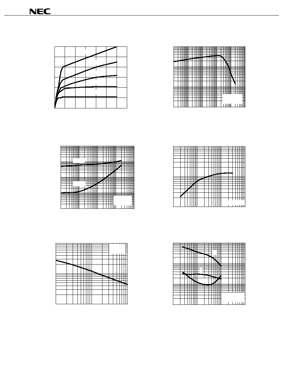
TYPICAL CHARACTERISTICS (T
A
= 25∞C)
TOTAL POWER DISSIPATION vs.
CASE TEMPERATURE
DERATING CURVE OF SAFE OPERATING AREA
P
T
- Total Powe
r
Dissipation - W
0
5
10
15
20
25
30
0
25
50
75
100 125 150 175
T
C
- Case Temperature -
∞C
dT - Pe
rcentage
of Rated Powe
r -
%
0
20
40
60
80
100
0
25
50
75
100
125
150
S/b Limited
Dissipation Limited
T
C
- Case Temperature -
∞C
FORWARD BIAS SAFE OPERATING AREA
I
C
- Collector Cu
r
r
ent - A
0.01
0.1
1
10
100
0.1
1
10
100
1000
I
C(pulse)
I
C(DC)
Single pulse
T
C
= 25∞C
1 ms
10 ms
200 ms
DC Dissipation Limited
V
CE
- Collector to Emittor Voltage - V
TRANSIENT THERMAL RESISTANCE vs. PULSE WIDTH
R
th
(j
-c)
- T
r
ansient Thermal Resistance -
∞
C/W
0.1
1
10
100
1000
R
th(ch-A)
= 62.5∞C/W
R
th(ch-C)
= 4.17∞C/W
Single pulse
PW - Pulse Width - s
1 m
10 m
100 m
1
10
100
1000
Data Sheet D17261EJ1V0DS
4
2SC4336
COLLECTOR CURRENT vs.
COLLECTOR TO EMITTER VOLTAGE
DC CURRENT GAIN vs.
COLLECTOR CURRENT
I
C
- Collector Cu
r
r
ent - A
0
2
4
6
8
10
12
0
0.5
1
1.5
2
2.5
3
3.5
I
B
= 10 mA
20 mA
30 mA
50 mA
100 mA
V
CE
- Collector to Emittor Voltage - V
h
FE
- D
C
Cu
rrent
Gai
n
1
10
100
1000
0.001
0.01
0.1
1
10
100
V
CE
= 2.0 V
Pulsed
I
C
- Collector Current - A
COLLECTOR SATURATION VOLTAGE AND BASE
SATURATION VOLTAGE vs. COLLECTOR CURRENT
GAIN BANDWIDTH PRODUCT vs.
COLLECTOR
CURRENT
V
CE
-
Collector Saturation Voltag
e - mV
V
BE
- Base Sat
u
ration Voltage -
mV
1
10
100
1000
10000
0.01
0.1
1
10
100
I
C
= 10
∑ I
B
Pulsed
V
BE(sat)
V
CE(sat)
I
C
- Collector Current - A
f
T
- Gain Band
width Product -
MHz
10
100
1000
0.01
0.1
1
10
V
CE
= 10 V
I
C
- Collector Current - A
COLLECTOR CAPACITANCE vs.
COLLECTOR TO BASE VOLTAGE
TURN ON TIME, STORAGE TIME AND FALL TIME
vs. COLLECTOR CURRENT
C
ob
-
C
o
llector Capacitance - pF
10
100
1000
1
10
100
I
E
= 0
f = 1 MHz
V
CB
- Collector to Base Voltage - V
t
f
,
t
st
g
, t
on
- Fall Tim
e
, Turn-on Time a
nd Storage Time -
ns
10
100
1000
10000
0.1
1
10
100
I
C
= 20 A
I
B1
=
-20 ∑ I
B2
t
on
t
stg
t
f
I
C
- Collector Current - A
2SC4336
The information in this document is current as of July, 2004. The information is subject to change
without notice. For actual design-in, refer to the latest publications of NEC Electronics data sheets or
data books, etc., for the most up-to-date specifications of NEC Electronics products. Not all
products and/or types are available in every country. Please check with an NEC Electronics sales
representative for availability and additional information.
No part of this document may be copied or reproduced in any form or by any means without the prior
written consent of NEC Electronics. NEC Electronics assumes no responsibility for any errors that may
appear in this document.
NEC Electronics does not assume any liability for infringement of patents, copyrights or other intellectual
property rights of third parties by or arising from the use of NEC Electronics products listed in this document
or any other liability arising from the use of such products. No license, express, implied or otherwise, is
granted under any patents, copyrights or other intellectual property rights of NEC Electronics or others.
Descriptions of circuits, software and other related information in this document are provided for illustrative
purposes in semiconductor product operation and application examples. The incorporation of these
circuits, software and information in the design of a customer's equipment shall be done under the full
responsibility of the customer. NEC Electronics assumes no responsibility for any losses incurred by
customers or third parties arising from the use of these circuits, software and information.
While NEC Electronics endeavors to enhance the quality, reliability and safety of NEC Electronics products,
customers agree and acknowledge that the possibility of defects thereof cannot be eliminated entirely. To
minimize risks of damage to property or injury (including death) to persons arising from defects in NEC
Electronics products, customers must incorporate sufficient safety measures in their design, such as
redundancy, fire-containment and anti-failure features.
NEC Electronics products are classified into the following three quality grades: "Standard", "Special" and
"Specific".
The "Specific" quality grade applies only to NEC Electronics products developed based on a customer-
designated "quality assurance program" for a specific application. The recommended applications of an NEC
Electronics product depend on its quality grade, as indicated below. Customers must check the quality grade of
each NEC Electronics product before using it in a particular application.
The quality grade of NEC Electronics products is "Standard" unless otherwise expressly specified in NEC
Electronics data sheets or data books, etc. If customers wish to use NEC Electronics products in applications
not intended by NEC Electronics, they must contact an NEC Electronics sales representative in advance to
determine NEC Electronics' willingness to support a given application.
(Note)
∑
∑
∑
∑
∑
∑
M8E 02. 11-1
(1)
(2)
"NEC Electronics" as used in this statement means NEC Electronics Corporation and also includes its
majority-owned subsidiaries.
"NEC Electronics products" means any product developed or manufactured by or for NEC Electronics (as
defined above).
Computers, office equipment, communications equipment, test and measurement equipment, audio
and visual equipment, home electronic appliances, machine tools, personal electronic equipment
and industrial robots.
Transportation equipment (automobiles, trains, ships, etc.), traffic control systems, anti-disaster
systems, anti-crime systems, safety equipment and medical equipment (not specifically designed
for life support).
Aircraft, aerospace equipment, submersible repeaters, nuclear reactor control systems, life
support systems and medical equipment for life support, etc.
"Standard":
"Special":
"Specific":