 | –≠–ª–µ–∫—Ç—Ä–æ–Ω–Ω—ã–π –∫–æ–º–ø–æ–Ω–µ–Ω—Ç: 2SJ647 | –°–∫–∞—á–∞—Ç—å:  PDF PDF  ZIP ZIP |
The information in this document is subject to change without notice. Before using this document, please
confirm that this is the latest version.
Not all products and/or types are available in every country. Please check with an NEC Electronics
sales representative for availability and additional information.
MOS FIELD EFFECT TRANSISTOR
2SJ647
P-CHANNEL MOS FIELD EFFECT TRANSISTOR
FOR SWITCHING
DATA SHEET
Document No.
D16530EJ1V0DS00 (1st edition)
Date Published
January 2003 NS CP(K)
Printed in Japan
2003
DESCRIPTION
The 2SJ647 is a switching device which can be driven directly
by a 2.5 V power source.
The 2SJ647 features a low on-state resistance and excellent
switching characteristics, and is suitable for applications such
as power switch of portable machine and so on.
FEATURES
∑
2.5 V drive available
∑
Low on-state resistance
R
DS(on)1
= 1.45
MAX. (V
GS
=
-
4.5 V, I
D
=
-
0.2 A)
R
DS(on)2
= 1.55
MAX. (V
GS
=
-
4.0 V, I
D
=
-
0.2 A)
R
DS(on)3
= 2.98
MAX. (V
GS
=
-
2.5 V, I
D
=
-
0.15 A)
ORDERING INFORMATION
PART NUMBER
PACKAGE
2SJ647
SC-70 (SSP)
Remark Marking: H22
ABSOLUTE MAXIMUM RATINGS (T
A
= 25∞C)
Drain to Source Voltage (V
GS
= 0 V)
V
DSS
-
20
V
Gate to Source Voltage (V
DS
= 0 V)
V
GSS
m
12
V
Drain Current (DC) (T
A
= 25∞C)
I
D(DC)
m
0.4
A
Drain Current (pulse)
Note1
I
D(pulse)
m
1.6
A
Total Power Dissipation
Note2
P
T
0.2
W
Channel Temperature
T
ch
150
∞C
Storage Temperature
T
stg
-
55 to +150
∞C
Notes 1. PW
10
µ
s, Duty Cycle
1%
2. Mounted on FR-4 board of 2500 mm
2
x 1.1 mm.
Remark
The diode connected between the gate and source of the transistor serves as a protector against ESD. When
this device actually used, an additional protection circuit is externally required if a voltage exceeding the rated
voltage may be applied to this device.
Caution This product is electrostatic-sensitive device due to low ESD capability and should be handled with
caution for electrostatic discharge.
V
ESD
±100 V TYP. at C = 200 pF, R = 0, Single Pulse.
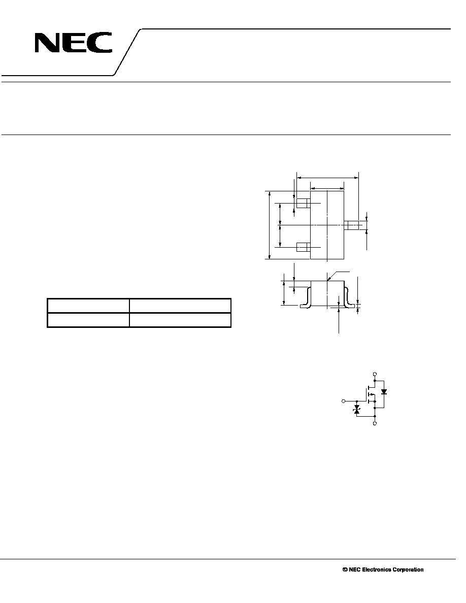
PACKAGE DRAWING (Unit: mm)
2.1 ± 0.1
1.25 ± 0.1
0.65
0.3
0.65
2.0 ± 0.2
0.9 ± 0.1
0 to 0.1
0.15
+0.1 ≠0.05
2
1
3
+0.1 ≠0
0.3
+0.1 ≠0
0.3
Marking
1 : Source
2 : Gate
3 : Drain
EQUIVALENT CIRCUIT
Source
Body
Diode
Gate
Protection
Diode
Gate
Drain
Data Sheet D16530EJ1V0DS
2
2SJ647
ELECTRICAL CHARACTERISTICS (T
A
= 25∞C)
CHARACTERISTICS
SYMBOL
TEST CONDITIONS
MIN.
TYP.
MAX.
UNIT
Zero Gate Voltage Drain Current
I
DSS
V
DS
=
-
20 V, V
GS
= 0 V
-
1.0
µ
A
Gate Leakage Current
I
GSS
V
GS
=
m
12 V, V
DS
= 0 V
m
10
µ
A
Gate Cut-off Voltage
V
GS(off)
V
DS
=
-
10 V, I
D
=
-
1.0
mA
-
0.8
-
1.3
-
1.8
V
Forward Transfer Admittance
| y
fs
|
V
DS
=
-
10 V, I
D
=
-
0.2 A
0.2
0.6
S
Drain to Source On-state Resistance
R
DS(on)1
V
GS
=
-
4.5 V, I
D
=
-
0.2 A
1.17
1.45
R
DS(on)2
V
GS
=
-
4.0 V, I
D
=
-
0.2 A
1.25
1.55
R
DS(on)3
V
GS
=
-
2.5 V, I
D
=
-
0.15 A
2.25
2.98
Input Capacitance
C
iss
V
DS
= ≠10 V
29
pF
Output Capacitance
C
oss
V
GS
= 0 V
15
pF
Reverse Transfer Capacitance
C
rss
f = 1.0 MHz
3
pF
Turn-on Delay Time
t
d(on)
V
DD
=
-
10 V, I
D
=
-
0.2 A
23
ns
Rise Time
t
r
V
GS
=
-
4.0 V
39
ns
Turn-off Delay Time
t
d(off)
R
G
= 10
50
ns
Fall Time
t
f
33
ns
Body Diode Forward Voltage
V
F(S-D)
I
F
= 0.4 A, V
GS
= 0 V
0.93
V
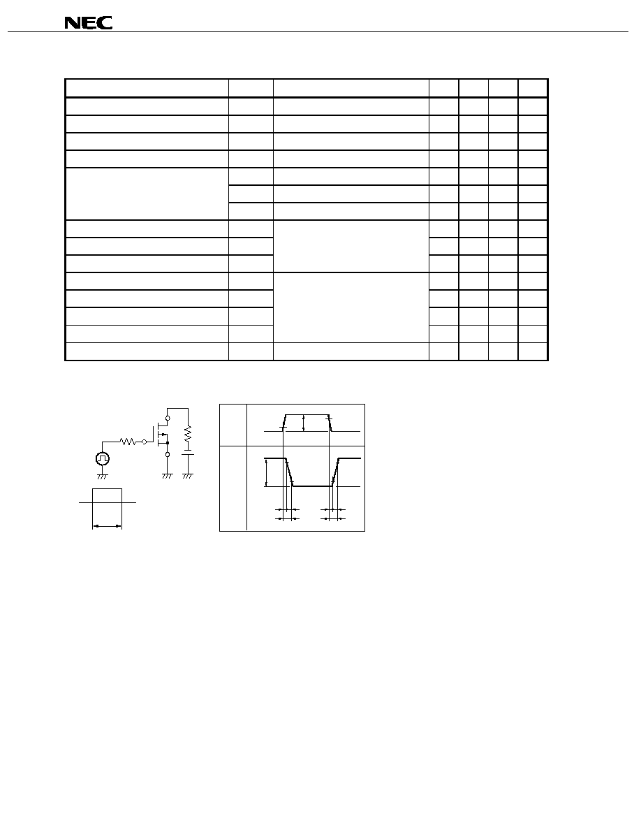
TEST CIRCUIT SWITCHING TIME
PG.
R
G
0
V
GS (
-
)
D.U.T.
R
L
V
DD
= 1 s
µ
Duty Cycle
1%
V
GS
Wave Form
V
DS
Wave Form
V
GS(
-
)
V
DS(
-
)
10%
0
0
90%
90%
90%
V
GS
V
DS
t
on
t
off
t
d(on)
t
r
t
d(off)
t
f
10%
10%

Data Sheet D16530EJ1V0DS
3
2SJ647
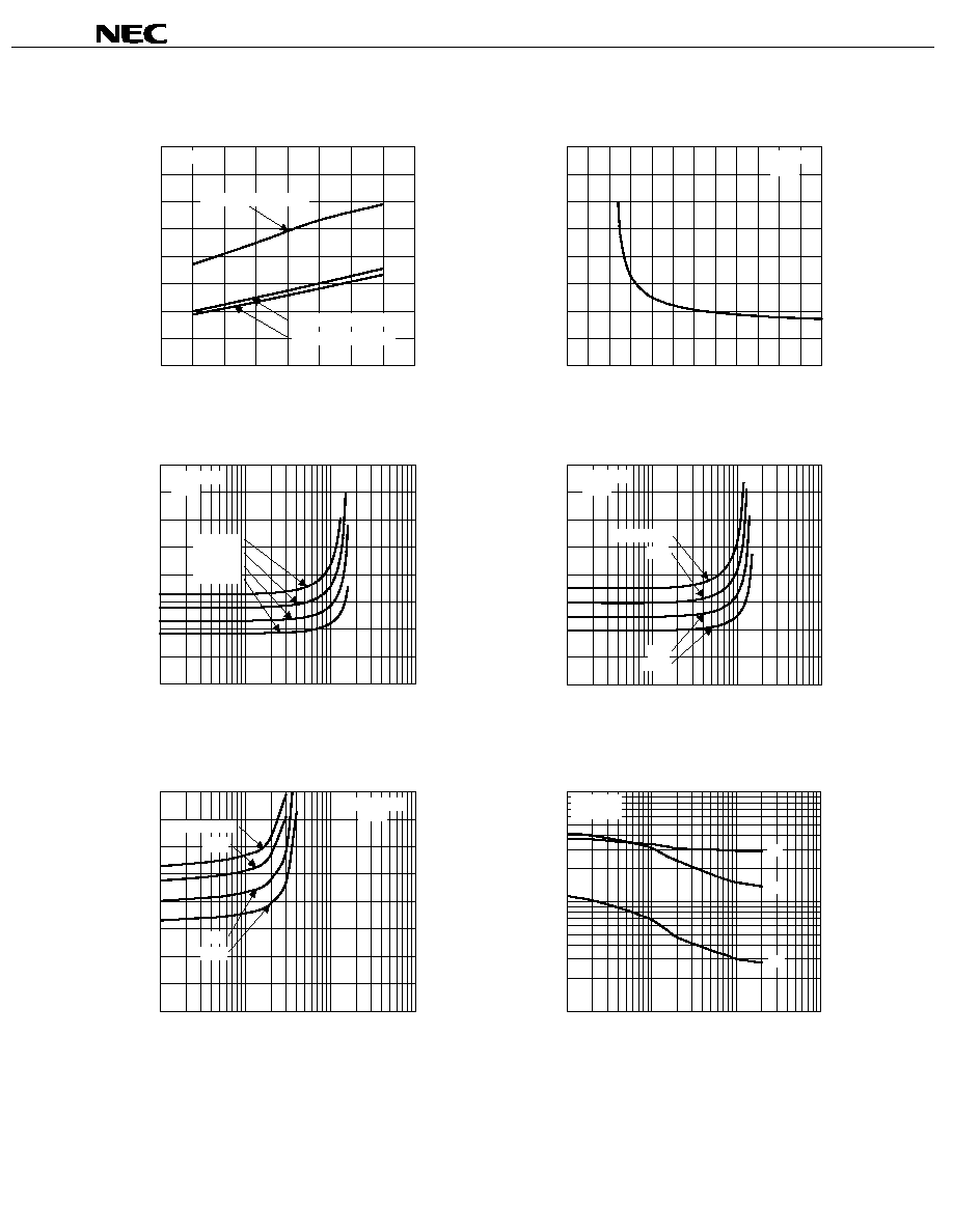
TYPICAL CHARACTERISTICS (T
A
= 25∞C)
DERATING FACTOR OF FORWARD BIAS
SAFE OPERATING AREA
TOTAL POWER DISSIPATION vs.
AMBIENT TEMPERATURE
dT - P
e
rc
ent
age of
Rat
ed P
o
w
e
r - %
0
20
40
60
80
100
120
0
25
50
75
100
125
150
175
P
T
-
T
o
ta
l
Po
w
e
r
D
i
ssi
p
at
i
on - W
0
0.04
0.08
0.12
0.16
0.2
0.24
0
25
50
75
100
125
150
175
Mounted on FR-4 board of
2500 mm
2
x 1.1 mm
T
A
- Ambient Temperature -
∞
C
T
A
- Ambient Temperature -
∞
C
DRAIN CURRENT vs.
DRAIN TO SOURCE VOLTAGE
FORWARD TRANSFER CHARACTERISTICS
I
D
- Drai
n Current
- A
0
-0.4
-0.8
-1.2
-1.6
0
-1
-2
-3
-4
-5
Pulsed
-
2.5 V
V
GS
=
-
4.5 V
-
4.0 V
I
D
- Drai
n Current
- A
-0.0001
-0.001
-0.01
-0.1
-1
-10
0
-1
-2
-3
-4
V
DS
=
-
10 V
Pulsed
T
A
= 125∞C
75∞C
25∞C
-
25∞C
V
DS
- Drain to Source Voltage - V
V
GS
- Gate to Source Voltage - V
GATE CUT-OFF VOLTAGE vs.
CHANNEL TEMPERATURE
FORWARD TRANSFER ADMITTANCE vs.
DRAIN CURRENT
-0.6
-0.8
-1
-1.2
-1.4
-1.6
-50
0
50
100
150
V
DS
=
-
10 V
I
D
=
-
1.0 mA
0.01
0.1
1
10
-0.001
-0.01
-0.1
-1
-10
T
A
=
-
25∞C
25∞C
75∞C
125∞C
V
DS
=
-
10 V
Pulsed
V
G
S
(
o
ff)
- Gat
e
Cut
-
of
f
V
o
l
t
age - V
T
ch
≠ Channel Temperrature -
∞
C
| y
fs
| - Forw
ard Trans
f
e
r A
d
m
i
t
t
anc
e - S
I
D
- Drain Current - A
Data Sheet D16530EJ1V0DS
4
2SJ647
DRAIN TO SOURCE ON-STATE RESISTANCE vs.
CHANNEL TEMPERATURE
DRAIN TO SOURCE ON-STATE RESISTANCE vs.
GATE TO SOURCE VOLTAGE
R
DS
(
on
)
- Drai
n t
o
S
ourc
e
On-s
t
a
t
e
Res
i
s
t
anc
e -
0
1
2
3
4
-50
0
50
100
150
Pulsed
V
GS
=
-
2.5 V, I
D
=
-
0.15 A
V
GS
=
-
4.0 V, I
D
=
-
0.2 A
V
GS
=
-
4.5 V, I
D
=
-
0.2 A
R
DS
(
on
)
- Drai
n t
o
S
ourc
e
On-s
t
a
t
e
Res
i
s
t
anc
e -
0
1
2
3
4
0
-2
-4
-6
-8
-10
-12
Pulsed
I
D
=
-
0.2 A
T
ch
≠ Channel Temperrature -
∞
C
V
GS
- Gate to Source Voltage - V
DRAIN TO SOURCE ON-STATE RESISTANCE vs.
DRAIN CURRENT
DRAIN TO SOURCE ON-STATE RESISTANCE vs.
DRAIN CURRENT
R
DS
(
on
)
- Drai
n t
o
S
ourc
e
On-s
t
a
t
e
Res
i
s
t
anc
e -
0
1
2
3
4
-0.01
-0.1
-1
-10
V
GS
=
-
4.5 V
Pulsed
T
A
= 125∞C
75∞C
25∞C
-
25∞C
R
DS
(
on
)
- Drai
n t
o
S
ourc
e
On-s
t
a
t
e
Res
i
s
t
anc
e -
0
1
2
3
4
-0.01
-0.1
-1
-10
V
GS
=
-
4.0 V
Pulsed
-
25∞C
25∞C
75∞C
T
A
= 125∞C
I
D
- Drain Current - A
I
D
- Drain Current - A
DRAIN TO SOURCE ON-STATE RESISTANCE vs.
DRAIN CURRENT
CAPACITANCE vs.
DRAIN TO SOURCE VOLTAGE
0
1
2
3
4
-0.01
-0.1
-1
-10
V
GS
=
-
2.5 V
Pulsed
-
25∞C
25∞C
75∞C
T
A
= 125∞C
1
10
100
-0.1
-1
-10
-100
V
GS
= 0 V
f = 1.0 MHz
C
iss
C
oss
C
rss
R
DS
(
on)
- Drai
n t
o
S
ourc
e
On-s
t
a
t
e
Res
i
s
t
anc
e - m
I
D
- Drain Current - A
C
is
s
, C
os
s
, C
rs
s
- Capac
i
t
anc
e ≠ pF
V
DS
- Drain to Source Voltage - V

Data Sheet D16530EJ1V0DS
5
2SJ647
SWITCHING CHARACTERISTICS
SOURCE TO DRAIN DIODE FORWARD VOLTAGE
t
d(
on)
, t
r
, t
d(
of
f
)
, t
f
- S
w
i
t
c
h
i
ng Ti
m
e
≠ ns
10
100
1000
-0.01
-0.1
-1
-10
V
DD
=
-
10 V
V
GS
=
-
4.0 V
R
G
= 10
t
d(off)
t
d(on)
t
f
t
r
I
F
≠ Di
ode Forw
ard Current
- A
0.001
0.01
0.1
1
10
0.4
0.6
0.8
1
1.2
1.4
V
GS
= 0 V
Pulsed
I
D
- Drain Current ≠ A
V
F(S-D)
- Source to Drain Voltage - V