 | –≠–ª–µ–∫—Ç—Ä–æ–Ω–Ω—ã–π –∫–æ–º–ø–æ–Ω–µ–Ω—Ç: 2SK30 | –°–∫–∞—á–∞—Ç—å:  PDF PDF  ZIP ZIP |
3-TERMINAL NEGATIVE ADJUSTABLE REGULATOR
The
µ
PC337 is an adjustable 3-terminal negative voltage regulator, which has 1.5 A capable for the output
current. The output voltage can be set any value between ≠1.3 V and ≠30 V by two external resistors.
BIPOLAR ANALOG INTEGRATED CIRCUIT
µ
PC337
Document No. G13783EJ2V0DS00 (2nd edition)
(Previous No. IN-1878)
Date Published October 1998 N CP(K)
Printed in Japan
The information in this document is subject to change without notice.
FEATURES
∑ Output current excess of 1.5 A
∑ On-chip some protection circuit (over current protec-
tion, SOA protection and thermal shut down).
ORDERING INFORMATION
Part Number
Package
µ
PC337HF
3-pin plastic SIP (MP-45G) (isolated TO-220)
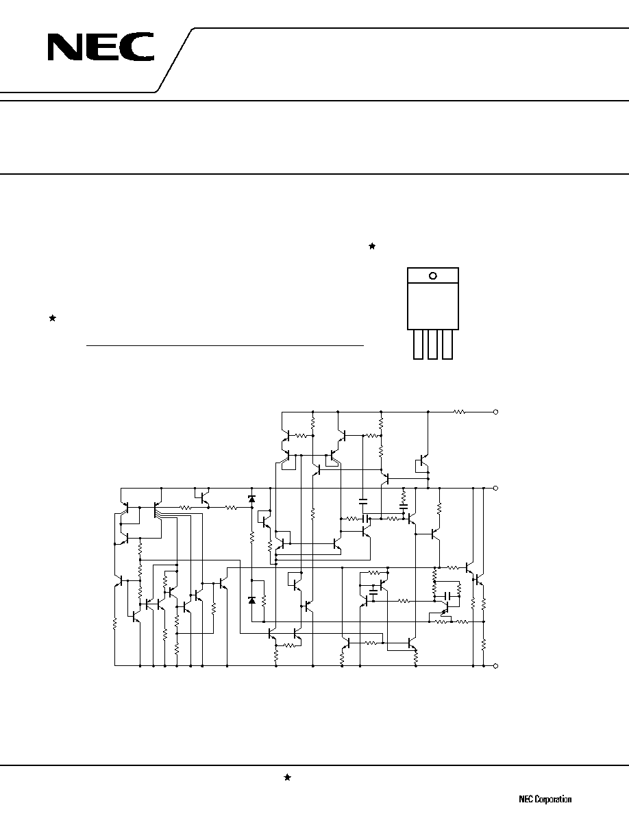
EQUIVALENT CIRCUIT
PIN CONFIGURATION (Marking Side)
The mark shows major revised points.
©
1986
DATA SHEET
1
2
3
1 : ADJ
2 : INPUT
3 : OUTPUT
Q
1
Q
2
R
41
R
36
R
2
R
3
R
8
R
5
R
37
R
39
R
28
R
29
R
40
R
34
R
33
R
35
R
11
R
10
R
38
R
27
R
32
R
31
R
30
R
26
R
25
R
7
R
6
R
9
R
24
R
23
R
22
R
13
R
14
R
16
R
17
R
15
R
18
R
20
R
19
R
21
C
3
C
1
C
2
C
4
C
5
R
4
R
1
R
42
Q
3
Q
4
Q
8
Q
5
Q
23
Q
7
Q
28
Q
6
D
2
D
3
D
6
D
5
D
4
D
1
Q
29
ADJ
OUTPUT
INPUT
Q
30
Q
25
Q
27
Q
26
Q
31
Q
24
Q
9
Q
13
Q
12
Q
14
Q
15
Q
16
Q
17
Q
18
Q
20
Q
21
Q
19
Q
22
Q
11
Q
10
D
7
2
µ
PC337
ABSOLUTE MAXIMUM RATINGS (T
A
= 25
∞
C, unless otherwise specified.)
Parameter
Symbol
Rating
Unit
Input-Output Voltage Differential
V
IN
≠ V
O
≠40
V
Total Power Dissipation
P
T
15
Note
V
Operating Ambient Temperature
T
A
≠20 to +85
∞
C
Operating Junction Temperature
T
J
≠20 to +150
∞
C
Storage Temperature
T
stg
≠65 to +150
∞
C
Thermal Resistance (junction to case)
R
th(J-C)
7
∞
C/W
Thermal Resistance (junction to ambient)
R
th(J-A)
65
∞
C/W
Note Internally limited.
When operating junction temperature rise up to 150
∞
C (
200
∞
C), the internal circuit shutdown output
voltage.
Caution Exposure to Absolute Maximum Ratings for extended periods may affect device reliability;
exceeding the ratings could cause permanent damage. The parameters apply independently.
The device should be operated within the limits specified under DC and AC Characteristics.
RECOMMENDED OPERATING CONDITIONS
Parameter
Symbol
MIN.
TYP.
MAX.
Unit
Input-Output Voltage Differential
V
IN
≠ V
O
≠3
≠5
≠38.7
V
Input Voltage
V
IN
≠4.3
≠40
V
Output Voltage
V
O
≠1.3
≠30
V
Output Current
I
O
0.01
1.5
A
Operating Junction Temperature
T
J
≠20
+125
∞
C
3
µ
PC337
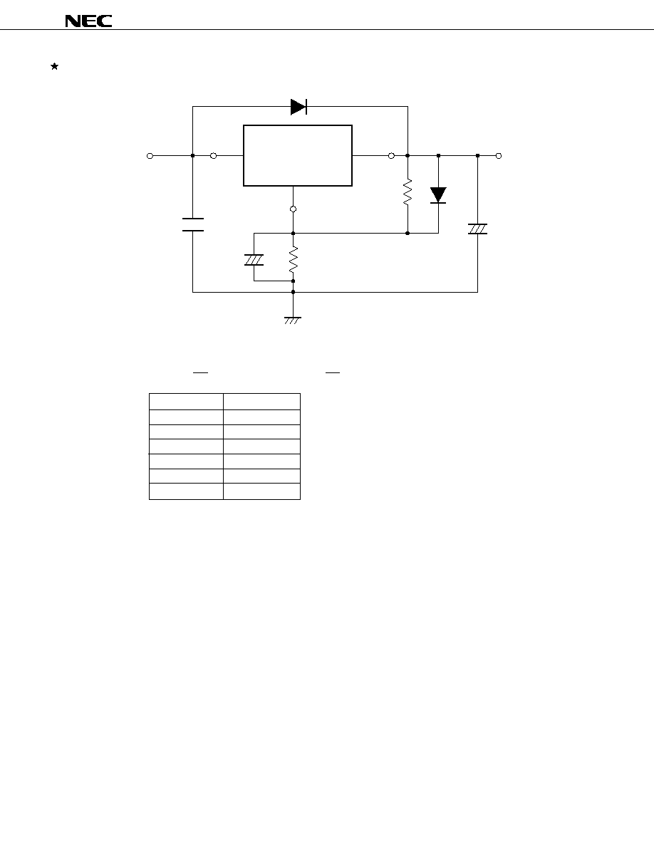
TYPICAL CONNECTION
Remark R
1
, R
2
: Resistor to set the output voltage.
V
O
= (1 + ) ∑ V
REF
+ I
ADJ
∑ R
2
= (1 + ) ∑ V
REF
V
O
(V)
R
2
(
: TYP.)
≠1.25
0
≠2.5
120
≠5.0
360
≠12
1032
≠24
2184
≠30
2760
C
IN
: Need to stop the oscillation for the long input wiring length.
C
O
: Need to stop the oscillation for the long output wiring length.
Improve the transient stability of the output voltage when the lord current is suddently changed.
C
ADJ
: Improve the ripple rejection and the oscillate rejection.
D
1
: Protect against C
ADJ
from output short.
D
2
: Need for V
IN
> V
O
.
R
2
R
1
R
2
R
1
∑
∑
PC337
INPUT
OUTPUT
C
ADJ
10 F
V
O
D
1
D
2
R
2
ADJ
R
1
120
C
IN
1 F
C
O
4.7 F
V
IN
+
+
µ
µ
µ
µ

4
µ
PC337
ELECTRICAL CHARACTERISTICS (V
IN
≠ V
O
= ≠5 V, I
O
= 0.5 A, 0
∞
C
T
J
+125
∞
C, unless otherwise
specified.)
Parameter
Symbol
Conditions
MIN.
TYP.
MAX.
Unit
Line Regulation
REG
IN
T
J
= 25
∞
C, 3 V
| V
IN
≠ V
O
|
40 V
Note
0.005
0.04
%/V
0
∞
C
T
J
125
∞
C, 3 V
| V
IN
≠ V
O
|
40 V
Note
0.01
0.07
%/V
Load Regulation
REG
L
T
J
= 25
∞
C,
| V
O
|
5 V
30
50
mV
10 mA
I
O
1.5 A
Note
| V
O
|
5 V
0.6
1.0
%
0
∞
C
T
J
125
∞
C,
| V
O
|
5 V
45
70
mV
10 mA
I
O
1.5 A
Note
| V
O
|
5 V
0.9
1.5
%
Thermal Regulation
REG
TH
T
J
= 25
∞
C, | V
IN
≠ V
O
| = 40 V, V
O
= ≠10 V,
0.005
0.04
%/W
0 A
I
O
0.25 A, t = 10 ms
ADJ pin Output Current
I
ADJ
60
100
µ
A
I
ADJ
Change
I
ADJ
T
J
= 25
∞
C, 3 V
| V
IN
≠ V
O
|
40 V,
2
5
µ
A
10 mA
I
O
1.5 A, P
T
15 W
Reference Voltage
V
REF
3 V
| V
IN
≠ V
O
|
40 V,
≠1.20
≠1.25
≠1.30
V
10 mA
I
O
1.5 A, P
T
15 W
Temperature Stability of
V
REF
/
T
0
∞
C
T
J
125
∞
C, I
O
= 5 mA
≠0.6
%
V
REF
Minimum Load Current
I
OMIN
.
| V
IN
≠ V
O
| = 40 V
2.1
10
mA
Peak Output Current
I
Opeak
3 V
| V
IN
≠ V
O
|
15 V
1.5
2.3
2.9
A
T
J
= 25
∞
C, | V
IN
≠ V
O
| = 40 V
0.15
0.8
A
Output Noise Voltage
V
n
T
J
= 25
∞
C, 10 H
Z
f
10 kHz
0.002
%
(RMS)
Ripple Rejection
R ∑ R
T
J
= 25
∞
C,
V
IN
= 1 V
r.m.s
C
ADJ
= 0
60
dB
f = 120 Hz, V
O
= ≠10 V
C
ADJ
= 10
µ
F
66
75
dB
Note Measured at constant junction temperature, using pulse testing with a low duty cycle.
PW = 10 ms, Duty Cycle
2 %
5
µ
PC337
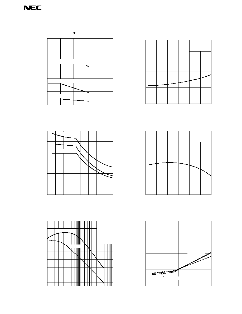
TYPICAL CHARACTERISTICS (T
A
= 25
∞
C, unless otherwise specified.)
REG
L
vs T
J
T
J
- Operating Junction Temperature -
∞
C
V
IN
= ≠10 V
V
O
= ≠5 V
REG
L
- Load Regulation -
%
V
REF
- Reference Voltage -
V
≠25
0
25
50
75
100
125
T
J
= ≠20
∞
C
+25
∞
C
+125
∞
C
V
IN
≠V
O
= ≠5 V
I
O
= 10 mA
C
ADJ
= 10 F
V
IN
= ≠15 V
V
O
= ≠10 V
I
O
= 0.5 A
C
IN
= 1 F
C
O
= 4.7 F
C
ADJ
= 0
T
J
= ≠20
∞
C
T
J
= +125
∞
C
T
J
= +25
∞
C
P
T
- Total Power Dissipation - W
I
Opeak
- Peak Output Current - A
R
. R
- Ripple Rejection - dB
I
OMIN.
- Minimum Load Current -
mA
T
A
- Operating Ambient Temperature -
∞
C
I
Opeak
vs V
DIF
V
REF
vs T
J
V
DIF
- Input - Output Voltage Differential - V
f - Frequency - Hz
V
DIF
- Input - Output Voltage Differential - V
R . R vs V
O
I
OMIN.
vs V
DIF
T
J
- Operating Junction Temperature -
∞
C
P
T
vs T
A
25
50
75
100
125
25
20
15
10
≠1.27
5
0
With 10
∞
C/W heatsink
No heatsink
Infinite heatsink
≠10
10
≠10
≠20
≠30
≠40
100
1 k
10 k
100 k
≠25
0
25
50
75
100
125
≠20
≠30
≠40
2.0
1.5
1.0
0.5
0
≠1.26
≠1.25
≠1.24
≠1.23
0
1.0
2.0
3.0
0
1
2
3
4
90
80
70
60
50
40
30
20
10
µ
µ
µ