The information in this document is subject to change without notice. Before using this document, please
confirm that this is the latest version.
Not all products and/or types are available in every country. Please check with an NEC Electronics
sales representative for availability and additional information.
JUNCTION FIELD EFFECT TRANSISTOR
2SK3653B
N-CHANNEL SILICON JUNCTION FIELD EFFECT TRANSISTOR
FOR IMPEDANCE CONVERTER OF ECM
DATA SHEET
Document No. D17284EJ1V0DS00 (1st edition)
Date Published August 2004 NS CP(K)
Printed in Japan
2004
DESCRIPTION
The 2SK3653B is suitable for converter of ECM.
General-purpose product.
FEATURES
∑ Low noise:
-108.5 dB TYP. (V
DD
= 2.0 V, C = 5 pF, R
L
= 2.2 k
)
∑ Especially suitable for audio and telephone
∑ Super thin thickness package:
t = 0.37 mm TYP.
ORDERING INFORMATION
PART NUMBER
PACKAGE
2SK3653B
3pXSOF (0814)
ABSOLUTE MAXIMUM RATINGS (T
A
= 25∞C)
Drain to Source Voltage (V
GS
=
-1.0 V)
V
DSX
20 V
Gate to Drain Voltage
V
GDO
-20 V
Drain Current
I
D
10
mA
Gate Current
I
G
10
mA
Total Power Dissipation
P
T
100
mW
Junction Temperature
T
j
125
∞C
Storage Temperature
T
stg
-55 to +125
∞C
Caution Please take care of ESD (Electro Static Discharge) when you handle the device in this document.
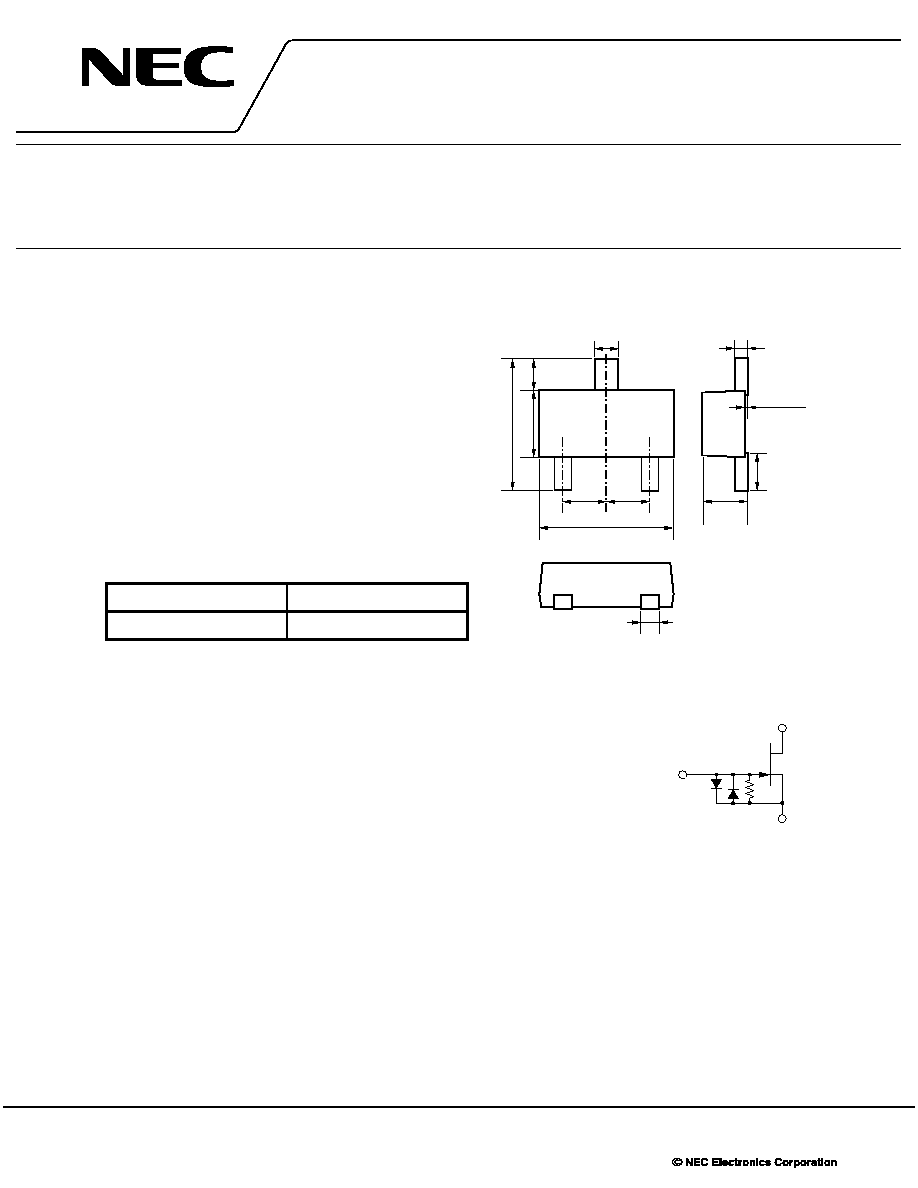
PACKAGE DRAWING (Unit: mm)
0.3 ±0.05
1.2 ±0.1
MAX. 0.4
0.8 ±0.1
1.4 ±0.1
0 to 0.05
0.13
+0.1
≠0.05
0.2
+0.1
≠0
0.2
2
0.45
0.45
3
1
(0.26)
EQUIVALENT CIRCUIT
3
2
1
1: Source
2: Drain
3: Gate
Data Sheet D17284EJ1V0DS
2
2SK3653B
ELECTRICAL CHARACTERISTICS (T
A
= 25∞C)
CHARACTERISTICS SYMBOL
TEST
CONDITIONS
MIN.
TYP.
MAX.
UNIT
Zero Gate Voltage Drain Cut-off Current
I
DSS
V
DS
= 2.0 V, V
GS
= 0 V
90
200
430
µ
A
Gate Cut-off Voltage
V
GS(off)
V
DS
= 2.0
V, I
D
= 1.0
µ
A
-0.37
-1.0 V
Forward Transfer Admittance
| y
fs1
| V
DS
= 2.0 V, I
D
= 30
µ
A, f = 1.0 kHz
300
480
µ
S
| y
fs2
| V
DS
= 2.0 V, V
GS
= 0 V, f = 1.0 kHz
750
1300
µ
S
Input Capacitance
C
iss
V
DS
= 2.0 V, V
GS
= 0 V, f = 1.0 MHz
4.0
pF
Voltage Gain
G
V
V
DD
= 2.0 V, C = 5 pF, R
L
= 2.2 k
, -1.0 dB
V
IN
= 10 mV, f = 1 kHz
Noise Voltage
NV V
DD
= 2.0 V, C = 5 pF, R
L
= 2.2 k
, -108.5 dB
A-curve
I
DSS
CLASSIFICATION
MARKING CE
CF
CH
CJ
I
DSS
(
µ
A)
90 to 180
150 to 240
210 to 350
320 to 430
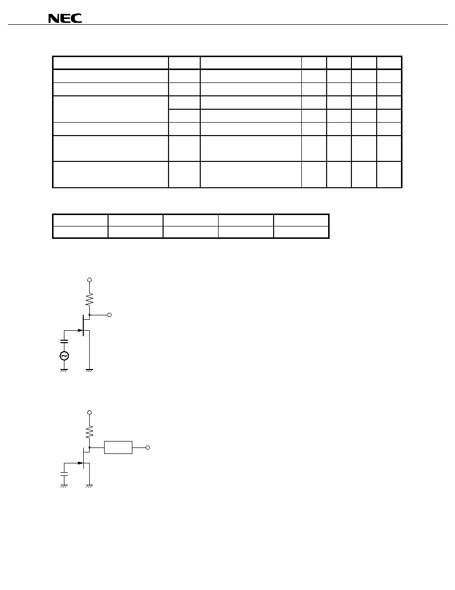
VOLTAGE GAIN TEST CIRCUIT
C
R
L
V
DD
Out
NOISE VOLTAGE TEST CIRCUIT
C
R
L
V
DD
NV (r.m.s)
JIS A
Data Sheet D17284EJ1V0DS
3
2SK3653B
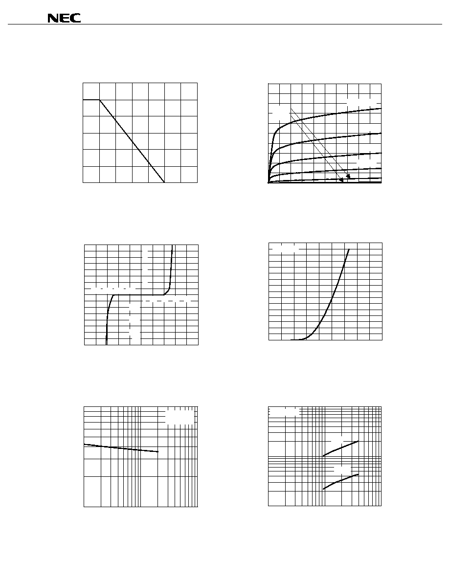
TYPICAL CHARACTERISTICS (T
A
= 25∞C)
DERATING FACTOR OF POWER DISSIPATION
DRAIN CURRENT vs.
DRAIN TO SOURCE VOLTAGE
dT - D
e
rating F
a
ctor - %
0
20
40
60
80
100
120
0
25
50
75
100
125
150
175
T
A
- Ambient Temperature - ∞C
I
D
- Dr
ain Cur
r
ent
-
µ
A
0
200
400
600
800
1000
0
2
4
6
8
10
0 V
-0.2 V
-0.3 V
-0.1 V
V
GS
= 0.2 V
0.1 V
V
DS
- Drain to Source Voltage - V
GATE TO SOURCE CURRENT vs.
GATE TO SOURCE VOLTAGE
DRAIN CURRENT vs.
GATE TO SOURCE VOLTAGE
I
GS
-
Gate to So
u
r
ce Current -
µ
A
0
10
20
30
40
-10
-20
-30
-40
0.2 0.4 0.6 0.8
-0.2
-0.4
-0.6
-0.8
V
GS
- Gate to Source Voltage - V
I
D
- Dr
ain Cur
r
ent
-
µ
A
0
200
400
600
800
1000
1200
1400
1600
-0.8 -0.6 -0.4 -0.2
0
0.2 0.4 0.6 0.8
1
V
DS
= 2.0 V
V
GS
- Gate to Source Voltage - V
INPUT CAPACITANCE vs.
DRAIN TO SOURCE VOLTAGE
FORWARD TRANSFER ADMITTANCE AND GATE
CUT-OFF VOLTAGE vs. ZERO GATE VOLTAGE
DRAIN CURRENT
C
is
s
- Input C
apa
citance - pF
1
10
1
10
100
V
GS
= 0 V
f = 1.0 MHz
V
DS
- Drain to Source Voltage - V
| y
fs
| - Forward
T
r
ansfer Admittan
c
e - mS
V
G
S
(off)
-
Gate C
u
t
-
off Voltage - V
0.1
1
10
10
100
1000
| y
fs
|
V
GS(off)
V
DS
= 2.0 V
I
DSS
- Zero Gate Voltage Drain Current -
µ
A
2SK3653B
The information in this document is current as of August, 2004. The information is subject to
change without notice. For actual design-in, refer to the latest publications of NEC Electronics data
sheets or data books, etc., for the most up-to-date specifications of NEC Electronics products. Not
all products and/or types are available in every country. Please check with an NEC Electronics sales
representative for availability and additional information.
No part of this document may be copied or reproduced in any form or by any means without the prior
written consent of NEC Electronics. NEC Electronics assumes no responsibility for any errors that may
appear in this document.
NEC Electronics does not assume any liability for infringement of patents, copyrights or other intellectual
property rights of third parties by or arising from the use of NEC Electronics products listed in this document
or any other liability arising from the use of such products. No license, express, implied or otherwise, is
granted under any patents, copyrights or other intellectual property rights of NEC Electronics or others.
Descriptions of circuits, software and other related information in this document are provided for illustrative
purposes in semiconductor product operation and application examples. The incorporation of these
circuits, software and information in the design of a customer's equipment shall be done under the full
responsibility of the customer. NEC Electronics assumes no responsibility for any losses incurred by
customers or third parties arising from the use of these circuits, software and information.
While NEC Electronics endeavors to enhance the quality, reliability and safety of NEC Electronics products,
customers agree and acknowledge that the possibility of defects thereof cannot be eliminated entirely. To
minimize risks of damage to property or injury (including death) to persons arising from defects in NEC
Electronics products, customers must incorporate sufficient safety measures in their design, such as
redundancy, fire-containment and anti-failure features.
NEC Electronics products are classified into the following three quality grades: "Standard", "Special" and
"Specific".
The "Specific" quality grade applies only to NEC Electronics products developed based on a customer-
designated "quality assurance program" for a specific application. The recommended applications of an NEC
Electronics product depend on its quality grade, as indicated below. Customers must check the quality grade of
each NEC Electronics product before using it in a particular application.
"Standard": Computers, office equipment, communications equipment, test and measurement equipment, audio
and visual equipment, home electronic appliances, machine tools, personal electronic equipment
and industrial robots.
"Special":
Transportation equipment (automobiles, trains, ships, etc.), traffic control systems, anti-disaster
systems, anti-crime systems, safety equipment and medical equipment (not specifically designed
for life support).
"Specific": Aircraft, aerospace equipment, submersible repeaters, nuclear reactor control systems, life
support systems and medical equipment for life support, etc.
The quality grade of NEC Electronics products is "Standard" unless otherwise expressly specified in NEC
Electronics data sheets or data books, etc. If customers wish to use NEC Electronics products in applications
not intended by NEC Electronics, they must contact an NEC Electronics sales representative in advance to
determine NEC Electronics' willingness to support a given application.
(Note)
(1) "NEC Electronics" as used in this statement means NEC Electronics Corporation and also includes its
majority-owned subsidiaries.
(2) "NEC Electronics products" means any product developed or manufactured by or for NEC Electronics (as
defined above).
∑
∑
∑
∑
∑
∑
M8E 02. 11-1