 | –≠–ª–µ–∫—Ç—Ä–æ–Ω–Ω—ã–π –∫–æ–º–ø–æ–Ω–µ–Ω—Ç: 3SK177 | –°–∫–∞—á–∞—Ç—å:  PDF PDF  ZIP ZIP |
©
1995
DATA SHEET
MES FIELD EFFECT TRANSISTOR
Document No. P10412EJ1V0DS00 (1st edition)
(Previous No. TN-1877)
Date Published August 1995 P
Printed in Japan
3SK177
FEATURES
∑
Suitable for use as RF amplifier in UHF TV tuner.
∑
Low C
rss
: 0.02 pF TYP.
∑
High G
PS
: 20 dB TYP.
∑
Low NF : 1.1 dB TYP.
ABSOLUTE MAXIMUM RATINGS (T
A
= 25 ∞C)
Drain to Source Voltage
V
DSX
13
V
Gate 1 to Source Voltage
V
G1S
≠4.5
V
Gate2 to Source Voltage
V
G2S
≠4.5
V
Drain Current
I
D
40
mA
Total Power Dissipation
P
T
200
mW
Channel Temperature
T
ch
125
∞C
Storage Temperature
T
stg
≠55 to +125
∞C
ELECTRICAL CHARACTERISTICS (T
A
= 25 ∞C)
CHARACTERISTIC
SYMBOL
MIN.
TYP.
MAX.
UNIT
TEST CONDITIONS
Drain to Source Breakdown Voltage
BV
DSX
13
V
V
G1S
= ≠4 V, V
G2S
= 0, I
D
= 10
µ
A
Drain Current
I
DSS
5
20
40
mA
V
DS
= 5 V, V
G2S
= 0, V
G1S
= 0
Gate1 to Source Cutoff Voltage
V
G1S(off)
≠3.5
V
V
DS
= 5 V, V
G2S
= 0, I
D
= 100
µ
A
Gate2 TO Source Cutoff Voltage
V
G2S(off)
≠3.5
V
V
DS
= 5 V, V
G1S
= 0, I
D
= 100
µ
A
Gate1 Reverse Current
I
G1SS
10
µ
A
V
DS
= 0, V
G1S
= ≠4 V, V
G2S
= 0
Gate2 Reverse Current
I
G2SS
10
µ
A
V
DS
= 0, V
G2S
= ≠4 V, V
G1S
= 0
Forward Transter Admittance
| y
fs
|
18
25
35
ms
V
DS
= 5 V, V
G2S
= 1 V, I
D
= 10 mA,
f = 1.0 kHz
Input Capacitance
C
iss
0.5
1.0
1.5
pF
V
DS
= 5 V, V
G2S
= 1 V, I
D
= 10 mA,
Reverse Transfer Capacitance
C
rss
0.02
0.03
pF
f = 1 MHz
Power Gain
G
PS
16.0
20.0
dB
V
DS
= 5 V, V
G2S
= 1 V, I
D
= 10 mA,
Noise Figure
NF
1.1
2.5
dB
f = 900 MHz
I
DSS
Classification
Unit: mA
Class
U71
U72
U73
U74
Marking
U71
U72
U73
U74
I
DSS
5 to 15
10 to 25
20 to 35
30 to 40
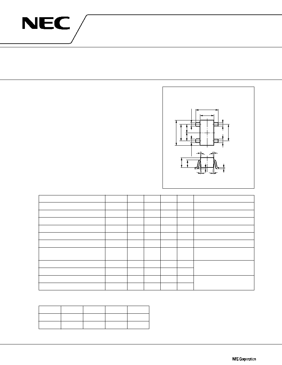
RF AMP. FOR UHF TV TUNER
N-CHANNEL GaAs DUAL-GATE MES FIELD-EFFECT TRANSISTOR
4 PIN MINI MOLD
2.8
≠0.3
+0.2
1.5
≠0.1
+0.2
0.4
≠0.05
+0.1
29.02
(1.8)
0.85
0.95
2
1
3
4
0.4
≠0.05
+0.1
(1.9)
0.16
≠0.06
+0.1
0.4
≠0.05
+0.1
1.1
≠0.1
+0.2
0.6
≠0.05
+0.1
0.8
0 to 0.1
5∞
5∞
5∞
5∞
1. Source
2. Drain
3. Gate 2
4. Gate 1
PACKAGE DIMENSIONS
in millimeters
3SK177
2
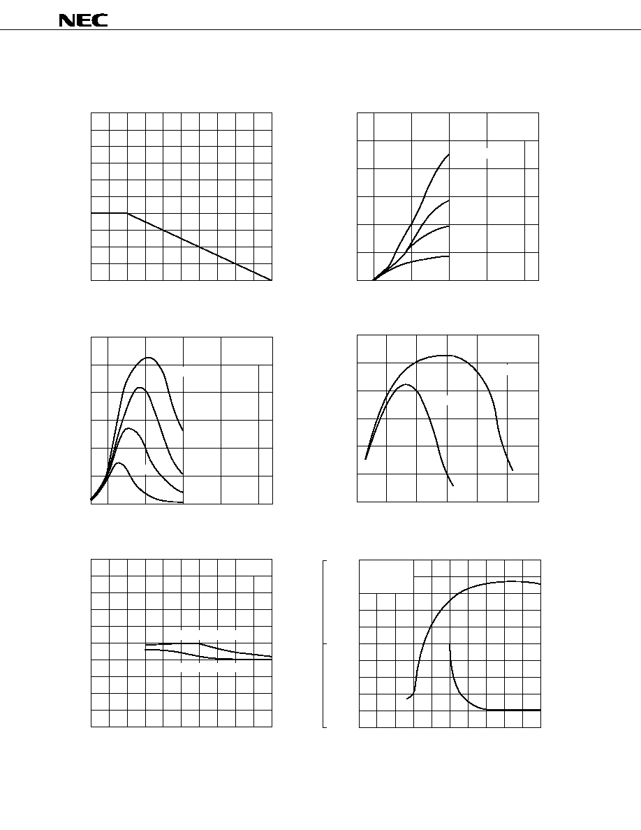
TYPICAL CHARACTERISTICS (T
A
= 25 ∞C)
30
20
10
0
≠1.0
0
+1.0
DRAIN CURRENT vs.
GATE1 TO SOURCE VOLTAGE
V
G2S
= 1.0 V
0.5 V
0 V
≠0.5 V
V
DS
= 5 V
V
G1S
≠ Gate 1 to Source Voltage ≠ V
I
D
≠ Drain Current ≠ mA
FORWARD TRANSFER ADMITTANCE vs.
DRAIN CURRENT
V
DS
= 5 V
f = 1 kHz
V
G2S
= 1.0 V
V
G2S
= 0.5 V
0
10
20
30
I
D
≠ Drain Current ≠ mA
30
20
10
y
fs
≠ Forward Transfer Admittance ≠ mS
FOWER GAIN AND NOISE FIGURE vs.
GATE2 TO SOURCE VOLTAGE
V
DS
= 5 V
V
G2S
= 1 V
at I
D
= 10 mA
f = 900 MHz
≠3.0
≠2.0
+1.0
+2.0
V
G2S
≠ Gate 2 to Source Voltage ≠ V
30
15
≠30
≠45
G
PS
≠ Power Gain ≠ dB
0
≠15
≠1.0
0
G
PS
NF
NF ≠ Noise Figure ≠ dB
10
5
0
300
100
0
75
125
TOTAL POWER DISSIPATION vs.
AMBIENT TEMPERATURE
T
A
≠ Ambient Temperature ≠ ∞C
P
T
≠ Total Power Dissipation ≠ mW
100
50
25
200
400
30
20
10
0
≠1.0
0
+1.0
FORWARD TRANSFER ADMITTANCE vs.
GATE1 TO SOURCE VOLTAGE
V
G2S
= 1.0 V
0.5 V
0 V
V
DS
= 5 V
f = 1 kHz
V
G1S
≠ Gate 1 to Source Voltage ≠ V
y
fs
≠ Forward Transfer Admittance ≠ mS
≠0.5 V
2.0
1.0
0
0
+1.0
INPUT CAPACITANCE vs.
GATE2 TO SOURCE VOLTAGE
V
DS
= 5 V
f = 1 MHz
V
G2S
≠ Gate 2 to Source Voltage ≠ V
C
iss
≠ Input Capacitance ≠ pF
≠1.0
V
G2S
= 1 V at I
D
= 5 mA
V
G2S
= 1 V at I
D
= 10 mA

3SK177
3
POWER GAIN AND NOISE FIGURE vs.
DRAIN CURRENT
V
DS
= 5 V
V
G2S
= 1 V
f = 900 MHz
10
I
D
≠ Drain Current ≠ mA
25
20
5
0
G
PS
≠ Power Gain ≠ dB
15
10
5
NF
NF ≠ Noise Figure ≠ dB
10
5
0
G
PS
POWER GAIN AND NOISE FIGURE vs.
DRAIN TO SOURCE VOLTAGE
10
V
DS
≠ Drain to Source Voltage ≠ V
20
0
G
PS
≠ Power Gain ≠ dB
10
5
NF
NF ≠ Noise Figure ≠ dB
10
5
0
V
G2S
= 1 V
V
G2S
= 0.5 V
V
G2S
= 2 V
I
D
= 10 mA
f = 900 MHz
G
PS
S-PARAMETER (V
DS
= 5 V, V
G2S
= 1 V, I
D
= 10 mA)
FREQUENCY
S11
S21
S12
S22
MHz
MAG
ANG
MAG
ANG
MAG
ANG
MAG
ANG
100.0000
0.999
≠3.3
2.359
177.2
0.006
≠122.3
0.969
≠1.3
200.0000
1.000
≠7.2
2.389
169.3
0.004
123.0
0.981
≠2.9
300.0000
0.998
≠9.3
2.313
164.4
0.000
≠145.0
0.979
≠3.3
400.0000
0.974
≠13.4
2.233
160.0
0.004
79.2
0.967
≠5.6
500.0000
1.005
≠15.7
2.420
l58.4
0.007
29.7
0.999
≠5.8
600.0000
0.942
≠19.1
2.300
150.0
0.003
65.0
0.958
≠7.7
700.0000
0.968
≠22.2
2.332
145.5
0.004
45.5
0.997
≠8.5
800.0000
0.920
≠25.2
2.229
141.5
0.008
80.1
0.957
≠9.4
900.0000
0.952
≠28.9
2.447
136.8
0.004
8.3
0.999
≠12.5
1000.0000
0.898
≠29.4
2.303
131.1
0.001
50.9
0.968
≠11.1
1100.0000
0.915
≠35.1
2.348
125.8
0.004
71.4
0.984
≠14.8
1200.0000
0.879
≠35.2
2.367
123.5
0.000
91.1
0.989
≠13.0
3SK177
4
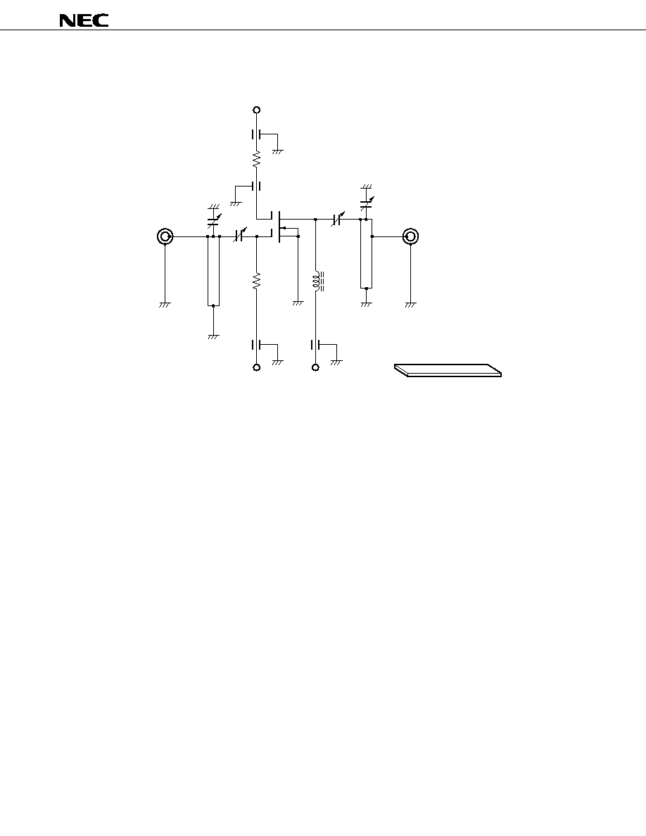
900 MHz G
PS
AND NF TEST CIRCUIT
V
G2S
(1 V)
1 000 pF
47 k
1 000 pF
to 10 pF
OUTPUT
50
to 10 pF
INPUT
50
to 10 pF
to 10 pF
1 000 pF
1 000 pF
L
2
L
1
47 k
RFC
V
G1S
V
DD
(5 V)
L
1
, L
2
, 35
◊
5
◊
0.2 mm
V
DS
= 5 V, V
G2S
= 1 V, I
D
= 10 mA

3SK177
5
[MEMO]

2
3SK177
No part of this document may be copied or reproduced in any form or by any means without the prior written
consent of NEC Corporation. NEC Corporation assumes no responsibility for any errors which may appear in this
document.
NEC Corporation does not assume any liability for infringement of patents, copyrights or other intellectual
property rights of third parties by or arising from use of a device described herein or any other liability arising
from use of such device. No license, either express, implied or otherwise, is granted under any patents,
copyrights or other intellectual property rights of NEC Corporation or others.
While NEC Corporation has been making continuous effort to enhance the reliability of its semiconductor devices,
the possibility of defects cannot be eliminated entirely. To minimize risks of damage or injury to persons or
property arising from a defect in an NEC semiconductor device, customer must incorporate sufficient safety
measures in its design, such as redundancy, fire-containment, and anti-failure features.
NEC devices are classified into the following three quality grades:
"Standard", "Special", and "Specific". The Specific quality grade applies only to devices developed based on
a customer designated "quality assurance program" for a specific application. The recommended applications
of a device depend on its quality grade, as indicated below. Customers must check the quality grade of each
device before using it in a particular application.
Standard: Computers, office equipment, communications equipment, test and measurement equipment,
audio and visual equipment, home electronic appliances, machine tools, personal electronic
equipment and industrial robots
Special:
Transportation equipment (automobiles, trains, ships, etc.), traffic control systems, anti-disaster
systems, anti-crime systems, safety equipment and medical equipment (not specifically designed
for life support)
Specific: Aircrafts, aerospace equipment, submersible repeaters, nuclear reactor control systems, life
support systems or medical equipment for life support, etc.
The quality grade of NEC devices in "Standard" unless otherwise specified in NEC's Data Sheets or Data Books.
If customers intend to use NEC devices for applications other than those specified for Standard quality grade,
they should contact NEC Sales Representative in advance.
Anti-radioactive design is not implemented in this product.
M4 94.11