BIPOLAR ANALOG INTEGRATED CIRCUIT
µ
PC1851B
I
2
C BUS-COMPATIBLE US MTS PROCESSING LSI
The
µ
PC1851B is an integrated circuit for US MTS (Multiplexed Television Sound) system with the addition of
the I
2
C bus interface. All functions required for US MTS system are incorporated on a single chip.
The
µ
PC1851B allows users to switch modes, control volume and tone, and adjust the separation circuit
through the I
2
C bus.
FEATURES
∑ Stereo demodulation, SAP (Sub Audio Program) demodulation, dbx noise reduction decoding, I
2
C bus interface,
input selector (2 channels), surround processor (1 phase), volume and tone control circuits incorporated on a single
chip
∑ Mode switching, volume and tone control, and separation adjustment through the I
2
C bus
∑ Power supply: 8 V to 10 V
∑ On-chip input attenuator for simple interface with intermediate frequency processing IC (I
2
C bus control)
∑ Output level: 1.4 V
p-p
(with L+R signals, 100 % modulation)
APPLICATION
∑ TV sets and VCRs for north America
ORDERING INFORMATION
Part Number
Package
µ
PC1851BCU
42-pin plastic SDIP (15.24 mm (600))
The
µ
PC1851B is available only to licensees of THAT Corporation.
For information, please call: (508) 229-2500 (U.S.A), or (03) 5790-5391 (Tokyo).
The information in this document is subject to change without notice. Before using this document, please
confirm that this is the latest version.
Not all devices/types available in every country. Please check with local NEC representative for availability
and additional information.
The mark shows major revised points.
©
1998
DATA SHEET
Document No. S13417EJ2V0DS00 (2nd edition)
Date Published June 2000 N CP(K)
Printed in Japan
3
µ
PC1851B
Data Sheet S13417EJ2V0DS00
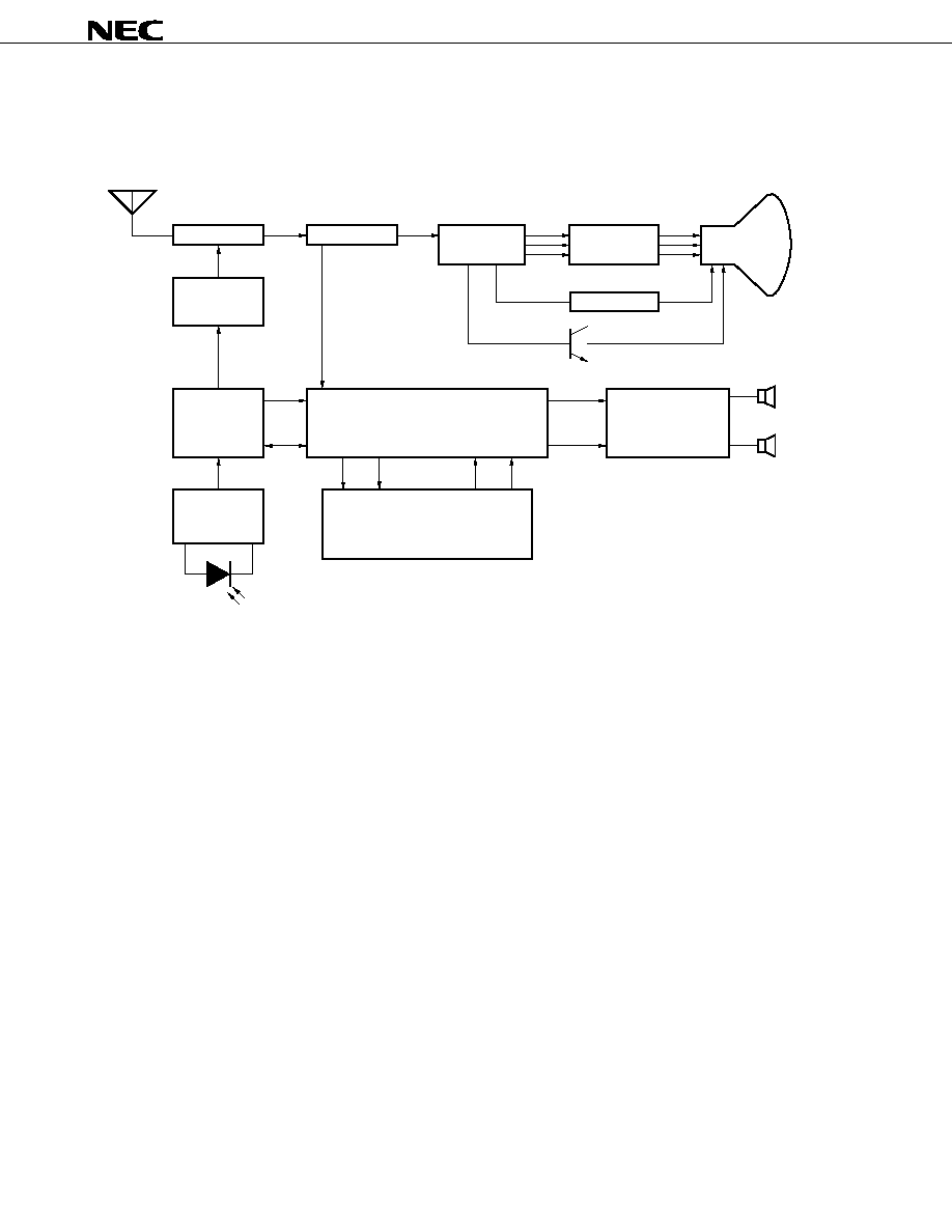
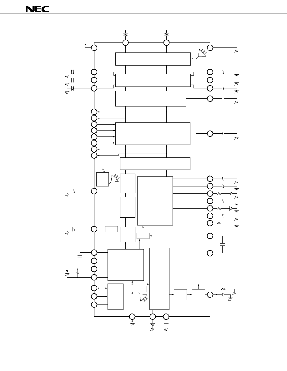
BLOCK DIAGRAM
DGND 24
SCL
23
SDA 22
D2
6
D1
5
PD1
3
PD2
4
I
2
C Bus
Interface
L+R
LPF
Switch
1 F
0.1 F
2
1/2V
CC
+
22 F
VRE
42
+
1 F
MOA
MOR 34
35
38
36
39
37
41
40
MOL
ER1
ER2
EL1
EL2
FOL
FOR
Input Attenuator
7
D/A
Filter
Control
Filter
32
31
33
+
0.1 F
LBC
+
2.2 F
TLO
2200 pF
LTC
1
V
CC
26
LOT
+
10 F
25
ROT
+
10 F
29
28
30
21
+
RBC
TRO
RTC
+
AGND
0.1 F
2200 pF
2.2 F
0.022 F
27
SUR
0.1 F
Noise
BPF
Noise
Detector
D/A
9
COM
+
2.2 F
12
+
8
SOA
0.1 F
SDT
0.047 F
15
18
14
13
17
16
20
11
10
VOA
WTI**
WRB
STI**
SRB
dO
ITI*
SI
SOT
++
+
3.3 F
5.1 k
+
10 F
16.6 k
0.47 F
68 k
1 k
4.7 F
I
2
C Bus
Interface
+
1 F
+
+
3 k
+
NDT
1 F
1 F
1 F
19
VOL-C
+
4.7 F
D/A
Volume Control
Tone Control
Surround Block
Matrix Block
Selector Block
dbx Noise
Reduction Block
Offset
Absorption
De-
emphasis
SAP
Demodulation
Block
Stereo
Demodulation
Block
9 V
+
µ
µ
µ
µ
µ
µ
µ
µ
µ
µ
µ
µ
µ
µ
µ
µ
µ
µ
µ
µ
µ
µ
µ
µ
Remark Use the followings for external parts.
Resistor (*): Metal film resistor (
±
1 %). Unless otherwise specified;
±
5 %
Capacitors (**): Tantalum capacitor (
±
10 %). Unless otherwise specified;
±
20 %
5
µ
PC1851B
Data Sheet S13417EJ2V0DS00
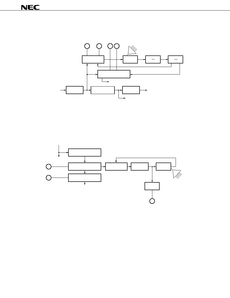
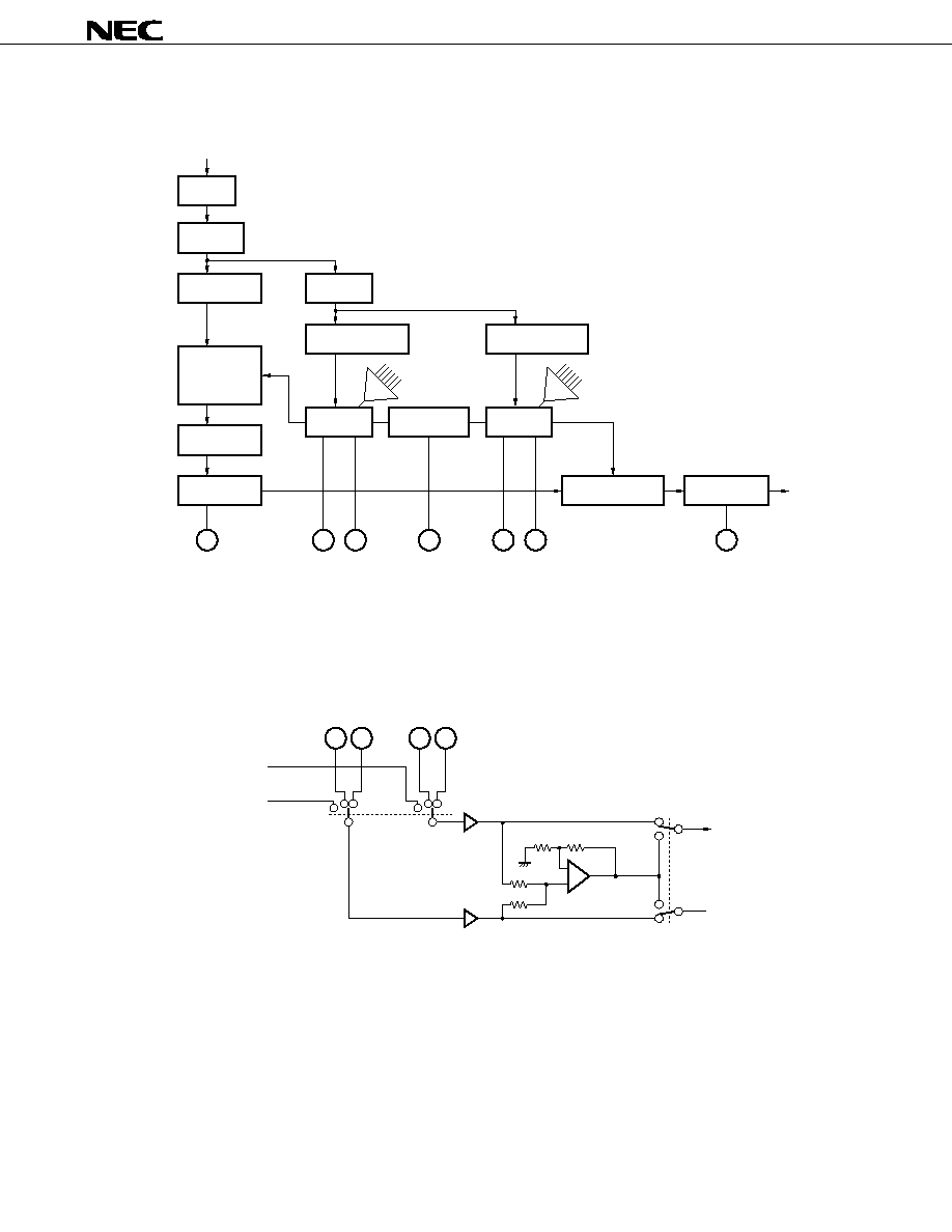
dbx NOISE REDUCTION BLOCK
SELECTOR BLOCK
Notes 1. Switch (TV signal/External input 1/External input 2).
2. The input gain 0 dB/6 dB can be selected by the command of the I
2
C bus (refer to 4.3 (5) Input gain).
From Switch
LPF
f
H
Trap
408-Hz LPF
2 f
H
Trap
2.19-kHz LPF
Offset
Absorption
Spectral RMS Filter
Wide-band RMS
Filter
Wide-band VCA
Offset
Absorption
To Matrix Block
18
dO
14
SRB
13
STI
16
WTI
17
WRB
20
VOA
D/A
D/A
Spectral
RMS
Timing Current
15
ITI
Variable
Emphasis
Wide-band
RMS
40 k
38
ER1
36
ER2
39
EL1
37
EL2
40 k
≠
+
40 k
40 k
To Surround Block
To Surround Block
Switch (Monaural/Stereo)
Switch
Note1
From Matrix Block
(L-channel signal)
From Matrix Block
(R-channel signal)
Note2
Note2