 | –≠–ª–µ–∫—Ç—Ä–æ–Ω–Ω—ã–π –∫–æ–º–ø–æ–Ω–µ–Ω—Ç: CMOS-8LCX | –°–∫–∞—á–∞—Ç—å:  PDF PDF  ZIP ZIP |
Document Outline
- Description
- Features
- Circuit Architecture
- Output Slew-Rate Selection
- Publications
- Absolute Maximum Ratings
- NECês ASIC Design System
- CrossCheck Test Design Flow
- CrossCheck Test Benefits
- Designing with CrossCheck
- Embedded Test Structures
- Test Controller
- Fault Models
- Automatic Test Pattern Generation
- Block Library List
NEC Electronics Inc.
Table 1 Gate Array Sizes
Device
Metal
Available
Usable
Total
µPD658xx
Layers
Gates
Gates
Pads
23
3
39,856
31,884
284
25
3
50,880
40,704
316
26
3
60,320
48,256
340
28
3
80,400
64,320
388
30
3
103,360
82,688
436
31
3
153,264
122,611
524
32
3
200,128
160,102
596
33
3
255,360
204,288
688
35
3
347,200
277,760
772
38
3
486,048
388,838
908
October 1993
Description
NEC's 3-volt CMOS-8LCX family consists of ultra-high
performance, sub-micron gate arrays, targeted for
applications requiring extensive integration and high
speeds. The device processing includes a true 3-volt,
0.5-micron (drawn) silicon-gate CMOS technology and
three-layer metalization. This technology features
channelless (sea-of-gates) architecture with an internal
gate delay of 131 ps (F/O = 1; L = 0 mm).
The µPD658xx series of 3-volt CrossCheck
Æ
-supported
devices consists of 10 masters, offered in densities of
10K gates to 486K gates. Usable gates range from 32K
gates to 389K gates. These gate arrays are ideal for use
in engineering workstations, high-end PCs, mainframes
and LAN products, where extensive integration and high
speed are primary design goals. CMOS-8LCX gate
arrays are also well-suited for all battery-operated
applications where high performance and low power
consumption are critical; and feasible only with a truly
optimized 3-volt CMOS process.
Features
®
Supports CrossCheck on-chip testability circuitry
®
Internal gate delays of 131 ps (F/O = 1; L = 0 mm)
®
Channelless, 0.50 µm CMOS architecture
®
Power (typ.) = 1.24 (3.3V) = 0.80 (3.0V)
®
Process technology designed for 3V operation
®
I/Os interface directly to 5V logic
®
48mA GTL I/O buffers are in development
®
Phase Locked Loop (PLL) for chip-to-chip clock
synchronization in development
®
Automated generation of clock network for skew
minimization
®
High pad to gate ratio optimizes silicon usage
®
Fully configurable high-speed RAM compiler
®
Advanced package options include TAB/QFP, TQFP,
PQFP, PGA and TAB
®
Libraries characterized at 3V±10% and 3.3V±0.3V
®
Variable output drive: 3, 6, 9, 12, 18, 24 or 48 mA
®
Slew-rate controlled output buffers
®
Supports scan test methodology
®
Single/Dual-Port RAM and ROM memory blocks
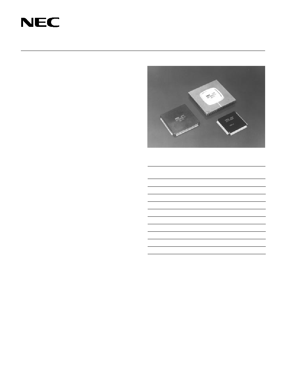
Figure 1. Various CMOS-8LCX Packages
70147-2
CMOS-8LCX
3-VOLT, 0.50-MICRON
CMOS GATE ARRAYS
CROSSCHECK TEST SUPPORT
Actual gate utilitization may vary depending on circuit implementation.
Utilization is 70% for three-layer metal.
Depending on package and circuit specification, some pads are used
for V
DD
and GND and are not available as signal pads.
Preliminary
Æ OpenCAD is a registered trademark of NEC Electronics Inc.
Æ CrossCheck is a registered trademark of CrossCheck Technology, Inc.
CMOS-8LCX products are fully supported by NEC's ad-
vanced ASIC design technology. NEC's OpenCAD
Æ
inte-
gration system lets the designer choose the most powerful
design tools and services available.
CMOS-8LCX gate arrays support automatic test genera-
tion through CrossCheck Technology's testability struc-
tures. This results in high fault coverage ATPT of synchro-
nous and asynchronous designs with no netlist modifica-
tions and without designer involvement.
CMOS-8LCX
2
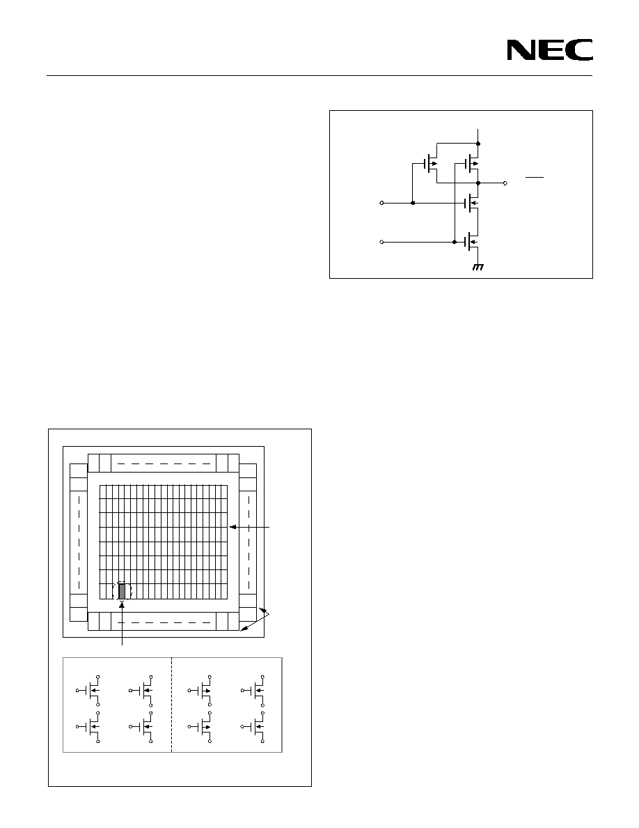
Figure 3. Cell Configured as a Two-Input NAND
Circuit Architecture
CMOS-8LCX products are built with NEC's 0.50-micron
(drawn) channelless gate array architecture. As shown
in figure 2, CMOS gate array chips are divided into I/O
and internal cell areas. The I/O cell area contains input
and output buffers that isolate the internal cells from
high-energy external signals. The internal cell area is an
array of basic cells, each composed of two p-channel
MOS transistors and two n-channel MOS transistors, as
well as four additional n-channel MOS transistors for
compact RAM design. A cell configured as a two-input
NAND gate is shown in figure 3. These p-channel and
n-channel transistors are sized to offer a superb ratio of
speed to silicon area.
Output Slew-Rate Selection
Fast rise and fall times of CMOS output buffers can
cause system noise and signal overshoot. When an
unterminated line is being driven by a buffer, the
maximum line length is determined by the rise and fall
time of the output buffers and the round-trip signal delay
of the line.
As a general rule, the round-trip delay of the line should
not exceed the rise or fall time of the driving signal.
Transmission lines that are longer than those deter-
mined by this rule can degrade system performance due
to reflections and ringing. One benefit of slew-rate
output buffers is that longer interconnections on a PC
board and routing flexibility are possible.
ASIC designers, therefore, can slow down the output
edge-rate by using a slew-rate output buffer and thus
accommodate longer transmission lines on PC boards.
Slew-rate buffers also inject less noise into the internal
power and ground busses of the device, than their non-
slew-rate counterparts. As a consequence, slew-rate
buffers require fewer power/ground pairs for simul-
taneous switching outputs.
Publications
This data sheet contains preliminary specifications,
package information, and operational data for the
CMOS-8LCX gate array families. Additional design
information will be available in NEC's CMOS-8LCX
Block Library and CMOS-8LCX Design Manual. Contact
your local NEC Design Center or the NEC Literature
Center for further ASIC design information; see the back
of this data sheet for locations and phone numbers.
Figure 2. Chip Layout and Internal Cell
Configuration
O = A ∑ B
V
DD
A
B
Internal
Cell Area
I/O Cell
Area
Basic Cell
83DC-6225A
N-Channel
N-Channel
N-Channel
P-Channel
RAM
Logic
3
CMOS-8LCX
Recommended Operating Conditions
at
V
DD
= 3.3V ± 0.3V
Parameter
Symbol
Min
Max
Unit
Power supply voltage
V
DD
2.7
3.6
V
Ambient temperature
T
A
≠40
+85
∞C
Low-level input voltage, 3V
V
IL
0
0.3 V
DD
V
High-level input voltage, 3V
V
IH
0.7 V
DD
V
DD
V
Low-level input voltage, 5V
V
IL
0
0.8
V
High-level input voltage, 5V
V
IH
2.2
V
PP
V
Input rise or fall time
t
R
, t
F
0
200
ns
Input rise or fall time, Schmitt
t
R
, t
F
0
10
ms
Positive Schmitt-trigger voltage
V
P
TBD
TBD
V
Negative Schmitt-trigger voltage
V
N
TBD
TBD
V
Hysteresis voltage
V
H
TBD
TBD
V
Input/Output Capacitance
V
DD
= V
I
= 0 V; f = 1 MHz
Terminal
Symbol
Typ
Max
Unit
Input
C
IN
10
20
pF
Output
C
OUT
10
20
pF
I/O
C
I/O
10
20
pF
Note: (1) Values include package pin capacitance.
Absolute Maximum Ratings
Power supply voltage, V
DD
≠0.5 to +4.6 V
3V interface I/O voltage, V
I
, V
O
≠0.5 V to V
DD
+ 0.5 V
5V interface I/O voltage, V
I
, V
O
≠0.5 V to V
DD
+ 3.0 V
Latch-up current, I
LATCH
>1 A (typ)
Operating temperature, T
OPT
≠40 to +85∞C
Storage temperature, T
STG
≠65 to +150∞C
Caution: Exposure to absolute maximum ratings for extended
periods may affect device reliability; exceeding the ratings could cause
permanent damage. The device should not be operated outside the
recommended operating conditions.
Power Consumption at V
DD
= 3.3V ± 0.3V
Description
Limits
Unit
Internal cell
1.24
µW/MHz
Input block (FI01)
10.0
µW/MHz
Output block
0.181
mW/MHz
AC Characteristics at V
DD
= 3.3V ± 0.3V; T
j
= ≠40∞C to +125∞C
Parameter
Symbol
Min
Typ
Max
Unit
Conditions
Toggle frequency
f
TOG
175
MHz
D -F/F; F/O = 2
Delay time, 2-input NAND gate
Standard gate (F302)
t
PD
131
ps
F/O = 1; L = 0 mm
243
ps
F/O = 2; L = 1 mm
Low power gate (L302)
t
PD
149
ps
F/O = 1; L = 0 mm
371
ps
F/O = 2; L = 1 mm
Delay time, buffer
Input (FI01)
t
PD
1.1
ns
F/O = 1; L = 0 mm @ V
DD
= 3.3 V
Output (FO06)
t
PD
2.0
ns
C
L
= 15 pF @ V
DD
= 3.3V
Output rise time (FO06)
t
R
1.1
ns
C
L
= 15 pF @ V
DD
= 3.3V
Output fall time (FO06)
t
F
1.1
ns
C
L
= 15 pF @ V
DD
= 3.3V

CMOS-8LCX
4
DC Characteristics at V
DD
= 3.3V ± 0.3V
V
DD
= 3.3V ± 0.3V or 3V ± 10%; T
j
= ≠40∞C to +125∞C
Parameter
Symbol
Min
Typ
Max
Unit
Conditions
Quiescent current (Note 1)
I
L
TBD
TBD
µA
V
I
= V
DD
or GND
Input leakage current
Regular
I
I
10
-5
10
µA
V
I
= V
DD
or GND
50 k
pull-up
I
I
TBD
TBD
TBD
µA
V
I
= GND
5 k
pull-up
I
I
TBD
TBD
TBD
mA
V
I
= GND
50 k
pull-down
I
I
TBD
TBD
TBD
µA
V
I
= V
DD
Off-state output leakage current
I
OZ
TBD
µA
V
O
= V
DD
or GND
Input clamp voltage
V
IC
TBD
V
I
I
= 18 mA
Output short circuit current (Note 2)
I
OS
TBD
mA
V
O
= 0 V
Low-level output current, 3V buffers
3 mA
I
OL
3
mA
V
OL
= 0.4 V
6 mA
I
OL
6
mA
V
OL
= 0.4 V
9 mA
I
OL
9
mA
V
OL
= 0.4 V
12 mA
I
OL
12
mA
V
OL
= 0.4 V
18 mA
I
OL
18
mA
V
OL
= 0.4 V
24 mA
I
OL
24
mA
V
OL
= 0.4 V
48 mA
I
OL
48
mA
V
OL
= 0.4 V
Low-level output current, 5V buffers
3 mA
I
OL
3
mA
V
OL
= 0.4 V
6 mA
I
OL
6
mA
V
OL
= 0.4 V
9 mA
I
OL
9
mA
V
OL
= 0.4 V
12 mA
I
OL
12
mA
V
OL
= 0.4 V
18 mA
I
OL
18
mA
V
OL
= 0.4 V
High-level output current, 3V buffers
3 mA
I
OH
-3
mA
V
OH
= 2.4 V
6 mA
I
OH
-6
mA
V
OH
= 2.4 V
9 mA
I
OH
-9
mA
V
OH
= 2.4 V
12 mA
I
OH
-12
mA
V
OH
= 2.4 V
18 mA
I
OH
-18
mA
V
OH
= 2.4 V
24 mA
I
OH
-24
mA
V
OH
= 2.4 V
48 mA
I
OH
-48
mA
V
OH
= 2.4 V
High-level output current, 5V buffers
3 mA
I
OH
-3
mA
V
OH
= 2.4 V
6 mA
I
OH
-3
mA
V
OH
= 2.4 V
9 mA
I
OH
-3
mA
V
OH
= 2.4 V
12 mA
I
OH
-6
mA
V
OH
= 2.4 V
18 mA
I
OH
-6
mA
V
OH
= 2.4 V
Low-level output voltage, 3V and 5V
V
OL
0.1
V
I
OL
= 0 mA
High-level output voltage, 3V and 5V
V
OH
V
DD
≠ 0.1
V
I
OH
= -0.2 mA
Notes:
(1)
The maximum value reflects the use of pull-up/pull-down resistors and oscillator blocks. Contact an NEC ASIC Design Center
for assistance in calculation.
(2)
Rating is for only one output operating in this mode for less than 1 second.
5
CMOS-8LCX
Recommended Operating Conditions
at
V
DD
= 3.0V ± 10%
Parameter
Symbol
Min
Max
Unit
Power supply voltage
V
DD
2.7
3.6
V
Ambient temperature
T
A
≠40
+85
∞C
Low-level input voltage, 3V
V
IL
0
0.3 V
DD
V
High-level input voltage, 3V
V
IH
0.7 V
DD
V
DD
V
Low-level input voltage, 5V
V
IL
0
0.8
V
High-level input voltage, 5V
V
IH
2.2
V
DD
V
Input rise or fall time
t
R
, t
F
0
200
ns
Input rise or fall time, Schmitt
t
R
, t
F
0
10
ms
Positive Schmitt-trigger voltage
V
P
TBD
TBD
V
Negative Schmitt-trigger voltage
V
N
TBD
TBD
V
Hysteresis voltage
V
H
TBD
TBD
V
Power Consumption at V
DD
= 3.0V ± 10%
Description
Limits
Unit
Internal cell
0.80
µW/MHz/cell
Input block (FI01)
8.0
µW/MHz
Output block
0.164
mW/MHz
Absolute Maximum Ratings
Power supply voltage, V
DD
≠0.5 to +4.6 V
3V interface I/O voltage, V
I,
V
O
≠0.5 V to V
DD
+ 0.5 V
5V interface I/O voltage, V
I,
V
O
≠0.5 V to V
DD
+ 3.0 V
Latch-up current, I
LATCH
>1 A (typ)
Operating temperature, T
OPT
≠40 to +85∞C
Storage temperature, T
STG
≠65 to +150∞C
Caution: Exposure to absolute maximum ratings for extended
periods may affect device reliability; exceeding the ratings could cause
permanent damage. The device should not be operated outside the
recommended operating conditions.
Input/Output Capacitance
V
DD
= V
I
= 0 V; f = 1 MHz
Terminal
Symbol
Typ
Max
Unit
Input
C
IN
10
20
pF
Output
C
OUT
10
20
pF
I/O
C
I/O
10
20
pF
AC Characteristics at V
DD
= 3.0V ± 10%; T
j
= ≠40∞C to +125∞C
Parameter
Symbol
Min
Typ
Max
Unit
Conditions
Toggle frequency
f
TOG
175
MHz
D -F/F; F/O = 2
Delay time, 2-input NAND gate
Standard gate (F302)
t
PD
147
ps
F/O = 1; L = 0 mm
272
ps
F/O = 2; L = 1 mm
Low power gate (L302)
t
PD
167
ps
F/O = 1; L = 0 mm
416
ps
F/O = 2; L = 1 mm
Delay time, buffer
Input (FI01)
t
PD
309
ps
F/O = 1; L = 0 mm @ V
DD
= 3.0 V
Output (FO06)
t
PD
1.62
ns
C
L
= 15 pF @ V
DD
= 3.0V
Output rise time (FO06)
t
R
TBD
ns
C
L
= 15 pF @ V
DD
= 3.0V
Output fall time (FO06)
t
F
TBD
ns
C
L
= 15 pF @ V
DD
= 3.0V
CMOS-8LCX
6
DC Characteristics at V
DD
= 3.0V ± 10%
V
DD
= 3.3V ± 0.3V or 3V ± 10%; T
j
= ≠ 40∞C to +125∞C
Parameter
Symbol
Min
Typ
Max
Unit
Conditions
Quiescent current (Note 1)
I
L
TBD
TBD
µA
V
I
= V
DD
or GND
Input leakage current
Regular
I
I
10
-5
10
µA
V
I
= V
DD
or GND
50 k
pull-up
I
I
TBD
TBD
TBD
µA
V
I
= GND
5 k
pull-up
I
I
TBD
TBD
TBD
mA
V
I
= GND
50 k
pull-down
I
I
TBD
TBD
TBD
µA
V
I
= V
DD
Off-state output leakage current
I
OZ
TBD
µA
V
O
= V
DD
or GND
Input clamp voltage
V
IC
TBD
V
I
I
= 18 mA
Output short circuit current (Note 2)
I
OS
TBD
mA
V
O
= 0 V
Low-level output current, 3V buffers
3 mA
I
OL
3
mA
V
OL
= 0.4 V
6 mA
I
OL
6
mA
V
OL
= 0.4 V
9 mA
I
OL
9
mA
V
OL
= 0.4 V
12 mA
I
OL
12
mA
V
OL
= 0.4 V
18 mA
I
OL
18
mA
V
OL
= 0.4 V
24 mA
I
OL
24
mA
V
OL
= 0.4 V
48 mA
I
OL
48
mA
V
OL
= 0.4 V
Low-level output current, 5V buffers
3 mA
I
OL
3
mA
V
OL
= 0.4 V
6 mA
I
OL
6
mA
V
OL
= 0.4 V
9 mA
I
OL
9
mA
V
OL
= 0.4 V
12 mA
I
OL
12
mA
V
OL
= 0.4 V
18 mA
I
OL
18
mA
V
OL
= 0.4 V
High-level output current, 3V buffers
3 mA
I
OH
-3
mA
V
OH
= 2.4 V
6 mA
I
OH
-6
mA
V
OH
= 2.4 V
9 mA
I
OH
-9
mA
V
OH
= 2.4 V
12 mA
I
OH
-12
mA
V
OH
= 2.4 V
18 mA
I
OH
-18
mA
V
OH
= 2.4 V
24 mA
I
OH
-24
mA
V
OH
= 2.4 V
48 mA
I
OH
-48
mA
V
OH
= 2.4 V
High-level output current, 5V buffers
3 mA
I
OH
-2
mA
V
OH
= 2.2 V
6 mA
I
OH
-2
mA
V
OH
= 2.2 V
9 mA
I
OH
-2
mA
V
OH
= 2.2 V
12 mA
I
OH
-4
mA
V
OH
= 2.2 V
18 mA
I
OH
-4
mA
V
OH
= 2.2 V
Low-level output voltage, 3V and 5V
V
OL
0.1
V
I
OL
= 0 mA
High-level output voltage, 3V
V
OH
V
DD
≠ 0.1
V
I
OH
= 0 mA
High-level output voltage, 5V
V
OH
V
DD
≠ 0.2
V
I
OH
= 0 mA
Notes:
(1)
The maximum value reflects the use of pull-up/pull-down resistors and oscillator blocks. Contact an NEC ASIC Design
Center for assistance.
(2)
Rating is for only one output operating in this mode for less than 1 second.
7
CMOS-8LCX
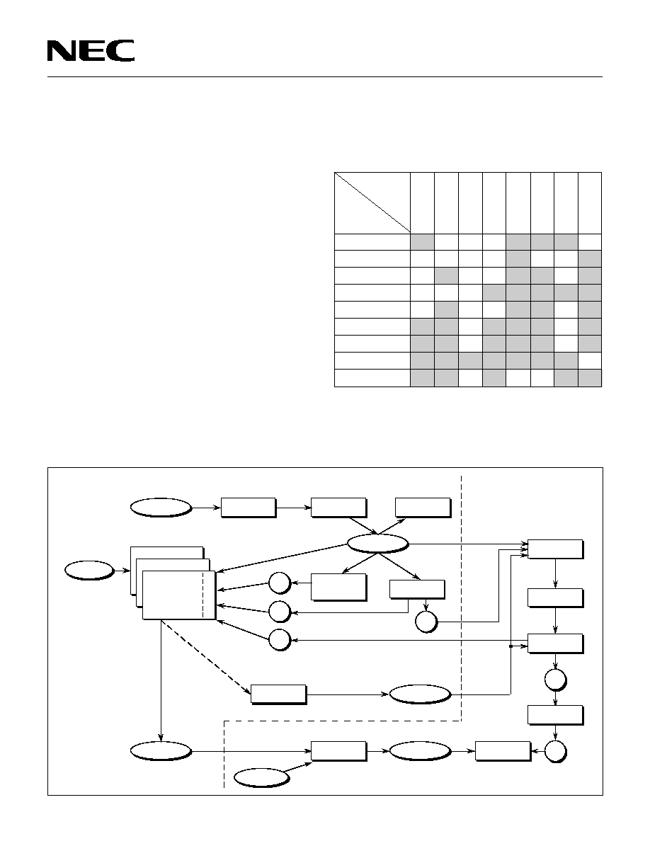
Table 2 CMOS-8 Package Options
Maximum
Package Dimensions
Master Slice µPD65xxx
I/O Pins
Body Size
Pitch
Height
-823
-825
-826
-828
-830
-831
-832
-833
-835
-838
Plastic Quad Flatpack (PQFP)
120-pin
28 mm
®
0.8 mm
3.7 mm
A
A
A
A
A
A
A
A
A
A
136-pin
28 mm
®
0.65 mm 3.7 mm
A
A
A
A
A
A
A
A
A
A
160-pin
28 mm
®
0.65 mm 3.7 mm
D
D
A
A
A
A
A
A
A
A
160-pin (H/S)
28 mm
®
0.65 mm 3.2 mm
≠
D
D
D
D
D
D
D
D
≠
184-pin
32 mm
®
0.65 mm 3.2 mm
D
D
D
D
D
D
D
D
D
D
Plastic Quad Flatpack (PQFP-FP)
100-pin
14 mm
®
0.5 mm
1.45 mm
A
A
A
≠
≠
≠
≠
≠
≠
≠
120-pin
20 mm
®
0.5 mm
2.7 mm
A
A
A
A
A
A
A
A
≠
≠
144-pin
20 mm
®
0.5 mm
2.7 mm
A
A
A
A
A
A
A
A
≠
≠
160-pin
24 mm
®
0.5 mm
2.7 mm
D
A
A
A
A
A
A
A
A
≠
160-pin (H/S)
24 mm
®
0.5 mm
2.7 mm
≠
P
P
P
P
P
P
P
P
≠
176-pin
24 mm
®
0.5 mm
2.7 mm
D
D
A
A
A
A
A
A
A
≠
176-pin (H/S)
24 mm
®
0.5 mm
2.7 mm
≠
≠
D
D
D
D
D
D
D
≠
208-pin
28 mm
®
0.5 mm
3.2 mm
D
D
D
D
A
A
A
A
A
A
208-pin (H/S)
28 mm
®
0.5 mm
3.2 mm
≠
≠
≠
≠
D
D
D
D
D
D
240-pin
32 mm
®
0.5 mm
3.2 mm
D
D
D
D
D
A
A
A
A
A
256-pin
28 mm
®
0.4 mm
3.2 mm
D
D
D
D
D
A
A
A
A
A
272-pin
36 mm
®
0.5 mm
3.2 mm
D
D
D
D
D
A
A
A
A
A
304-pin
40 mm
®
0.5 mm
3.7 mm
D
D
D
D
D
D
A
A
A
A
Thin Quad Flatpack (TQFP) PRELIMINARY
80-pin
12 mm
®
0.5 mm
1.05 mm
P
≠
≠
≠
≠
≠
≠
≠
≠
≠
100-pin
14 mm
®
0.5 mm
1.0 mm
P
P
P
≠
≠
≠
≠
≠
≠
≠
120-pin
14 mm
®
0.4 mm
1.0 mm
P
P
P
P
P
P
P
P
≠
≠
144-pin
20 mm
®
0.5 mm
1.4 mm
P
P
P
P
P
P
P
P
≠
≠
160-pin
24 mm
®
0.5 mm
1.4 mm
P
P
P
P
P
P
P
P
P
≠
176-pin
24 mm
®
0.5 mm
1.4 mm
P
P
P
P
P
P
P
P
P
≠
208-pin
28 mm
®
0.5 mm
1.4 mm
P
P
P
P
P
P
P
P
P
P
Ceramic Pin Grid Array (CPGA)
72-pin 27.94 mm
®
100 mils
4.57 mm
A
A
A
A
A
A
A
A
A
A
132-pin
35.56 mm
®
100 mils
4.57 mm
A
A
A
A
A
A
A
A
A
A
176-pin
38.10 mm
®
100 mils
4.57 mm
D
D
D
A
A
A
A
A
A
A
208-pin
43.18 mm
®
100 mils
5.08 mm
D
D
D
D
A
A
A
A
A
A
280-pin
48.26 mm
®
100 mils
4.57 mm
D
D
D
D
D
D
A
A
A
A
364-pin
43.18 mm
®
50 mils
3.0 mm
≠
≠
≠
D
D
D
D
D
A
A
Ceramic Pin Grid Array (CPGA) Butt-Lead
288-pin
27.94 mm
®
50 mils
5.58 mm
D
D
D
D
D
D
D
D
D
D
528-pin
48.26 mm
®
50 mils
10.6 mm
≠
≠
≠
≠
≠
D
D
D
D
D
Notation: A = Available; P = Planned; D = In Development; "≠" = Unavailable; H/S = Heat Spreader.
Note: NEC reserves the right to alter the package plan based on the results of qualification. For current package availability, please contact
your local NEC Design Center.
CMOS-8LCX
8
their design effort at a higher level of abstraction, specify-
ing, modeling, and simulating their designs at a systems
level. This leaves the details of the gate-level implementa-
tion to the synthesis tools. After verification confirms the
design's functionality, designers are then free to explore
various functional and architectural trade-offs, and can
optimize chip performance while minimizing chip area. An
engineer can evaluate several architectures and select the
best solution before committing the design to silicon.
The more traditional method of design entry, schematic
capture, figure 5, is available with a wide variety of third-
party tools. The supported tools, described in Table 3,
provide the designer with a productive way to manage the
hierarchical elements of a CMOS-8 design, utilizing the
macro symbol library provided by NEC. For those design-
ers who are experienced and already well-versed with
graphical design entry, this provides an efficient migration
path for ASIC development.
One of the key benefits of NEC's ASIC design flow is that
post place-and-route simulation can be accomplished at
the customer's site, since NEC offers designers a choice of
simulators within the "golden simulator" category. Golden
simulator status means that upon receiving post place-
and-route simulation results from a customer, NEC can
then proceed directly to photomask production, bypassing
any additional post-simulation steps. This can save a lot of
time.
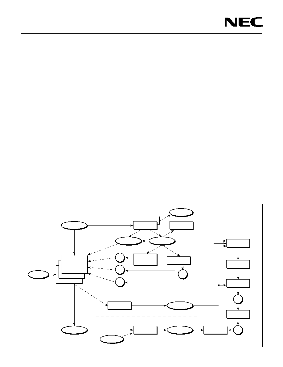
NEC's ASIC Design System
NEC supports its ASIC products with a comprehensive
CAD system that significantly reduces the time and ex-
pense usually associated with the development of semi-
custom devices. Designers can choose from today's most
popular third-party software tools, shown in the table on the
adjacent page. NEC's OpenCAD
Design System is a
front-end to back-end ASIC design package that merges
several advanced CAE/CAD tools into a single structure.
Designers can now choose a single CAE platform, or mix
and match tools from a variety of third-party vendors. The
design flow combines tools for floorplanning, logic synthe-
sis, automatic test generation, accelerated fault-grading,
full timing simulation, and advanced place-and-route algo-
rithms. This flexible design environment thereby ensures
accurate, on schedule designs.
There are two basic methods for design entry, the first is by
HDL specification, figure 4; the second is via schematic
capture, figure 5. Note that after the initial EDIF netlist is
generated, there is little difference in the basic design flow
for either method. Figure 6 shows the location of the
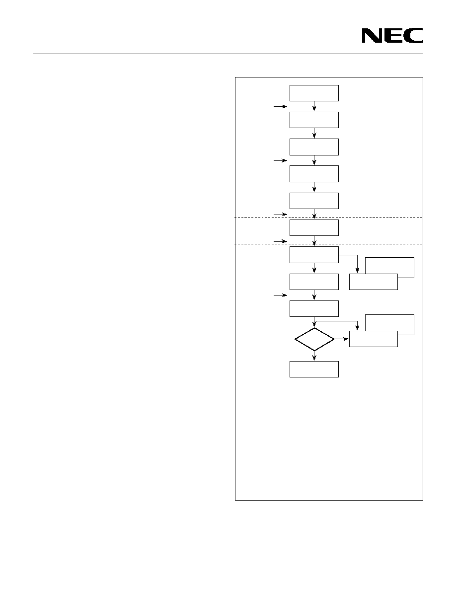
CrossCheck tools in the high-level design flow.
A top-down modeling methodology is possible using the
HDL specification approach. Designers can concentrate
Figure 4. HDL Specification Design Flow
HDL Netlist
EDIF 2.0.0
Netlist
DRC
SDF
SDF
Gate Level Sim.
Pre P&R Sim.
Post FP Sim.
Post P&R Sim.
Delay
Calculator
Floorplanner
DRC
Tester
CUSTOMER
NEC
Behavioral Sim.
ECO Option
ATPRG
DEF
Fault Simulation
Timing Analyzer
Test Synthesis
ATPG
Test Vector
ATPG
Test Vector
Simulator
Logic Synthesis
HDL
SDF
DEF
Place
CTS
Route
ES
Changed
Netlist
Test
Program
Fabrication
Test
Vector
Test Vector
Output
9
CMOS-8LCX
Sample design kits are available at no charge to qualified
users. A software license agreement is required. For more
information, contact your nearest NEC ASIC Design Cen-
ter, listed on the back of this data sheet.
Table 3 Third-Party Supported Tools
The floorplanner tool provides realistic estimates of wire
length by grouping hierarchical blocks into specific physical
locations on the chip. This minimizes critical path intercon-
nect delays for more accurate simulation. The floorplanner
also provides graphical I/O assignment capabilities and
generates a delay file for post-floorplanner simulation.
The ECO (Engineering Change Order) option in figures 4 and
5 allows the designer to make minor corrections in the design
without requiring an entirely new placement and routing of the
device. This tool improves turnaround time by ensuring that
relatively small changes, such as connectivity changes, will
not greatly impact the current design timing.
NEC also incorporates proprietary tools to facilitate the
design process. A single delay calculator is used for all
CAE platforms to ensure consistent timing and simulation
results. A comprehensive design rule check (DRC) pro-
gram reports design rule violations as well as chip utiliza-
tion statistics for the design netlist. The generated report
contains such information as net-count calculation, total
pin-count and cell-count use, and usage rate calculations.
Unused input pins, violations in pin naming conventions
and fan-out limits, are examples of the design rule viola-
tions reported by this program.
Synthesis
Synopsys
Cadence
U
Mentor
+
+
Viewlogic
Valid (Cadence)
+
IKOS
Zycad/NECplus
U
Intelligen
NEC
U
ATPG
Fault
Simulation
Place
and Route
Floorplanner
Static Timing
Analysis
Simulation
Tools
CAD
Company
Schematic
Entry
Key:
U
indicates "Golden Simulator" status.
indicates planned support-check with local Design Center for
exact availability.
+
indicates function is available via software library, and software
support is through third-party vendor.
Figure 5. Schematic-Based Design Flow
Post P
&R S
i m.
Post F P Sim.
Pre P&
R Sim.
EDI F Netlist
Writer
Symbol
Library
Simulator
Test Vector
Output
EDIF 2.0.0
Netlist
DRC
SDF
SDF
SDF
Dela y
Calculator
Floo rplanner
DEF
Place
DRC
CTS
Rou te
ES
Tester
CUSTOMER
NEC
ECO Optio n
Changed
Netlist
ATPRG
Test
Pro gram
DEF
Fabrication
Test
Vector
F unc
tiona
l Sim .
Schematic
Capture
Fault Simulation
Timing Analyzer
Megamacro
Test Vectors
CMOS-8LCX
10
CrossCheck Test Design Flow
The CMOS-8LCX (CrossCheck) ASICs makes use of a
unique test structure, called On-Chip Test EngineTM, that
allows testability to be incorporated into a CMOS-8LCX
design, using a process that is totally transparent to the
designer. This unique approach transfers the burden of
test development from the designer to NEC, where the
testability is incorporated automatically during the manu-
facturing phase of the device. A summary of the benefits
to CrossCheck Test are described below.
CrossCheck Test Benefits
®
Push-button automatic test pattern generation (ATPG)
®
No functional or initialization vectors required
®
Negligible performance impact
®
Netlist modifications not required
®
High fault coverage tests including stuck at,
bridging and manufacturing faults
®
Tests all design styles, including:
Synchronous single clock
Synchronous multiple gated clock
Asynchronous
®
Enhanced prototype diagnostic capability
Figure 6. Gate Array Design Flow with CrossCheck
TM On-Chip Test Engine is a trademark of CrossCheck Technology, Inc.
83RD-9079A
System Definition
Function and Logic
Design
Design Capture
(HDL/Schematic)
Synthesis and
Optimization
Design Analysis
Logic and Timing
Simulation
Placement and
Routing
Post-Layout
Simulation
Fabrication
Ship
Test
CrossCheck
CX-ProbeTM
Debug
Diagnostics
CrossCheck
CX-ArrayTestTM
Test Development
Level A
(Turn-Key)
Level B
(Netlist)
Level C
(Verified Netlist)
Note 1
Level D
(Qualified Simulation)
Level E
(Mask Tape)
NEC Environment
Design Environment
Notes :
(1) NEC supports the most popular CAD tools, including Cadence/
Valid, DAZIXÆ, IKOSÆ, Mentor GraphicsTM, SynopsysTM,
ViewlogicTM and ZycadTM for the NEC ASIC product line.
However, NEC does not support all CAD tools for all products.
Please contact your nearest NEC ASIC Design Center for
more information.
DAZIX is a registered trademark of DAZIX Daisy/Cadnetix Inc.
IKOS is a registered trademark of IKOS Systems, Inc.
Mentor Graphics is a trademark of Mentor Graphics Corporation
Synopsys is a trademark of Synopsys, Inc.
Viewlogic is a trademark of Viewlogic Systems, Inc.
Zycad is a trademark of Zycad Corporation
CX-ArrayTest is a trademark of CrossCheck Technologies, Inc.
CX-Probe is a trademark of CrossCheck Technologies, Inc.
11
CMOS-8LCX
Designing with CrossCheck
In using CrossCheck, the designer's only test consider-
ation is in the selection of a CMOS-8LCX base array. In
the design phase, the designer is free to use any pre-
ferred CAE tools and methodology supported by NEC.
This design freedom extends to the nature of the design,
synchronous or asynchronous, as shown in figure 4, where
the CMOS-8LCX gate array design flow with the
CrossCheck solution is illustrated. During simulation the
designer uses NEC's CrossCheck library. The only input
to test development is the netlist that is sent to NEC for
manufacturing CMOS-8LCX devices.
When the design is placed and routed, NEC automati-
cally connects the On-Chip Test Engine to the circuit
design. The test structure affords massive observability
and controllability of the design even though the CMOS-
8LCX looks exactly like a conventional ASIC. The con-
nections of the test structures have a negligible perfor-
mance impact on the design and require no modification
to the user's netlist.
NEC uses the CX-ArrayTestTM software to automatically
generate high fault coverage test patterns. The test devel-
opment process requires only the design netlist and place-
ment information. There is no need for designer-supplied
functional or initialization vectors, a significant benefit. CX-
ArrayTest software performs design analysis, ATPG, and
fault grading. The CX-ProbeTM, a software program devel-
oped by CrossCheck Technology, uses the on-chip test
structures to automate prototype debug and diagnostics.
With these tools, CMOS-8LCX gate arrays with the embed-
ded test solution resolve three of the key parameters for
testing the quality of ASICs: high fault coverage, rapid
failure analysis and time-to-market.
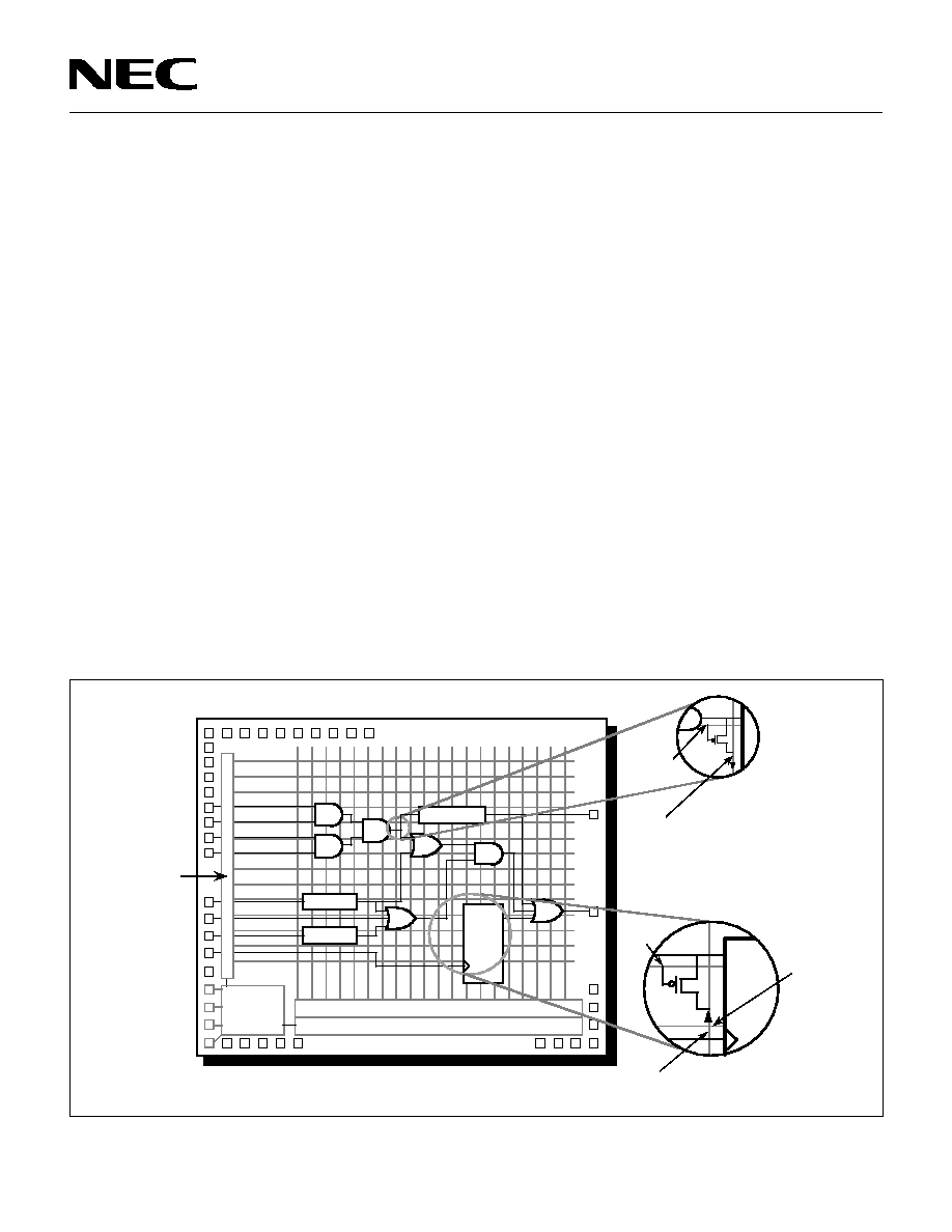
Embedded Test Structures
In the CMOS-8LCX, the test structure is embedded di-
rectly in the base array, as shown in figure 5. The On-
Chip Test Engine consists of a grid of sense transistors,
which provide massive observability and which are trans-
parent to the designer. An address matrix of probe and
sense lines select and control the node under test. A test
controller then manages the address matrix and acti-
vates the sense transistors. The small transistor used
has a negligible impact on the overall performance of the
gate array. There is one observation point for each four
transistors or gate.
TM CX-Probe and CX-ArrayTest are trademarks of CrossCheck Tech-
nology, Inc.
Figure 5. CMOS-8LCX CrossCheck On-Chip Test Engine
83FM-9078B
F/F
F/F
Probe Line
Address
Decoder
Drivers
IEEE 1149.1-
compatible
Test Bus
Test
Electronics
Controller
Data Register
Sense Line Driver/Receivers
Shift/LFSR Modes
Probe
Line
Sense Line
Test Data
Line
Probe
Line
Observation
Test
Point
Probe
Line for
Data
Injection
CrossCheck
Controllability
Latch
CMOS-8LCX
12
Table 4 Typical Fault Coverage with CX-
ArrayTest
The key to this on-chip test system is the patented
CrossCheck Controllability Latch (CCL), shown in figure
5, which allows fully automated test pattern generation
without modification to the user's netlist. The CCL uses
two embedded probe lines and a sense line to control the
latch data injection. Thus, the CCLs are not connected as
a synchronous chain. For this reason CX-ArrayTest soft-
ware can perform ATPG on asynchronous circuitry. The
CCL implementation has negligible impact on perfor-
mance.
Test Controller
The on-chip test electronics controller, shown in figure 5,
performs four major functions:
®
Interface to the CrossCheck Test Access Port
®
Test vector generation
®
Signature generation
®
On-Chip Test Engine self-test
Access to the On-Chip Test Engine is through
CrossCheck's Test Access Port. This test bus, compat-
ible with IEEE 1149.1, interfaces with automatic test
equipment (ATE). The ATE sends instructions and data
to the on-chip controller and in return receives test re-
sults from it. The On-Chip Test Engine produces test
vectors on the chip acting on instructions and/or data re-
ceived from the CX-ArrayTest software. This compatibil-
ity significantly reduces the ATE test vector memory re-
quirements for high fault coverage testing. To further re-
duce the amount of ATE vector memory used, the state
of the test points on the device are read and com-
pressed into a signature in the data register.
Fault Models
Because macrocells generally contain multiple test points,
defects within cells are detected. Traditional methods test
only the inputs and outputs of the macrocells, detecting
only the symptoms of a fault rather than the fault itself,
and often not detecting the fault at all. The CMOS-8LCX
CrossCheck test solution models nine different defect
types:
®
Stuck-at-faults:
Input stuck-at "1"
Output stuck-at "1"
Input stuck-at "0"
Output stuck-at "0"
®
Comprehensive manufacturing defects:
Shorted FET
Shorted intra-macro interconnect
Open FET
Open intra-macro interconnect
Shorted inter-macro networks
TM CX-Fault is a trademark of CrossCheck Technology, Inc.
The fault coverage that can be achieved is dependent
upon the design style used. Synchronous designs have
a single clock for the complete design. Gated clock de-
signs are generally synchronous but have several clocks
and flip-flop clocks that are gated by combinatorial logic.
Asynchronous is all other design styles. Asynchronous is
a design style often used in interface circuits, and is gen-
erally not testable with approaches such as
SCAN
.
The
CMOS-8LCX's ability to test asynchronous design is a
significant advantage of this test solution. Examples of
typical fault coverage using CMOS-8LCX are shown in
Table 4.
NEC uses CrossCheck's CX-FaultTM tool to analyze the
transistor-level descriptions of the macrocells to produce
a model library. The library contains the test generation
fault models that are used by the ATPG.
Automatic Test Pattern Generation
ATPG requires only the user netlist, placement file, and
the results of the test strategy developed from the netlist
analysis. CX-ArrayTest generates values for the test strat-
egy waveform template and avoids the hazard circuit
states. A full timing simulation is performed to determine
circuit stability after each vector is generated and ap-
plied. Simulating the On-Chip Test Engine allows cre-
ation of the signature of the internal circuit node states.
Faults are marked as detected only when the circuit is
stable and a signature is generated. The ATPG also
correctly handles any unavoidable hazard circuit states.
The CX-ArrayTest software monitors and reports fault
coverage, test time and vector length as it generates new
vectors.
The ATPG process continues until one of the user-defined
limits is reached, specifically fault coverage, number of test
vectors, test time, or elapsed ATPG processing time. At the
end of test generation, a set of vectors, including tests of the
On-Chip Test Engine, are packaged for translation onto
automatic test equipment.
Using the CrossCheck test solution allows automation of
the process of failure analysis, reducing diagnostics from
days or weeks to just hours.
Design Style
Stuck at Faults
Bridging Faults
Synchronous
> 98%
>99%
Multiple gated clocks
> 95%
>99%
Asynchronous
90% ≠ 95%
>98%
13
CMOS-8LCX
Block Library List
The CMOS-8L family offers a variety of blocks, including
gates, flip-flop circuits, and shift registers. The functions
of these blocks are designed to be compatible with those
of the CMOS-8, CMOS-7 and CMOS-6 families. In
addition, memory blocks such as RAM and ROM will be
provided, and low-power gates are available. The low-
power blocks are designed for gate count reduction; the
number of cells are fewer than that of the standard block,
contributing to lower power consumption and higher
efficiency. Another feature is the I/Os can directly interface
to 5V logic.
Block List
Block
I
OL
Description
Cells
Name
(mA)
Block
I
OL
Description
Cells
Name
(mA)
Interface Blocks
3V CMOS Input Buffers
FI01
3V CMOS input
-
1 (3)
FID1
3V CMOS input, 50 k
pull-down
-
1 (3)
FIU1
3V CMOS in, 50 k
pull-up
-
1 (3)
FIW1
3V CMOS in, 5 k
pull-up
-
1 (3)
FIS1
3V CMOS Schmitt input
-
1 (8)
FDS1
3V CMOS Schmitt input, 50 k
pull-down
-
1 (8)
FUS1
3V CMOS Schmitt input, 50 k
pull-up
-
1 (8)
FWS1 3V CMOS Schmitt input, 5 k
pull-up
-
1 (8)
FIB1
3V CMOS input, high fanout for clock driver
-
1 (24)
FDB1
3V CMOS input, high fanout for clock driver,
-
1 (24)
50 k
pull-down
FUB1
3V CMOS input, high fanout for clock driver,
-
1 (24)
50 k
pull-up
FWB1 3V CMOS input, high fanout for clock driver,
-
1 (24)
5 k
pull-up
3V CMOS Input Buffers without Protection Diode up to V
DD
FIA1
3V CMOS input
-
1 (3)
FDA1
3V CMOS input, 50 k
pull-down
-
1 (3)
FUA1
3V CMOS input, 50 k
pull-up
-
1 (3)
FWA1 3V CMOS input, 5 k
pull-up
-
1 (3)
FIE1
3V CMOS Schmitt input
-
1 (8)
FDE1
3V CMOS Schmitt input, 50 k
pull-down
-
1 (8)
FUE1
3V CMOS Schmitt input, 50 k
pull-up
-
1 (8)
FWE1 3V CMOS Schmitt input, 5 k
pull-up
-
1 (8)
FIH1
3V CMOS input, high fanout for clock driver
-
1 (24)
FDH1
3V CMOS input, high fanout for clock driver,
-
1 (24)
50 k
pull-down
FUH1
3V CMOS input, high fanout for clock driver,
-
1 (24)
50 k
pull-up
FWH1 3V CMOS input, high fanout for clock driver,
-
1 (24)
5 k
pull-up
5V CMOS Input Buffers
FIV1
5V CMOS input
-
1 (3)
FDV1
5V CMOS input, 50 k
pull-down
-
1 (3)
FIF1
5V CMOS Schmitt input
-
1 (8)
FDF1
5V CMOS Schmitt input, 50 k
pull-down
-
1 (8)
FIG1
5V CMOS input, high fanout for clock driver
-
1 (24)
FDG1
5V CMOS input, high fanout for clock driver,
-
1 (24)
50 k
pull-down
Interface Blocks (Cont.)
3V CMOS Output Buffers
FO0A
3V CMOS output
1.0
1 (4)
FO0B
3V CMOS output
2.0
1 (4)
FO09
3V CMOS output
3.0
1 (4)
FO04
3V CMOS output
6.0
1 (4)
FO01
3V CMOS output
9.0
1 (4)
FO02
3V CMOS output
12.0
1 (4)
FO03
3V CMOS output
18.0
1 (8)
FO06
3V CMOS output
24.0
1 (8)
FO0C
3V CMOS output
48.0
2 (8)
3V CMOS Slew-Rate Output Buffers
FE02
3V CMOS output, low noise
12.0
1 (3)
FE03
3V CMOS output, low noise
18.0
1 (3)
FE06
3V CMOS output, low noise
24.0
1 (3)
FE0C
3V CMOS output, low noise
48.0
2 (3)
5V CMOS Output Buffers
FV0A
5V CMOS output
1.0
1 (4)
FV0B
5V CMOS output
2.0
1 (4)
FV09
5V CMOS output
3.0
1 (4)
FV04
5V CMOS output
6.0
1 (4)
FV01
5V CMOS output
9.0
1 (8)
FV02
5V CMOS output
12.0
2 (8)
FV03
5V CMOS output
18.0
2 (8)
FV06
5V CMOS output
24.0
3 (8)
5V CMOS Slew-Rate Output Buffers
FW02
5V CMOS output, low noise
12.0
2 (3)
FW02
5V CMOS output, low noise
18.0
2 (3)
FW06
5V CMOS output, low noise
24.0
3 (3)
3V CMOS Three-State Output Buffers
B00T
3V CMOS output
3.0
1 (6)
B0DT
3V CMOS output, 50 k
pull-down
3.0
1 (6)
B0UT
3V CMOS output, 50 k
pull-up
3.0
1 (6)
B0WT 3V CMOS output, 5 k
pull-up
3.0
1 (6)
B00E
3V CMOS output
6.0
1 (6)
B0DE
3V CMOS output, 50 k
pull-down
6.0
1 (6)
B0UE
3V CMOS output, 50 k
pull-up
6.0
1 (6)
B0WE 3V CMOS output, 5 k
pull-up
6.0
1 (6)
B008
3V CMOS output
9.0
1 (6)
B0D8
3V CMOS output, 50 k
pull-down
9.0
1 (6)
B0U8
3V CMOS output, 50 k
pull-up
9.0
1 (6)
B0W8 3V CMOS output, 5 k
pull-up
9.0
1 (6)
B007
3V CMOS output
12.0
1 (6)
B0D7
3V CMOS output, 50 k
pull-down
12.0
1 (6)
B0U7
3V CMOS output, 50 k
pull-up
12.0
1 (6)
B0W7 3V CMOS output, 5 k
pull-up
12.0
1 (6)
B009
3V CMOS output
18.0
1 (9)
B0D9
3V CMOS output, 50 k
pull-down
18.0
1 (9)
B0U9
3V CMOS output, 50 k
pull-up
18.0
1 (9)
B0W9 3V CMOS output, 5 k
pull-up
18.0
1 (9)
B00H
3V CMOS output
24.0
1 (9)
B0DH 3V CMOS output, 50 k
pull-down
24.0
1 (9)
B0UH 3V CMOS output, 50 k
pull-up
24.0
1 (9)
B0WH 3V CMOS output, 5 k
pull-up
24.0
1 (9)
Note: Number of internal cells required is shown in parentheses.

CMOS-8LCX
14
Block
I
OL
Description
Cells
Name
(mA)
Block
I
OL
Description
Cells
Name
(mA)
Interface Blocks (Cont.)
Interface Blocks (Cont.)
Note: Number of internal cells required is shown in parentheses.
* Indicates I
OH
3V CMOS Three-State Output Buffers (Cont.)
B00J
3V CMOS output
48.0
2 (9)
B0DJ
3V CMOS output, 50 k
pull-down
48.0
2 (9)
B0UJ
3V CMOS output, 50 k
pull-up
48.0
2 (9)
B0WJ
3V CMOS output, 5 k
pull-up
48
2 (9)
3V CMOS Slew-Rate Three-State Output Buffers
BE07
3V CMOS output
12.0
1 (5)
BED7
3V CMOS output, 50 k
pull-down
12.0
1 (5)
BEU7
3V CMOS output, 50 k
pull-up
12.0
1 (5)
BEW7 3V CMOS output, 5 k
pull-up
12.0
1 (5)
BE09
3V CMOS output
18.0
1 (5)
BED9
3V CMOS output, 50 k
pull-down
18.0
1 (5)
BEU9
3V CMOS output, 50 k
pull-up
18.0
1 (5)
BEW9 3V CMOS output, 5 k
pull-up
18.0
1 (5)
BE0H
3V CMOS output
24.0
1 (5)
BEDH 3V CMOS output, 50 k
pull-down
24.0
1 (5)
BEUH 3V CMOS output, 50 k
pull-up
24.0
1 (5)
BEWH 3V CMOS output, 5 k
pull-up
24.0
1 (5)
BE0J
3V CMOS output
48.0
2 (5)
BEDJ
3V CMOS output, 50 k
pull-down
48.0
2 (5)
BEUJ
3V CMOS output, 50 k
pull-up
48.0
2 (5)
BEWJ 3V CMOS output, 5 k
pull-down
48.0
2 (5)
5V CMOS Three-State Output Buffers
BV0Q
5V CMOS output
1.0
1 (16)
BVDQ 5V CMOS output, 50 k
pull-down
1.0
1 (16)
BV0M 5V CMOS output
2.0
1 (16)
BVDM 5V CMOS output, 50 k
pull-down
2.0
1 (16)
BV0T
5V CMOS output
3.0
1 (16)
BVDT 5V CMOS output, 50 k
pull-down
3.0
1 (16)
BVOE 5V CMOS output
6.0
1 (16)
BVDE 5V CMOS output, 50 k
pull-down
6.0
1 (16)
BV08
5V CMOS output
9.0
1 (19)
BVD8
5V CMOS output, 50 k
pull-down
9.0
1 (19)
BV07
5V CMOS output
12.0
2 (19)
BVD7
5V CMOS output, 50 k
pull-down
12.0
2 (19)
BV09
5V CMOS output
18.0
2 (19)
BVD9
5V CMOS output, 50 k
pull-down
18.0
2 (19)
BV0H
5V CMOS output
24.0
3 (19)
BVDH 5V CMOS output, 50 k
pull-down
24.0
3 (19)
5V CMOS Slew-Rate Three-State Output Buffers
BY07
5V CMOS output
12.0 2 (15)
BYD7
5V CMOS output, 50 k
pull-down
12.0 2 (15)
BY09
5V CMOS output
18.0 2 (15)
BYD9
5V CMOS output, 50 k
pull-down
18.0 2 (15)
BY0H
5V CMOS ouputt
24.0 3 (15)
BYDH 5V CMOS output, 50 k
pull-down
24.0 3 (15)
3V CMOS Open Drain Output Buffers
EXTH 3V N-ch open drain
3.0
1 (4)
EXUH 3V N-ch open drain, 50 k
pull-up
3.0
1 (4)
EXWH 3V N-ch open drain, 5 k
pull-up
3.0
1 (4)
EXTJ
3V N-ch open drain
6.0
1 (4)
EXUJ
3V N-ch open drain, 50 k
pull-up
6.0
1 (4)
EXWJ 3V N-ch open drain, 5 k
pull-up
6.0
1 (4)
3V CMOS Open Drain Output Buffers (Cont.)
EXT1
3V N-ch open drain
9.0
1 (4)
EXT3
3V N-ch open drain, 50 k
pull-up
9.0
1 (4)
EXW3 3V N-ch open drain, 5 k
pull-up
9.0
1 (4)
EXT9
3V N-ch open drain
12.0
1 (4)
EXTB
3V N-ch open drain, 50 k
pull-up
12.0
1 (4)
EXWB 3V N-ch open drain, 5 k
pull-up
12.0
1 (4)
EXT5
3V N-ch open drain
18.0
1 (8)
EXT7
3V N-ch open drain, 50 k
pull-up
18.0
1 (8)
EXW7 3V N-ch open drain, 5 k
pull-up
18.0
1 (8)
EXTD 3V N-ch open drain
24.0
1 (8)
EXTF
3V N-ch open drain, 50 k
pull-up
24.0
1 (8)
EXWF 3V N-ch open drain, 5 k
pull-up
24.0
1 (8)
EXTL
3V N-ch open drain
48.0
2 (2)
EXUL
3V N-ch open drain, 50 k
pull-up
48.0
2 (8)
EXWL 3V N-ch open drain, 5 k
pull-up
48.0
2 (8)
EXTQ 3V P-ch open drain
*3.0
1 (4)
EXDQ 3V P-ch open drain, 50 k
pull-down
*3.0
1 (4)
EXTR 3V P-ch open drain
*6.0
1 (4)
EXDR 3V P-ch open drain, 50 k
pull-down
*6.0
1 (4)
EXT2
3V P-ch open drain
*9.0
1 (4)
EXT4
3V P-ch open drain, 50 k
pull-down
*9.0
1 (4)
EXTA
3V P-ch open drain
*12.0
1 (4)
EXTC 3V P-ch open drain, 50 k
pull-down
*12.0
1 (4)
EXT6
3V P-ch open drain
*18.0
1 (4)
EXT8
3V P-ch open drain, 50 k
pull-down
*18.0
1 (4)
EXTE
3V P-ch open drain
*24.0
1 (8)
EXTG 3V P-ch open drain, 50 k
pull-down
*24.0
1 (8)
EXTS
3V P-ch open drain
*48.0
2 (8)
EXDS 3V P-ch open drain, 50 k
pull-down
*48.0
2 (8)
3V CMOS Slew-Rate Open Drain Output Buffers
EET9
3V N-ch open drain
12.0
1 (2)
EETB
3V N-ch open drain, 50 k
pull-up
12.0
1 (2)
EEWB 3V N-ch open drain, 50 k
pull-up
12.0
1 (2)
EET5
3V N-ch open drain
18.0
1 (2)
EET7
3V N-ch open drain, 50 k
pull-up
18.0
1 (2)
EEW7 3V N-ch open drain, 5 k
pull-up
18.0
1 (2)
EETD 3V N-ch open drain
24.0
1 (2)
EETF
3V N-ch open drain, 50 k
pull-up
24.0
1 (2)
EEWF 3V N-ch open drain, 5 k
pull-up
24.0
1 (2)
EETL
3V N-ch open drain
48.0
2 (2)
EEUL
3V N-ch open drain, 50 k
pull-up
48.0
2 (2)
EEWL 3V N-ch open drain, 5 k
pull-up
48.0
2 (2)
EETA
3V P-ch open drain
*12.0
1 (2)
EETC 3V P-ch open drain, 50 k
pull-down
*12.0
1 (2)
EET6
3V P-ch open drain
*18.0
1 (2)
EET8
3V P-ch open drain, 50 k
pull-down
*18.0
1 (2)
EETE
3V P-ch open drain
*24.0
1 (2)
EETG 3V P-ch open drain, 50 k
pull-down
*24.0
1 (2)
EETS
3V P-ch open drain
*48.0
2 (2)
EEDS 3V P-ch open drain, 50 k
pull-down
*48.0
2 (2)
15
CMOS-8LCX
Block
I
OL
Description
Cells
Name
(mA)
Block
I
OL
Description
Cells
Name
(mA)
Interface Blocks (Cont.)
5V CMOS Open Drain Output Buffers
EVTH 5V N-ch open drain
3.0
1 (4)
EVTJ
5V N-ch open drain
6.0
1 (4)
EVT1
5V N-ch open drain
9.0
1 (8)
EVT9
5V N-ch open drain
12.0
1 (8)
EVT5
5V N-ch open drain
18.0
2 (8)
EVTD 5V N-ch open drain
24.0
2 (8)
5V CMOS Slew-Rate Output Buffers
EYT9
5V N-ch open drain
12.0
1 (2)
EYT5
5V N-ch open drain
18.0
2 (2)
EYTD 5V N-ch open drain
24.0
2 (2)
3V CMOS Bi-Directional Output Buffers
B00U
CMOS input, CMOS 3-state output
3.0
1 (9)
B0DU CMOS input, CMOS 3-state out, 50 k
pull-down
3.0
1 (9)
B0UU CMOS input, CMOS 3-state out, 50 k
pull-up
3.0
1 (9)
B0WU CMOS input, CMOS 3-state out, 5 k
pull-up
3.0
1 (9)
B00C
CMOS input, CMOS 3-state output
6.0
1 (9)
B0DC CMOS input, CMOS 3-state out, 50 k
pull-down
6.0
1 (9)
B0UC CMOS input, CMOS 3-state out, 50 k
pull-up
6.0
1 (9)
B0WC CMOS input, CMOS 3-state out, 5 k
pull-up
6.0
1 (9)
B003
CMOS inut, CMOS 3-state output
9.0
1 (8)
B0D3
CMOS input, CMOS 3-state out, 50 k
pull-down
9.0
1 (8)
B0U3
CMOS input, CMOS 3-state out, 50 k
pull-up
9.0
1 (8)
B0W3 CMOS in, CMOS 3-state out, 5 k
pull-up
9.0
1 (8)
B001
CMOS input, CMOS 3-state out
12.0
1 (9)
B0D1
CMOS input, CMOS 3-state out, 50 k
pull-down
12.0
1 (9)
B0U1
CMOS input, CMOS 3-state out, 50 k
pull-up
12.0
1 (9)
B0W1 CMOS input, CMOS 3-state out, 5 k
pull-up
12.0
1 (9)
B005
CMOS input, CMOS 3-state out
18.0 1 (12)
B0D5
CMOS input, CMOS 3-state out, 50 k
pull-down
18.0 1 (12)
B0U5
CMOS input, CMOS 3-state out, 50 k
pull-up
18.0 1 (12)
B0W5 CMOS input, CMOS 3-state out, 5 k
pull-up
18.0 1 (12)
B00F
CMOS input, CMOS 3-state out
24.0 1 (12)
B0DF
CMOS input, CMOS 3-state out, 50 k
pull-down
24.0 1 (12)
B0UF
CMOS input, CMOS 3-state out, 50 k
pull-up
24.0 1 (12)
B0WF CMOS input, CMOS 3-state out, 5 k
pull-up
24.0 1 (12)
B00W CMOS input, CMOS 3-state output
48.0 2 (12)
B0DW CMOS input, CMOS 3-state output,
48.0 2 (12)
50 k
pull-down
B0UW CMOS input, CMOS 3-state out,
48.0 2 (12)
50 k
pull-up resistor
B0WW CMOS input, CMOS 3-state output,
48.0 2 (12)
5 k
pull-up resistor
BSIU
CMOS Schmitt input, CMOS 3-state ouput
3.0 1 (14)
BSDU CMOS Schmitt input, CMOS 3-state output,
3.0 1 (14)
50 k
pull-down
BSUU CMOS Schmitt input, CMOS 3-state out,
3.0 1 (14)
50 k
pull-up
BSWU CMOS Schmitt input, CMOS 3-state output,
3.0 1 (14)
5 k
pull-up
BSIC
CMOS Schmitt input, CMOS 3-state output
6.0 1 (14)
BSDC CMOS Schmitt input, CMOS 3-state output,
6.0 1 (14)
50 k
pull-down
BSUC CMOS Schmitt input, CMOS 3-state output,
6.0 1 (14)
50 k
pull-up
BSWC CMOS Schmitt input, CMOS 3-state output,
6.0 1 (14)
5 k
pull-up
Interface Blocks (Cont.)
3V CMOS Bi-Directional Output Buffers
BSI3
CMOS Schmitt input, CMOS 3-state output
9.0 1 (14)
BSD3
CMOS Schmitt input, CMOS 3-state output,
9.0 1 (14)
50 k
pull-down
BSU3
CMOS Schmitt input, CMOS 3-state output,
9.0 1 (14)
50 k
pull-up
BSW3 CMOS Schmitt input, CMOS 3-state output,
9.0 1 (14)
5 k
pull-up
3V CMOS Three-State I/O Buffers
BSI1
CMOS Schmitt input, CMOS 3-state output
12.0 1 (14)
BSD1
CMOS Schmitt input, CMOS 3-state output,
12.0 1 (14)
50 k
pull-down
BSU1
CMOS Schmitt input, CMOS 3-state output,
12.0 1 (14)
50 k
pull-up
BSW1 CMOS Schmitt input, CMOS 3-state output,
12.0 1 (14)
5 k
pull-up
BSI5
CMOS Schmitt input, CMOS 3-state output
18.0 1 (17)
BSD5
CMOS Schmitt input, CMOS 3-state output,
18.0 1 (17)
50 k
pull-down
BSU5
CMOS Schmitt input, CMOS 3-state output,
18.0 1 (17)
50 k
pull-up
BSW5 CMOS Schmitt input, CMOS 3-state output,
18.0 1 (17)
5 k
pull-up
BSIF
CMOS Schmitt input, CMOS 3-state output
24.0 1 (17)
BSDF CMOS Schmitt input, CMOS 3-state output,
24.0 1 (17)
50 k
pull-down
BSUF
CMOS Schmitt input, CMOS 3-state output,
24.0 1 (17)
50 k
pull-up
BSWF CMOS Schmitt input, CMOS 3-state output,
24.0 1 (17)
5 k
pull-up
BSIW
CMOS Schmitt input, CMOS 3-state output
48.0 2 (17)
BSDW CMOS Schmitt input, CMOS 3-state output,
48.0 2 (17)
50 k
pull-down
BSUW CMOS Schmitt input, CMOS 3-state output,
48.0 2 (17)
50 k
pull-up
BSWW CMOS Schmitt input, CMOS 3-state output,
48.0 2 (17)
5 k
pull-up
3V CMOS Slew-Rate Three-State Output Buffers
BE01
CMOS input, CMOS 3-state output
12.0
1 (8)
BED1
CMOS input, CMOS 3-state output, 50 k
pull-dn
12.0
1 (8)
BEU1
CMOS input, CMOS 3-state output, 50 k
pull-up
12.0
1 (8)
BEW1 CMOS input, CMOS 3-state output, 5 k
pull-up
12.0
1 (8)
BE05
CMOS input, CMOS 3-state output
18.0
1 (8)
BED5
CMOS input, CMOS 3-state output, 50 k
pull-dn
18.0
1 (8)
BEU5
CMOS input, CMOS 3-state output, 50 k
pull-up
18.0
1 (8)
BEW5 CMOS input, CMOS 3-state output, 5 k
pull-up
18.0
1 (8)
BE0F
CMOS input, CMOS 3-state output
24.0
1 (8)
BEDF CMOS input, CMOS 3-state output, 50 k
pull-dn
24.0
1 (8)
BEUF CMOS input, CMOS 3-state output, 50 k
pull-up
24.0
1 (8)
BEWF CMOS input, CMOS 3-state output, 5 k
pull-up
24.0
1 (8)
BE0W CMOS input, CMOS 3-state output
48.0
2 (8)
BEDW CMOS input, CMOS 3-state output, 50 k
pull-dn
48.0
2 (8)
BEUW CMOS input, CMOS 3-state output, 50 k
pull-up
48.0
2 (8)
BEWW CMOS input, CMOS 3-state output, 5 k
pull-up
48.0
2 (8)
Note: Number of internal cells required is shown in parentheses.

CMOS-8LCX
16
Block
I
OL
Description
Cells
Name
(mA)
Block
I
OL
Description
Cells
Name
(mA)
BFI1
CMOS Schmitt input, CMOS 3-state output,
12.0 1 (13)
BFD1
CMOS Schmitt input, CMOS 3-state output,
12.0 1 (13)
50 k
pull-down
BFU1
CMOS Schmitt input, CMOS 3-state output,
12.0 1 (13)
50 k
pull-up
BFW1 CMOS Schmitt input, CMOS 3-state output,
12.0 1 (13)
5 k
pull-up
BFI5
CMOS Schmitt input, CMOS 3-state output
18.0 1 (13)
BFD5
CMOS Schmitt input, CMOS 3-state output,
18.0 1 (13)
50 k
pull-down
BFU5
CMOS Schmitt input, CMOS 3-state output,
18.0 1 (13)
50 k
pull-up
BFW5 CMOS Schmitt input, CMOS 3-state output,
18.0 1 (13)
5 k
pull-up
BFIF
CMOS Schmitt input, CMOS 3-state output,
24.0 1 (13)
BFDF
CMOSSchmitt input, CMOS 3-state output,
24.0 1 (13)
50 k
pull-down
BFUF
CMOS Schmitt input, CMOS 3-state output,
24.0 1 (13)
50 k
pull-up
BFWF CMOS Schmitt input, CMOS 3-state output,
24.0 1 (13)
5 k
pull-up
BFIW
CMOS Schmitt input, CMOS 3-state output,
48.0 2 (13)
BFDW CMOS Schmitt input, CMOS 3-state output,
48.0 2 (13)
50 k
pull-down
BFUW CMOS Schmitt input, CMOS 3-state output,
48.0 2 (13)
50 k
pull-up
BFWW CMOS Schmitt input, CMOS 3-state output,
48.0 2 (13)
5 k
pull-up
5V CMOS Bi-Directional Output Buffers
BW0X 5V CMOS input / CMOS 3-state output
1.0 1 (19)
BWDX 5V CMOS input / CMOS 3-state output,
1.0 1 (19)
with 50K
pull-down
BW0K 5V CMOS input / CMOS 3-state output
2.0 1 (19)
BWDK 5V CMOS input / CMOS 3-state output,
2.0 1 (19)
with 50K
pull-down
BW0U 5V CMOS input / CMOS 3-state output
3.0 1 (19)
BWDU 5V CMOS input / CMOS 3-state output,
3.0 1 (19)
with 50K
pull-down
BW0C 5V CMOS input / CMOS 3-state output
6.0 1 (19)
BWDC 5V CMOS input / CMOS 3-state output,
6.0 1 (19)
with 50K
pull-down
BW03 5V CMOS input / CMOS 3-state output
9.0 1 (22)
BWD3 5V CMOS input / CMOS 3-state output,
9.0 1 (22)
with 50K
pull-down
BW01 5V CMOS input / CMOS 3-state output
12.0 2 (22)
BWD1 5V CMOS input / CMOS 3-state output,
12.0 2 (22)
with 50K
pull-down
BW05 5V CMOS input / CMOS 3-state output
18.0 2 (22)
BWD5 5V CMOS input/ CMOS 3-state output,
18.0 2 (22)
with 50K
pull-down
BW0F 5V CMOS input/ CMOS 3-state output,
24.0 3 (22)
BWDF 5V CMOS input/ CMOS 3-state output,
24.0 3 (22)
with 50K
pull-down
3V CMOS Slew-Rate Three-State Output Buffers (Cont.)
BKIX
5V CMOS Schmitt input, CMOS 3-state output
1.0 1 (24)
BKDX
5V CMOS Schmitt input,
1.0 1 (24)
CMOS 3-state output, 50 k
pull-down
BKIK
5V CMOS Schmitt input, CMOS 3-state output
2.0 1 (24)
BKDK
5V CMOS Schmitt input,
2.0 1 (24)
CMOS 3-state output, 50k
pull-down
BKIU
5V CMOS Schmitt input, CMOS 3-state output
3.0 1 (24)
BKDU 5V CMOS Schmitt input,
3.0 1 (24)
CMOS 3-state output, 50 k
pull-down
BKIC
5V CMOS Schmitt in, CMOS 3-state output
6.0 1 (24)
BKDC 5V CMOS Schmitt input,
6.0 1 (24)
CMOS 3-state out, 50 k
pull-down resistor
BKI3
5V CMOS Schmitt input, CMOS 3-state output
9.0 1 (27)
BKD3
5V CMOS Schmitt input,
9.0 1 (24)
CMOS 3-state output, 50 k
pull-down
BKI1
5V CMOS Schmitt input, CMOS 3-state output
12.0 2 (27)
BKD1
5V CMOS Schmitt input,
12.0 2 (27)
CMOS 3-state output, 50k
pull-down
BKI5
5V CMOS Schmitt input, CMOS 3-state output
18.0 2 (27)
BKD5
5V CMOS Schmitt input,
18.0 2 (27)
CMOS 3-state output, 50 k
pull-down resistor
BKIF
5V CMOS Schmitt input, CMOS 3-state output
24.0 3 (27)
BKDF 5V CMOS Schmitt input,
24.0 3 (27)
CMOS 3-state output, 50 k
pull-down
5V CMOS Slew-Rate Bi-Directional Output Buffers
BX01
5V CMOS input / CMOS 3-state output
12.0 2 (18)
BXD1
5V CMOS input / CMOS 3-state output,
12.0 2 (18)
with 50K
pull-down
BX05
5V CMOS input / CMOS 3-state output
18.0 2 (18)
BXD5
5V CMOS input / CMOS 3-state output,
18.0 2 (18)
with 50K
pull-down
BX0F
5V CMOS input / CMOS 3-state output
24.0 3 (18)
BXDF 5V CMOS input / CMOS 3-state output,
24.0 3 (18)
with 50K
pull-down
BZI1
5V CMOS Schmitt input, CMOS 3-state output
12.0 2 (23)
BZD1
5V CMOS Schmitt in, CMOS 3-state
12.0 2 (23)
output, 50k
pull-down
BZI5
5V CMOS Schmitt input, CMOS 3-state output
18.0 2 (23)
BZD5
5V CMOS Schmitt input, CMOS 3-state
18.0 2 (23)
output, 50 k
pull-down
BZ1F
5V CMOS Schmitt input, CMOS 3-state output
24.0 3 (23)
BZDF
5V CMOS Schmitt input, CMOS 3-state
24.0 3 (23)
output, 50 k
pull-down
Interface Blocks (Cont.)
Interface Blocks (Cont.)
5V CMOS Bi-Directional Output Buffers (Cont.)
Note: Number of internal cells required is shown in parentheses.

17
CMOS-8LCX
Note: Number of internal cells required is shown in parentheses.
Interface Blocks
Block
Description
Cells
Name
Function Blocks ≠ Normal Power
Inverters
F101
Inverter (F/O = 17)
1
F102
Inverter (F/O = 37)
2
F103
Inverter (F/O = 60)
3
F104
Inverter (F/O = 92)
4
F108
Inverter (F/O = 160)
12
Buffers
F111
Non-inverting buffer (F/O = 17)
2
F112
Non-inverting buffer (F/O = 35)
3
F113
Non-inverting buffer (F/O = 54)
4
F114
Non-inverting buffer (F/O = 74)
5
F118
Non-inverting buffer (F/O = 180)
11
NOR Gates
F202
2-input NOR
2
F203
3-input NOR
3
F204
4-input NOR
4
F205
5-input NOR
5
F206
6-input NOR
5
F208
8-input NOR
7
F222
2-input NOR, power
4
F223
3-input NOR, power
6
F224
4-input NOR, power
8
OR Gates
F212
2-input OR
2
F213
3-input OR
3
F214
4-input OR
3
F215
5-input OR
5
F216
6-input OR
5
F232
2-input OR, power
3
F233
3-input OR, power
4
F234
4-input OR, power
4
NAND Gates
F302
2-input NAND
2
F303
3-input NAND
3
F304
4-input NAND
4
F305
5-input NAND
5
F306
6-input NAND
5
F308
8-input NAND
6
F322
2-input NAND, power
4
F323
3-input NAND, power
6
F324
4-input NAND, power
8
AND Gates
F312
2-input AND
2
F313
3-input AND
3
F314
4-input AND
3
F315
5-input AND
5
F316
6-input AND
5
F332
2-input AND, power
3
F333
3-input AND, power
4
F334
4-input AND, power
4
AND-NOR Gates
F421
2-wide 1-2-input AND-OR inverter
3
F422
3-wide 1-1-2-input AND-OR inverter
4
F423
2-wide 1-3-input AND-OR inverter
4
F424
2-wide 2-2-input AND-OR inverter
4
F425
3-wide 2-2-2-input AND-OR inverter
6
F426
2-wide 3-3-input AND-OR inverter
6
F429
4-wide 2-2-2-2-input AND-OR inverter
8
F442
2-wide 4-4-input AND-OR inverter
8
F462
3-wide 1-2-3-input AND-OR inverter
6
OR-NAND Gates
F431
2-wide 1-2-input OR-AND inverter
3
F432
3-wide 1-1-2-input OR-AND inverter
4
F433
2-wide 1-3-input OR-AND inverter
4
F434
2-wide 2-2-input OR-AND inverter
4
F435
2-wide 2-3-input OR-AND inverter
5
F436
2-wide 3-3-input OR-AND inverter
6
F454
4-wide 2-2-2-2-input OR-AND inverter
8
Clock Drivers
FCK1
Clock driver (F/O = 360)
40
FCK2
Clock driver (F/O = 720)
80
FCK3
Clock driver (F/O = 1080)
120
FCK4
Clock driver (F/O = 1440)
160
FCK5
Clock driver (F/O = 1800)
200
Exclusive OR Functions
F511
2-input Exclusive-OR
4
F512
2-input Exclusive-NOR
4
Parity Generators
F581
8-bit odd parity generator
19
F582
8-bit even parity generator
19
Adders
F521
1-bit full-adder
9
F523
4-bit binary full-adder
32
F526
Carry look-ahead generator
34
F527
4-bit full-adder
66
Miscellaneous
F091
H, L level generator
1
F093
Interface block for oscillator buffer
1
Three-state Buffers
F531
3-state buffer with enable
5
F532
3-state buffer with active low enable
5
Decoders
F561
2-to-4 decoder
10
F981
2-to-4 decoder with active low enable
13
F982
3-to-8 decoder with active low enable
26
Multiplexers
F569
8-to-1 multiplexer
18
F570
4-to-1 multiplexer
10
F571
2-to-1 multiplexer
6
F572
Quad 2-to-1 multiplexer
14
Block
Description
Cells
Name

CMOS-8LCX
18
Latches
F595
R-S latch
5
F601
D-latch
6
F602
D-latch with reset
6
F603
D-latch with reset low
7
F604
D-latch with active low gate (G)
6
F605
D-latch with active low gate (G), reset low
7
F901
4-bit D-latch, buffered output
20
F902
8-bit D-latch, buffered output
38
Flip-Flops
F596
Synchronous R-S F/F with set-reset
11
F611
D-F/F
8
F614
D-F/F with set-reset
10
F615
D-F/F with reset low
9
F616
D-F/F with set low
9
F617
D-F/F with set-reset low
10
F631
D-F/F active low clock
8
F637
D-F/F active low clock with set-reset low
10
F641
D-F/F, buffered output
8
F644
D-F/F with set-reset, buffered output
10
F647
D-F/F with set-reset low, buffered output
10
F661
D-F/F active low clock, buffered output
8
F667
D-F/F active low clock with set-reset low,
10
buffered output
F714
Toggle F/F with set-reset
9
F717
Toggle F/F with set-reset low
9
F737
Toggle low F/F with set-reset low
9
F744
Toggle F/F with set-reset, buffered output
9
F747
Toggle F/F with set-reset low, buffered output
9
F767
Toggle active low F/F with set-reset low,
9
buffered output
F771
J-K F/F, buffered output
10
F774
J-K F/F with set-reset, buffered output
12
F777
J-K F/F with set-reset low, buffered output
12
F781
J-K F/F active low clock, buffered output
10
F787
J-K F/F active low clock with set-reset low,
12
buffered output
F791
Toggle F/F with set-reset and toggle enable
12
F792
Toggle active low F/F with set-reset low and toggle
12
enable low
F922
4-bit D-F/F with reset
33
F924
4-bit D-F/F
28
Shift Registers
F911
4-bit shift register with reset
33
F912
4-bit serial/parallel shift register
35
F913
4-bit serial/parallel shift register with reset low
39
F914
4-bit shift register
28
F915
4-bit shift register w/direct load low, buffered output
44
Counters
F961
4-bit synchronous binary up counter with reset low,
52
load low, buffered output
F962
4-bit synchronous binary up counter with reset low
38
F963
4-bit presettable synchronous up/down binary counter
72
(dual clock with clear)
F964
4-bit presettable synchronous up/down binary counter
86
Comparator
F985
4-bit magnitude comparator
32
Scan
S000
Scan path D-F/F with set-reset
11
S002
Scan path D-F/F
9
S050
Scan path D-F/F with set-reset, hold
14
S052
Scan path D-F/F with hold
12
S100
Scan path J-K F/F with set-reset
14
S102
Scan path J-K F/F
12
S150
Scan path J-K F/F with set-reset, hold
17
S152
Scan path J-K F/F with hold
15
S201
Scan path D-latch with reset
12
S202
Scan path D-latch
11
S301
Scan path D-latch with reset
8
S302
Scan path D-latch
7
S999
Scan path 2-to-1 data selector
4
Delays
F130
Delay block (for monostable multivibrator)
8
F131
Delay gate
6
F132
Delay gate
1
Function Blocks ≠ Low Power
Inverter
L101
Inverter
1
Buffer
L111
Non-inverting buffer
1
NOR Gates
L202
2-input NOR
1
L203
3-input NOR
2
L204
4-input NOR
2
OR Gates
L212
2-input OR
2
L213
3-input OR
2
L214
4-input OR
3
NAND Gates
L302
2-input NAND
1
L303
3-input NAND
2
L304
4-input NAND
2
L305
5-input NAND
3
L306
6-input NAND
3
AND Gates
L312
2-input AND
2
L313
3-input AND
2
L314
4-input AND
3
AND-NOR Gates
L421
2-wide 1-2-input AND-OR inverter
2
L422
3-wide 1-1-2-input AND-OR inverter
2
L423
2-wide 1-3-input AND-OR inverter
2
L424
2-wide 2-2-input AND-OR inverter
2
Function Blocks ≠ Normal Power (Cont.)
Function Blocks ≠ Normal Power (Cont.)
Block
Description
Cells
Name
Block
Description
Cells
Name

19
CMOS-8LCX
Basic
Block
Description
BIST
Cells
RAM
AND-NOR Gates
L425
3-wide 2-2-2-input AND-OR inverter
3
L426
2-wide 3-3-input AND-OR inverter
3
L429
4-wide 2-2-2-2-input AND-OR inverter
4
L442
2-wide 4-4-input AND-OR inverter
4
L462
3-wide 1-2-3-input AND-OR inverter
3
OR-NAND Gates
L431
2-wide 1-2-input OR-AND inverter
2
L432
3-wide 1-1-2-input OR-AND inverter
2
L433
2-wide 1-3-input OR-AND inverter
2
L434
2-wide 2-2-input OR-AND inverter
2
L435
2-wide 2-3-input OR-AND inverter
3
L436
2-wide 3-3-input OR-AND inverter
3
L454
4-wide 2-2-2-2-input OR-AND inverter
4
Exclusive OR Functions
L511
2-input EX-OR
3
EX-NOR Gate
L512
2-input EX-NOR
3
Decoders
L561
2-to-4 decoder
6
L981
2-to-4 decoder with active low enable
8
L982
3-to-8 decoder with active low enable
17
Latches
L601
D-latch
3
L602
D-latch with reset
4
L603
D-latch with reset low
4
L604
D-latch with active low gates (G)
3
L605
D-latch with active low gates (G), reset low
4
L901
4-bit latch
10
L902
8-bit latch
18
Flip-Flops
L611
D-F/F
5
L614
D-F/F with set-reset
7
L617
D-F/F with set-reset low
7
L631
D-F/F with active low clock
5
L637
D-F/F with active low clock, set-reset low
7
L714
Toggle-F/F with set-reset
7
L717
Toggle-F/F with set-reset low
7
L737
Toggle active low F/F with set-reset low
7
L922
4-bit D-F/F with reset
23
L924
4-bit D-F/F
18
Multiplexer
L571
2-to-1 multiplexer
6
L572
Quad 2-to-1 multiplexer
10
Shift Registers
L911
4-bit shift register with reset
23
L912
4-bit serial/parallel shift register
23
L913
4-bit serial/parallel in shift register with reset low
27
L914
4-bit shift register
18
Function Blocks ≠ Low Power (Cont.)
RAM Memory Blocks
High-Speed Basic RAM Blocks - Hard Macros
KD49
Single-port RAM (32 word x 4 bit)
--
--
578
KD8B
Single-port RAM (64 word x 8 bit)
--
--
1712
KD8F
Single-port RAM (256 word x 8 bit)
--
--
6070
KDAB
Single-port RAM (64 word x 10 bit)
--
--
2020
KDAF
Single-port RAM (256 word x 10 bit)
--
--
7292
KE49
Dual-port RAM (32 word x 4 bit)
--
--
798
KE87
Dual-port RAM (16 word x 8 bit)
--
--
634
KE8B
Dual-port RAM (64 word x 8 bit)
--
--
2178
KE8F
Dual-port RAM (256 word x 8 bit)
--
--
6408
KEAB
Dual-port RAM (64 word x 10 bit)
--
--
2486
KEAF
Dual-port RAM (256 word x 10 bit)
--
--
7630
KE9H
Dual-port RAM (512 word x 9 bit)
--
--
12682
High-Speed Single Port RAM Blocks - Soft Macros
RJ49
Single-port RAM (32 word x 4 bit)
KD49 RU49
782
RJ4B
Single-port RAM (64 word x 4 bit)
KD49 RU4B
1389
RJ4D
Single-port RAM (128 word x 4 bit)
KD49 RU4D
2572
RJ4F
Single-port RAM (256 word x 4 bit)
KD49 RU4F
4940
RJ89
Single-port RAM (32 word x 8 bit)
KD49 RU89
1382
RJ8B
Single-port RAM (64 word x 8 bit)
KD8B RU8B
1964
RJ8D
Single-port RAM (128 word x 8 bit)
KD8B RU8D
3712
RJ8F
Single-port RAM (256 word x 8 bit)
KD8B RU8F
6354
RJ8H
Single-port RAM (512 word x 8 bit)
KD8B RU8H 12460
RJAB
Single-port RAM (64 word x 10 bit)
KDAB RUAB
2290
RJAD
Single-port RAM (128 word x 10 bit)
KDAB RUAD
4350
RJAF
Single-port RAM (256 word x 10 bit)
KDAB RUAF
7592
RJAH
Single-port RAM (512 word x 10 bit)
KDAB RUAH 14924
RJC9
Single-port RAM (32 word x 16 bit)
KD49 RUC9
2618
RJCB
Single-port RAM (64 word x 16 bit)
KD8B RUCB
3746
RJCD
Single-port RAM (128 word x 16 bit)
KD8B RUCD
7223
RJCF
Single-port RAM (256 word x 16 bit)
KD8B RUCF 12493
RJEB
Single-port RAM (64 word x 20 bit)
KDAB RUEB
4394
RJED
Single-port RAM (128 word x 20 bit)
KDAB RUED
8494
RJEF
Single-port RAM (256 word x 20 bit)
KDAB RUEF 14968
RJH9
Single-port RAM (32 word x 32 bit)
KD49 RUH9
5062
RJHB
Single-port RAM (64 word x 32 bit)
KD8B RUHB
7303
RJHD
Single-port RAM (128 word x 32 bit)
KD8B RUHD 14235
RJKB
Single-port RAM (64 word x 40 bit)
KDAB RUKB
8399
RJKD
Single-port RAM (128 word x 40 bit)
KDAB RUKD 16779
High-Speed Dual Port RAM Blocks - Soft Macros
RK49
Dual-port RAM (32 word x 4 bit)
KE49
RU49
1029
RK4B
Dual-port RAM (64 word x 4 bit)
KE49
RU4B
1866
RK4D
Dual-port RAM (128 word x 4 bit)
KE49
RU4D
3502
RK4F
Dual-port RAM (256 word x 4 bit)
KE49
RU4F
6768
RK87
Dual-port RAM (16 word x 8 bit)
KE87
RU87
885
RK89
Dual-port RAM (32 word x 8 bit)
KE49
RU89
1860
RK8B
Dual-port RAM (64 word x 8 bit)
KE8B RU8B
2463
RK8D
Dual-port RAM (128 word x 8 bit)
KE8B RU8D
4687
RK8F
Dual-port RAM (256 word x 8 bit)
KE8F RU8F
6733
RK8H
Dual-port RAM (512 word x 8 bit)
KE8F RU8H 13187
RKAB
Dual-port RAM (64 word x 10 bit)
KEAB RUAB
2787
RKAD
Dual-port RAM (128 word x 10 bit)
KEAB RUAD
5323
RKAF
Dual-port RAM (256 word x 10 bit)
KEAF RUAF
7971
RKAH
Dual-port RAM (512 word x 10 bit)
KEAF RUAH 15651
Block
Description
Cells
Name

CMOS-8LCX
20
RKC9
Dual-port RAM (32 word x 16 bit)
KE49
RUC9
3524
RKCB
Dual-port RAM (64 word x 16 bit)
KE8B
RUCB
4709
RKCD
Dual-port RAM (128 word x 16 bit)
KE8B
RUCD
9127
RKCF
Dual-port RAM (256 word x 16 bit)
KE8F
RUCF 13209
RKEB
Dual-port RAM (64 word x 20 bit)
KEAB
RUEB
5357
RKED
Dual-port RAM (128 word x 20 bit)
KEAB
RUED 10399
RKEF
Dual-port RAM (256 word x 20 bit)
KE49
RUH9 15256
RKH9
Dual-port RAM (32 word x 32 bit)
KE8B
RUHB
6849
RKHB
Dual-port RAM (64 word x 32 bit)
KE8B
RUHD
9198
RKHD
Dual-port RAM (128 word x 32 bit)
KE8B
RUHD 18004
RKKB
Dual-port RAM (64 word x 40 bit)
KEAB
RUKB 10494
RKKD
Dual-port RAM (128 word x 40 bit)
KEAB
RUKD 20548
High-Density Single-Port RAM Blocks - Soft Macros
RB4D
Single-port RAM (128 word x 4 bit)
K14D
RU4D
1315
RB4F
Single-port RAM (256 word x 4 bit)
K14D
RU4F
2423
RB4H
Single-port RAM (512 word x 4 bit)
K14D
RU4H
4610
RB4M
Single-port RAM (1K word x 4 bit)
K14D
RU4M
8986
RB4S
Single-port RAM (2K word x 4 bit)
K14D
RU4S
17754
RB4U
Single-port RAM (4K word x 4 bit)
K14D
RU4U 35172
RB8D
Single-port RAM (128 word x 8 bit)
K14D
RU8D
2472
RB8F
Single-port RAM (256 word x 8 bit)
K18F
RU8F
3978
RB8H
Single-port RAM (512 word x 8 bit)
K18F
RU8H
7711
RB8M
Single-port RAM (1K word x 8 bit)
K18M
RU8M 12523
RB8S
Single-port RAM (2K word x 8 bit)
K18M
RU8S
24770
RBAF
Single-port RAM (256 word x 10 bit)
K1AF
RUAF
4877
RBAH
Single-port RAM (512 word x 10 bit)
K1AF
RUAH
9495
RBAM
Single-port RAM (1K word x 10 bit)
K1AM
RUAM 15499
RBAS
Single-port RAM (2K word x 10 bit)
K1AM
RUAS 30710
RBCD
Single-port RAM (128 word x 16 bit)
K14D
RUCD
4657
RBCF
Single-port RAM (256 word x 16 bit)
K18F
RUCF
7744
RBCH
Single-port RAM (512 word x 16 bit)
K18F
RUCH 15188
RBCM
Single-port RAM (1K word x 16 bit)
K18M
RUCM 24801
RBEF
Single-port RAM (256 word x 20 bit)
K1AF
RUEF
9539
RBEH
Single-port RAM (512 word x 20 bit)
K1AF
RUEH 18756
RBEM
Single-port RAM (1K word x 20 bit)
K1AM
RUHM 30754
RBHD
Single-port RAM (128 word x 32 bit)
K14D
RUHD
9109
RBHF
Single-port RAM (256 word x 32 bit)
K18F
RUHF 15268
RBHH
Single-port RAM (512 word x 32 bit)
K18F
RUHH 30137
RBKF
Single-port RAM (256 word x 40 bit)
K1AF
RUKF 18861
RBKH
Single-port RAM (512 word x 40 bit)
K1AF
RUKH 37273
Basic
Block
Description
BIST
Cells
RAM
Memory Blocks (Cont.)
High-Speed RAM Blocks - Soft Macros (Cont.)
ROM Memory Blocks
Block
Description
Cells
ROM Blocks
J14D
128 word x 4 bit ROM
720
J14F
256 word x 4 bit ROM
1040
J14H
512 word x 4 bit ROM
1512
J14M
1K word x 4 bit ROM
2408
J14S
2K word x 4 bit ROM
3960
J14U
4K word x 4 bit ROM
6776
J18D
128 word x 8 bit ROM
1040
J18F
256 word x 8 bit ROM
1456
J18H
512 word x 8 bit ROM
2352
J18M
1K word x 8 bit ROM
3784
J18S
2K word x 8 bit ROM
6600
J18U
4K word x 8 bit ROM
11704
J18W
8K word x 8 bit ROM
21584
J1CD
128 word x 16 bit ROM
1456
J1CF
256 word x 16 bit ROM
2352
J1CH
512 word x 16 bit ROM
3696
J1CM
1K word x 16 bit ROM
6512
J1CS
2K word x 16 bit ROM
11400
J1CU
4K word x 16 bit ROM
21280
J1HF
256 word x 32 bit ROM
3696
J1HH
512 word x 32 bit ROM
6512
J1HM
1K word x 32 bit ROM
11248
J1HS
2K word x 32 bit ROM
21128
RAM Test (BIST)
RU49
32 word x 4 bit
RU4B
64 word x 4 bit
RU4D
128 word x 4 bit
RU4F
256 word x 4 bit
RU87
16 word x 8 bit
RU89
32 word x 8 bit
RU8B
64 word x 8 bit
RU8D
128 word x 8 bit
RU8F
256 word x 8 bit
RU8H
512 word x 8 bit
RUAB
64 word x 10 bit
RUAD
128 word x 10 bit
RUAF
256 word x 10 bit
RUAH
512 word x 10 bit
RUC9
32 word x 16 bit
RUCB
64 word x 16 bit
RUCD
128 word x 16 bit
RUCF
256 word x 16 bit
RUEB
64 word x 20 bit
RUED
128 word x 20 bit
RUEF
256 word x 20 bit
RUH9
32 word x 32 bit
RUHB
64 word x 32 bit
RUHD
128 word x 32 bit
RUKB
64 word x 40 bit
RUKD
128 word x 40 bit

21
CMOS-8LCX
Notes:

CMOS-8LCX
22
Notes:

23
CMOS-8LCX
Notes:
CMOS-8LCX
24
THIRD-PARTY DESIGN CENTERS
SOUTH CENTRAL/SOUTHEAST
∑ Koos Technical Services, Inc.
385 Commerce Way, Suite 101
Longwood, FL 32750
TEL 407-260-8727
FAX 407-260-6227
∑ Integrated Silicon Systems Inc.
2222 Chapel Hill Nelson Highway
Durham, NC 27713
TEL 919-361-5814
FAX 919-361-2019
NEC ASIC DESIGN CENTERS
SOUTH CENTRAL/SOUTHEAST
∑ 16475 Dallas Parkway, Suite 380
Dallas, TX 75248
TEL 972-250-4522
FAX 972-931-8680
∑ Research Triangle Park
2000 Regency Parkway, Suite 455
Cary, NC 27511
TEL
919-460-1890
FAX 919-469-5926
WEST
∑ 3033 Scott Boulevard
Santa Clara, CA 95054
TEL 408-588-5008
FAX 408-588-5017
∑ One Embassy Centre
9020 S.W. Washington Square Road,
Suite 400
Tigard, OR 97223
TEL 503-671-0177
FAX 503-643-5911
CORPORATE HEADQUARTERS
2880 Scott Boulevard
P.O. Box 58062
Santa Clara, CA 95052
TEL 408-588-6000
For literature, call toll-free 7 a.m. to 6 p.m. Pacific time: 1-800-366-9782
or FAX your request to: 1-800-729-9288
No part of this document may be copied or reproduced in any form or by any means without the prior written consent of NEC Electronics Inc.
(NECEL). The information in this document is subject to change without notice. ALL DEVICES SOLD BY NECEL ARE COVERED BY THE
PROVISIONS APPEARING IN NECEL TERMS AND CONDITIONS OF SALES ONLY. INCLUDING THE LIMITATION OF LIABILITY, WARRANTY,
AND PATENT PROVISIONS. NECEL makes no warranty, express, statutory, implied or by description, regarding information set forth herein
or regarding the freedom of the described devices from patent infringement. NECEL assumes no responsibility for any errors that may
appear in this document. NECEL makes no commitments to update or to keep current information contained in this document. The devices
listed in this document are not suitable for use in applications such as, but not limited to, aircraft control systems, aerospace equipment,
submarine cables, nuclear reactor control systems and life support systems. "Standard" quality grade devices are recommended for
computers, office equipment, communication equipment, test and measurement equipment, machine tools, industrial robots, audio and
visual equipment, and other consumer products. For automotive and transportation equipment, traffic control systems, anti-disaster and
anti-crime systems, it is recommended that the customer contact the responsible NECEL salesperson to determine the reliabilty
requirements for any such application and any cost adder. NECEL does not recommend or approve use of any of its products in life support
devices or systems or in any application where failure could result in injury or death. If customers wish to use NECEL devices in applications
not intended by NECEL, customer must contact the responsible NECEL sales people to determine NECEL's willingness to support a given
application.
NEC Electronics Inc.
©1996 NEC Electronics Inc./Printed in U.S.A.
Document No. 70147-2
NORTH CENTRAL/NORTHEAST
∑ One Natick Executive Park
Natick, MA 01760
TEL
508-655-8833
FAX 508-653-2915
∑ Greenspoint Tower
2800 W. Higgins Road, Suite 765
Hoffman Estates, IL 60195
TEL
708-519-3945
FAX 708-882-7564