 | –≠–ª–µ–∫—Ç—Ä–æ–Ω–Ω—ã–π –∫–æ–º–ø–æ–Ω–µ–Ω—Ç: D16311GC | –°–∫–∞—á–∞—Ç—å:  PDF PDF  ZIP ZIP |
Document Outline
- COVER
- FEATURES
- ORDERING INFORMATION
- BLOCK DIAGRAM
- PIN CONFIGURATION (Top View)
- Pin Function
- Display RAM Address and Display Mode
- Key Matrix and Key-Input Data Storage RAM
- LED Port
- SW Data
- Command
- Key Scanning and Display Timing
- Serial Communication Format
- ABSOLUTE MAXIMUM RATINGS (Ta = 25 degree, VSS = 0 V)
- RECOMMENDED OPERATING CONDITIONS (Ta = -20 to +70 degree, VSS = 0 V)
- ELECTRICAL SPECIFICATIONS (Ta = -20 to +70 degree, VDD = 4.5 to 5.5 V, VSS = 0 V, VEE = VDD -35 V)
- SWITCHING CHARACTERISTICS (Ta = -20 to +70 degree, VDD = 4.5 to 5.5 V, VEE = -30 V)
- TIMING CONDITIONS (Ta = -20 to +70 degree, VDD = 4.5 to 5.5 V)
- Switching Characteristic Waveform
- Applications
- RECOMMENDED SOLDERING CONDITIONS
- OUTLINE DRAWING
DATA SHEET
MOS INTEGRATED CIRCUIT
PD16311
1/8- to 1/16-DUTY FIP
TM
(VFD) CONTROLLER/DRIVER
DATA SHEET
Document No. IC-3306 (1st edition)
Date Published March 1997 P
Printed in Japan
1993
©
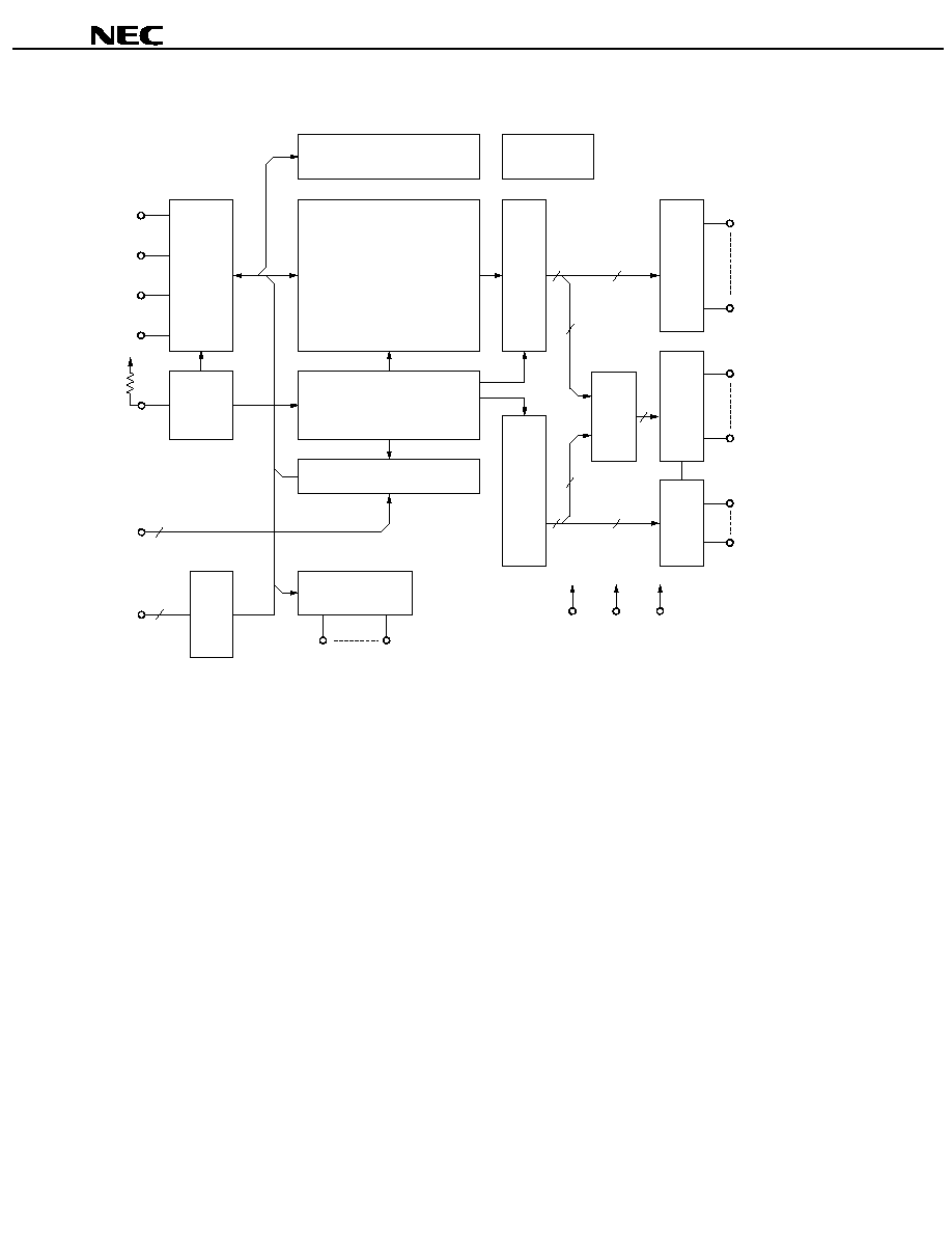
The
PD16311 is a FIP (Fluorescent Indicator Panel or Vacuum Fluorescent Display) controller/driver that is
driven on a 1/8- to 1/16 duty factor. It consists of 12 segment output lines, 8 grid output lines, 8 segment/grid output
drive lines, a display memory, a control circuit, and a key scan circuit. Serial data is input to the
PD16311 through a
three-line serial interface. This FIP controller/driver is ideal as a peripheral device of a single-chip microcomputer.
FEATURES
∑ Many display modes (12-segment & 16-digit to 20-segment & 8-digit)
∑ Key scanning (12
4 matrices)
∑ Dimming circuit (eight steps)
∑ High-voltage output (V
DD
35 V max).
∑ LED ports (5 chs., 20 mA max).
∑ General-purpose input port (4 bits)
∑ No external resistor necessary for driver outputs (P-ch open-drain + pull-down resistor output)
∑ Serial interface (CLK, STB, D
IN
, D
OUT
)
ORDERING INFORMATION
Part Number
Package
PD16311GC-AB6
52-pin plastic QFP ( 14)
2
PD16311
BLOCK DIAGRAM
D
IN
D
OUT
CLK
Key
1
to
Key
4
SW
1
to
SW
4
STB
R
4
4
OSC
5-bit latch
Key data memory (4
◊
12)
Timing generator
key scan
Display memory
20 bit
◊
16 Word
Command decoder
Dimming
circuit
4-bit latch
16
8
8
8
8
20
12
Seg
1
Seg
12
Seg
13
/Grid
16
Seg
20
/Grid
9
Grid
1
Grid
8
16-bit shift register
Data selector
Segment/grid
driver
Grid driver
Segment driver
20-bit output latch
Serial I/F
V
DD
LED
1
LED
5
V
DD
(+5 V)
V
SS
(0 V)
V
EE
(
-
30 V)

3
PD16311
PIN CONFIGURATION (Top View)
1
SW
1
2
SW
2
3
SW
3
4
SW
4
5
D
OUT
6
D
IN
7
IC
8
CLK
9
STB
10
KEY
1
11
KEY
2
12
KEY
3
13
KEY
4
39
Grid
6
38
Grid
7
37
Grid
8
36
Seg
20
/Grid
9
35
Seg
19
/Grid
10
34
V
EE
33
V
DD
32
Seg
18
/Grid
11
31
Seg
17
/Grid
12
30
Seg
16
/Grid
13
29
Seg
15
/Grid
14
28
Seg
14
/Grid
15
27
Seg
13
/Grid
16
14
V
DD
15
Seg
1
/KS
1
16
Seg
2
/KS
2
17
Seg
3
/KS
3
18
Seg
4
/KS
4
19
Seg
5
/KS
5
20
Seg
6
/KS
6
21
Seg
7
/KS
7
22
Seg
8
/KS
8
23
Seg
9
/KS
9
24
Seg
10
/KS
10
25
Seg
11
/KS
11
26
Seg
12
/KS
12
52
OSC
51
V
SS
50
LED
1
49
LED
2
48
LED
3
47
LED
4
46
LED
5
45
V
DD
44
Grid
1
43
Grid
2
42
Grid
3
41
Grid
4
40
Grid
5
Use all the power pins. Leave the IC pin open.

4
PD16311
Pin Function
Pin No.
Symbol
Pin Name
Description
6
D
IN
Data input
Inputs serial data at rising edge of shift clock, starting from lower
bit.
5
D
OUT
Data output
Outputs serial data at falling edge of shift clock, starting from
lower bit. This is N-ch open-drain output pin.
9
STB
Strobe
Initializes serial interface at rising or falling edge to make
PD16311 waiting for reception of command. Data input after
STB has fallen is processed as command. While command data
is processed, current processing is stopped, and serial interface
is initialized. While STB is high, CLK is ignored.
8
CLK
Clock input
Reads serial data at rising edge, and outputs data at falling edge.
52
OSC
Oscillator pin
Connect resistor for determining oscillation frequency to this pin.
15 to 26
Seg
1
/KS
1
to
Seg
12
/KS
12
High-voltage output
(segment)
Segment output pins (Dual function as key source)
44 to 37
Grid
1
to Grid
6
High-voltage output (grid)
Grid output pins
27 to 32
35 to 36
Seg
13
/Grid
16
to
Seg
20
/Grid
9
High-voltage output
(segment/grid)
These pins are selectable for segment or grid output.
50 to 46
LED
1
to LED
5
LED output
CMOS output. +20 mA max.
10 to 13
Key
1
to Key
4
Key data input
Data input to these pins is latched at end of display cycle.
1 to 4
SW
1
to SW
4
Switch input
These pins constitute 4-bit general-purpose input port.
14, 33, 45
V
DD
Logic power
5 V
10 %
51
V
SS
Logic ground
Connect this pin to GND of system.
34
V
EE
Pull-down level
V
DD
35 V max.
7
IC
Internally connected
Be sure to leave this pin open (this pin is at V
DD
level).
5
PD16311
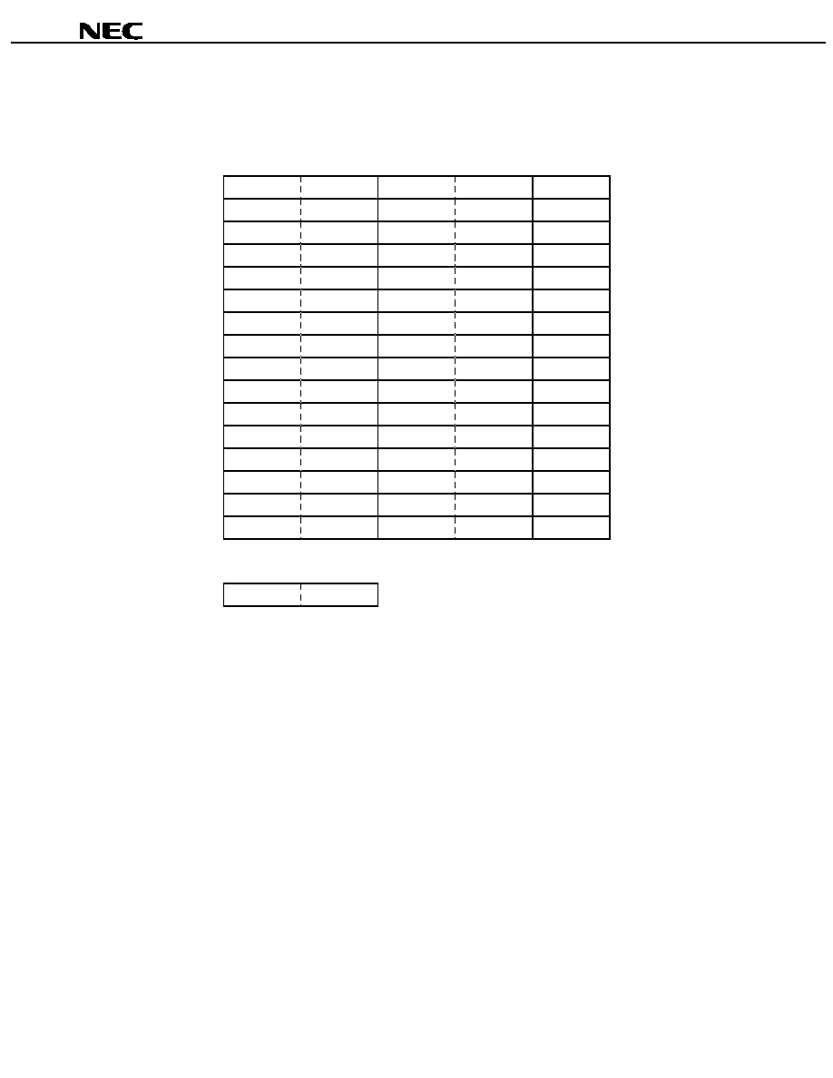
Display RAM Address and Display Mode
The display RAM stores the data transmitted from an external device to the
PD16311 through the serial interface,
and is assigned addresses as follows, in units of 8 bits:
Seg
1
Seg
4
Seg
8
Seg
12
Seg
16
Seg
20
00 H
L
00 H
U
01 H
L
01 H
U
02 H
L
DIG
1
03 H
L
03 H
U
04 H
L
04 H
U
05 H
L
DIG
2
06 H
L
06 H
U
07 H
L
07 H
U
08 H
L
DIG
3
09 H
L
09 H
U
0 AH
L
0 AH
U
0 BH
L
DIG
4
0 CH
L
0 CH
U
0 DH
L
0 DH
U
0 EH
L
DIG
5
0 FH
L
0 FH
U
10 H
L
10 H
U
11 H
L
DIG
6
12 H
L
12 H
U
13 H
L
13 H
U
14 H
L
DIG
7
15 H
L
15 H
U
16 H
L
16 H
U
17 H
L
DIG
8
18 H
L
18 H
U
19 H
L
19 H
U
1 AH
L
DIG
9
1 BH
L
1 BH
U
1 CH
L
1 CH
U
1 DH
L
DIG
10
1 EH
L
1 EH
U
1 FH
L
1 FH
U
20 H
L
DIG
11
21 H
L
21 H
U
22 H
L
22 H
U
23 H
L
DIG1
2
24 H
L
24 H
U
25 H
L
25 H
U
26 H
L
DIG
13
27 H
L
27 H
U
28 H
L
28 H
U
29 H
L
DIG
14
2 AH
L
2 AH
U
2 BH
L
2 BH
U
2 CH
L
DIG
15
2 DH
L
2 DH
U
2 EH
L
2 EH
U
2 FH
L
DIG
16
b
0
b
3
b
4
b
7
XX H
L
XX H
U
Lower 4 bits
Higher 4 bits
Only the lower 4 bits of the addresses assigned to Seg
17
through Seg
20
are valid, and the higher 4 bits are
ignored.