 | –≠–ª–µ–∫—Ç—Ä–æ–Ω–Ω—ã–π –∫–æ–º–ø–æ–Ω–µ–Ω—Ç: EA-C10 | –°–∫–∞—á–∞—Ç—å:  PDF PDF  ZIP ZIP |
NEC Electronics Inc.
EA-C10
2.5-Volt, 0.25-Micron (drawn)
CMOS Embedded Array
March 1997
Preliminary
A12503EU1V0DS00
EA-C10 Series Features
EA-C10 Series Benefits
∑
0.25 µm drawn (0.18 µm L-effective) CMOS process
Ultra-high density cell structure with high performance
∑
Advanced embedded array architecture
Fast TAT and high integration of embedded megafunctions
∑
Available gate counts from 206K to 7 million gates
Support for a wide range of high-complexity systems
∑
Optimized 2.5V architecture (operates down to 1.8V)
Highest speed at ultra-low power consumption
∑
Significant low power dissipation of 0.14 µW/MHz/gate
New application possibilities and new system solutions
∑
Ultra-high pin count using 40 µm pad pitch
Increased I/O density to achieve smaller die sizes
∑
Special power rail structure, multi-oxide process
Mixed 2.5V / true 3.3V I/O for full system compatibility
∑
Cell-based I/O structure including LVDS, HSTL, GTL+, PCI
Flexible adaptation to system requirements
∑
Embedding of analog macros including DACs, ADCs
Mixed-signal design options
∑
Advanced packages such as TapeBGA, Flip Chip+BGA
Cost-effective and state-of-the-art packaging
∑
NEC's OpenCAD
Æ
design environment
Flexible design flow for short design times
Applications
The EA-C10 family is ideal for applications where high
density is mandatory and a short time-to-market path is
required. For example, RAM-dominated designs can be
realized with reduced die size and a reasonable turnaround
time. EA-C10 is well-suited for designs that may require
rework, because the logic function portion of the design
uses gate array primitives created just by the final metal
masks. Typical applications include engineering
workstations, telecommunications systems, advanced
graphics and low power applications where very high
performance is required.
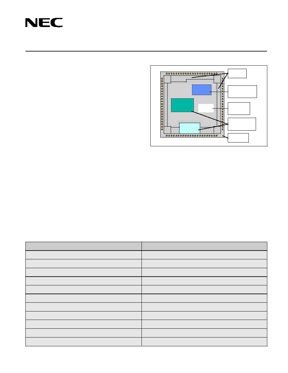
Figure 1. Embedded Array Core Integration
Table 1. EA-C10 Series Features and Benefits
Description
The high-speed 0.25 µm drawn (0.18 µm L-effective)
EA-C10 embedded array family offers both support for
embedded high-density macros as well as the short
turnaround time of a gate array resulting in a time-to-
market advantage. In this product, NEC combines high-
performance CMOS gate array primitives with diffused,
embedded megafunctions such as RAM, ROM, CPU,
DSP and analog cores.
EA-C10 also uses a cell-based I/O structure that allows a
flexible adaptation to the system requirements. State-of-
the-art interface macros for high-speed or special signaling
systems are also supported, such as PCI, HSTL, GTL+,
LVDS, p-ECL, and IEEE1394. Analog functions like DACs,
ADCs and PLLs also can be incorporated within the I/O
area.
Process
EA-C10 ASICs are manufactured with NEC's advanced
titanium-silicide (Ti-Si) process. The chip layout may use
between three and five metal layers (Al). As the EA-C10
ASIC family follows basically a gate array approach, it
offers short turnaround times for silicon processing and
lower development costs compared to cell-based ASICs.
The turnaround time is kept short by fixing the embedded
core locations and beginning prototype fabrication in
parallel with place and route design steps.
High Density
Memory
Analog
Macro
Logic
Function
Cell-Based
I/O Cells
High Density
Cell-Based
Compiled Memory
Gate Array
Primitives
(Sea-of-Gate)
Advanced Core
and
Analog Functions
Gate Array
Base Master
Core
or
Megafunction
OpenCAD is a registered trademark of NEC Electronics Inc.
All non-NEC trademarks are the property of their respective owners.

EA-C10
2
Interface Macro Support
The EA-C10 interface area uses the cell-based (CB-C10)
I/O structures that provide a variety of interface options,
including both 2.5-volt and 3.3-volt full-swing interface
buffers.
For special applications, several high-speed I/O buffer
types are available. These include 3.3-volt PCI cells, AGP
for 66 MHz and 133 MHz applications, GTL (Gunning
Transceiver Logic), HSTL (class 1,2,3,4) and pseudo-
ECL (pECL) buffers. These high-speed buffers are
available for special applications. Table 3 summarizes
the available interface options.
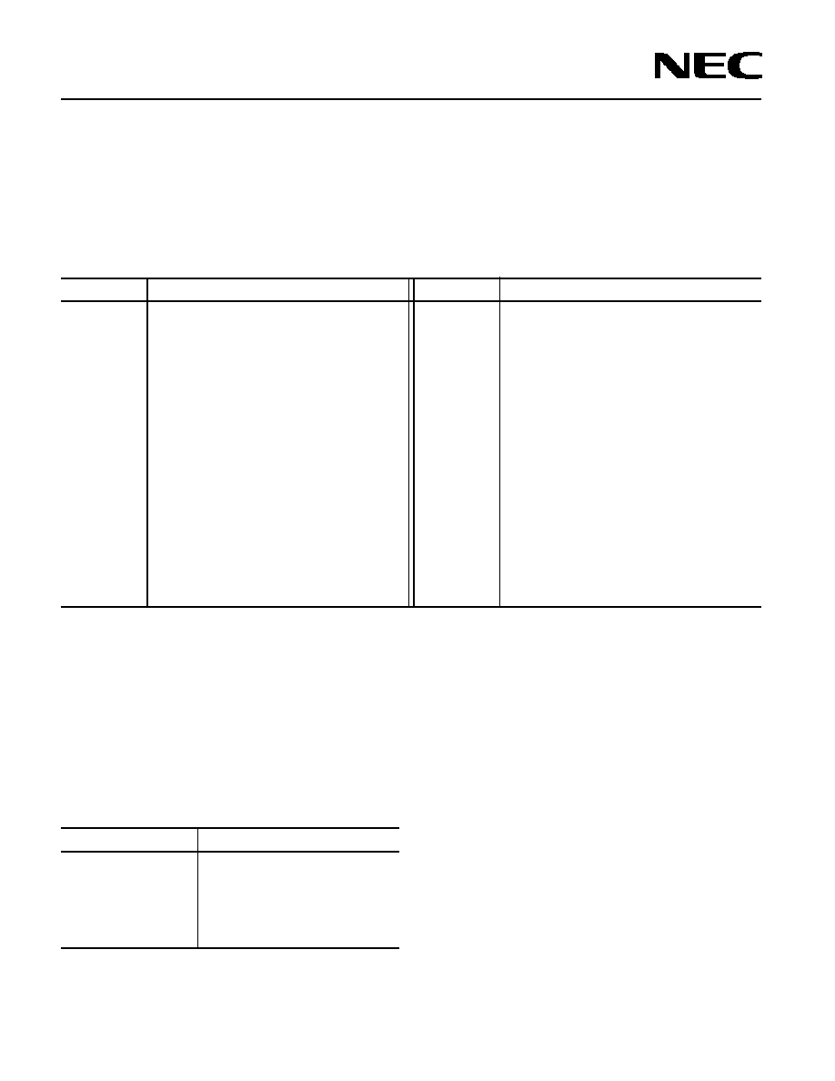
2.5-Volt / 3.3-Volt Mixed I/O Interfacing. Although
EA-C10 is a 2.5-volt optimized technology with thin gate
oxide, NEC offers 3.3-volt-compatible I/O interfacing.
The full-swing 3.3-volt interfacing is achieved through a
multi-oxide process in the I/O area. The buffers for 2.5-
volt / 3.3-volt interface levels can be mixed. This is
supported by the special power rail structure shown in
Figure 2.
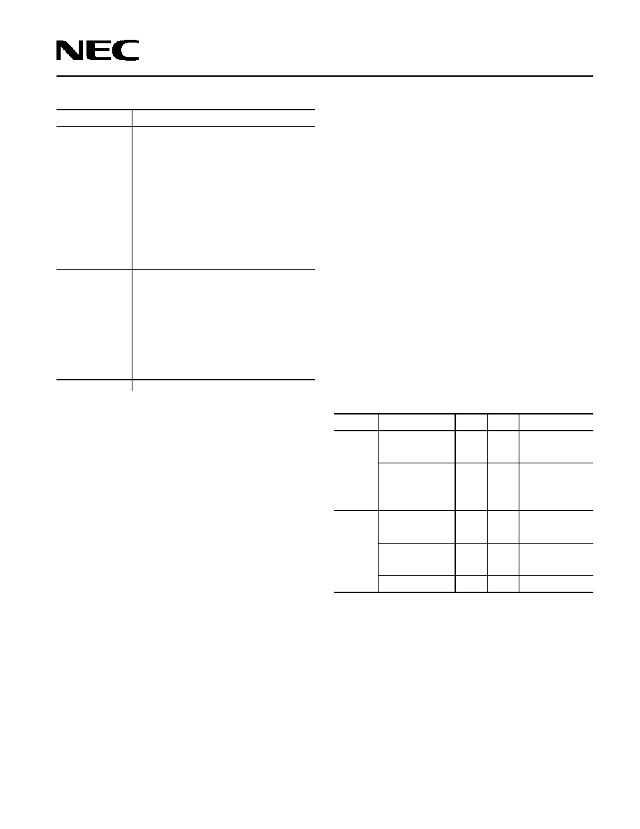
Table 2. Product Outline
Master (µPD69..) 3 layer
..101
..102
..103
..104
..105
..107
..109
..111
..112
..113
..114
..115
Master (µPD69..) 4 layer
..121
..122
..123
..124
..125
..127
..129
..131
..132
..133
..134
..135
Master (µPD69..) 5 layer*
..141
..142
..143
..144
..145
..147
..149
..151
..152
..153
..154
..155
Gate count (available)
206k
338k
497k
690k
1041k
1611k
2127k
2509k
3137k
3597k
4089k
6937k
Number of pads
(40 µm pitch)
348
444
540
636
780
972
1116
1212
1356
1452
1548
2016
Utilization
80% for 3-layer metal; 85% for 4-layer metal
Toggle frequency (typ.)
1.1 GHz
Internal
59 ps (F/O = 1, L = 0 mm); 147.5 ps (F/O = 2, L = typ. average length)
(F322 )
Delay time
Input
79.9 ps (F/O = 2, L = 0 mm)
(FI01)
Output
1.363 ns (C
L
= 50 pF)
(FO02)
Consumed
Internal
0.14
µ
W/MHz/gate (2.5V); 0.07
µ
W/MHz/gate (1.8V)
power
Input
1.66
µ
W/MHz (F/O = 2, L = 0 mm)
Output
167
µ
W/MHz (C
L
= 15 pF)
Power supply voltage
2.5 V
±
0.2V (operation down to 1.8V possible)
Operating temperature
-40 to +85∞C
Interface level
2.5V / 3.3V CMOS level, LVTTL level, GTL+,HSTL, PCI, pECL
Technology
Sea-of-gates 0.25
µ
m (drawn) silicon gate CMOS (0.18 L-effective), diffused embedded macros, 3, 4 or 5*
metal layers
Note: *5th metal layer used for flip-chip packaging
Figure 2. Power Rail Structure
Drawing not to scale
Internal Core
for internal power supply
V
DD
(2.5V, 3.3V)
V
DDQ
(ex. HSTL)
GND
increased internal
cell area
I/O area for 2.5V only
mixed voltage I/O area
2.5V I/O area
3.3V I/O area
V
D
D
Q
I
/
O
a
r
e
a
HSTL / PCI Interfacing. A third power rail (V
DDQ
) is
available for interface types that require a reference
voltage (such as HSTL, GTL+, and AGP). These buffers
may also be located anywhere in the I/O area.
3
EA-C10
Table 3. EA-C10 I/O Buffer Types
Buffer Type
Options and Possible Combinations
Standard I/O
Pull-up 50 k
, 5 k
/ Pull-down 50 k
Interface
Schmitt Trigger input
Buffers
Fail safe
LVCMOS / LVTTL level
Output buffers:
Open drain
Tri-state
Low noise (slew-rate controlled)
Driveability:
2.5V interface: 3, 6, 9, 12, 18, 24 mA/slot
3.3V interface: 3, 6, 9, 12, 24 mA/slot
High-Speed
PCI (3.3V, up to 64 bit / 66 MHz)
I/O Buffers
GTL / GTL+
pECL
HSTL
SSTL
LVDS*
AGP (66 MHz and 133 MHz)
IEEE1394*
USB*
Note: *Under development. Please check the availability of the
advanced interfaces with your nearest NEC design center.
Macro Library Support
The embedded array approach allows the combination of
high-density cores with a prototype turnaround time equal
to gate arrays. Megafunctions and memory blocks such
as RAM and ROM can be embedded into the sea-of-gates
area within the EA-C10 base master. The area used for
the megafunctions is defined by pre-diffusion. The logical
function is created by the final metalization masks. This
enables the usage of a gate array master and the whole
set of macros available in the cell-based technology CB-
C10. Cores from the BiCMOS family (QB-10) may also be
embedded.
Memory Macros. Various kinds of memory macros are
available for EA-C10. Designers can select either gate
array memory compilers using gate array cells or cell-
based compilers which offer higher density and faster
access times.
Cell-based type memory blocks are generated based on
advanced memory compiler tools and thus ensure highest
flexibility for design requirements. The available memory
types are described in Table 4.
Table 4. CMOS-10 / EA-C10 Memory Compilers
Family
Type
Mode Ports
Maximum Size
CMOS-10/
High-speed
Async.
1
8 Kbit
EA-C10
Aysnc.
2
8 Kbit
High-speed
Sync.
2
16 Kbit
Sync.
3
16 Kbit
Sync.
5
8 Kbit
EA-C10
High-density
Sync.
1
2K word x 32 bit
Sync.
2
2K word x 64 bit
High-speed
Sync.
1
2K word x 64 bit
Sync.
2
4K word x 64 bit
Super high-speed
Sync.
1
4K word x 64 bit
Block Library Support
EA-C10's functional blocks are designed to be backward-
compatible with previous families. Thus, an easy migration
from previous designs is possible. The library is fully
compatible with CMOS-10, the 0.25 µm (drawn) gate
array familiy.
The EA-C10 family offers a wide variety of advanced
blocks, including combinational gates, shift registers,
adders and counters. In addition, memory blocks such as
RAM and ROM are provided. The EA-C10 primitive
macros are available in up to four performance/power
options per primitive. With a range of options available,
popular design synthesis tools are able to make the
optimal size/performance/power choice for each path.
All memory macros can be combined with a built-in-self-
test (BIST) macro for easy and high-performance
production testing.
EA-C10
4
resolutions of 7 to 12 bits and a frequency of 100 kHz to
220 MHz for high-speed conversion.
Mega Macros. NEC offers a large set of megamacros
and cores to cope with today's system requirements.
Table 5 shows a subset of the macro portfolio.
Type
Description
Type
Description
Table 5. EA-C10 Mega Macro Library (subset listing)
CPU
V30MZTM: 16-bit microprocessor
CPU
V8xxTM: 32-bit RISC microcontroller
(several derivates)
CPU
ARM
CPU
VR4xxxTM: 64-bit RISC microcontroller
(several derivates)
Datapath
High-speed multiplier/accumulator
DSP
OAK: digital signal processor
DSP
PINE: digital signal processor
DSP
SPRX: digital signal processor
I/F peripheral
16550: UART with FIFO and 16450 mode
I/F peripheral
4993: 8-bit parallel I/O real-time clock
I/F peripheral
71037: DMA Controller
I/F peripheral
71051: USART, 300k bit/s, full-duplex
I/F peripheral
71054: programmable timer/counter
I/F peripheral
71055: programmable parallel interface (3x 8-bit)
I/F peripheral
71059: interrupt controller unit
I/F peripheral
ATM (25 MHz, 155 MHz)
I/F peripheral
CODEC (modem, voice)
I/F peripheral
Ethernet 10/100 base
I/F peripheral
IEEE 1284: bidirectional centronics
I/F peripheral
IEEE1394: high speed serial bus
I/F peripheral
MPEG2
I/F peripheral
PCI controller
I/F peripheral
RAC: RAMBUS ASIC Cell
I/F peripheral
USB: Universal Serial Bus interface
DPLL
Digital PLL (up to 250 MHz)
APLL
Analog PLL (up to 500 MHz)
Plastic BGAs with up to 672 balls can help to cope with
high-complexity system requirements by providing excel-
lent electrical and thermal characteristics. Tape BGA
packages support up to 1088 balls.
NEC expands the package offering continuously with new
advanced packages. For high-performance applications
with high pin counts, the 2-layer tape BGA with enhanced
electrical characteristics is available. Applications that
require ultra-dense packages can be realized with the flip-
chip package. This technique can also be used for Multi-
Chip Module (MCM) structures, where die mounting was
previously necessary.
Packaging
The advanced pad pitch of 40 µm allows high-pin-count
applications and gives a significant benefit for pad-limited
designs. EA-C10, the new high-performance embedded
array family, is supported by a variety of advanced pack-
ages. For lower pin counts (up to 376 pins), the standard
QFP is available, including the heat-spreader package
type to improve thermal characteristics.
Package Type
Maximum Pin/Ball Count
Plastic BGA
672
Tape BGA
1088
QFP
376 (0.4 mm pitch)
Flip-Chip
2016
Chip Scale
500
Analog Macros. A variety of A/D and D/A converters will
be available for analog applications. Analog-to-digital
converters (ADCs) are under development with a bit
resolution of 7 to 12 bits and a frequency of 100 kHz (for
general-purpose applications) up to 30 MHz. Digital-to-
analog converters (DACs) will also be developed with
V30MZ, V8xx, and Vr4xxx are trademarks of NEC Corporation.
5
EA-C10
CAD Support
NEC takes up the challenges of the new ultra-high-
density 0.25 µm technology by having close relationships
with leading EDA vendors to fulfill the design require-
ments during the whole design flow.
Fully supported by NEC's sophisticated OpenCAD
design
framework, EA-C10 maximizes design quality and flex-
ibility while minimizing ASIC design time.
NEC's OpenCAD
system allows designers to combine
the EDA industry's most popular third-party design tools
with proprietary NEC tools, including those for advanced
floorplanner, clock tree synthesis, automatic test pattern
generation (ATPG), full-timing simulation, accelerated
fault grading and advanced place and route algorithms.
The latest OpenCAD
system is open for sign-off using
standard EDA tools. NEC offers RTL- and STA-(Static
Timing Analysis) sign-off procedures to shorten the ASIC
design cycle of high-complexity designs.
Support of High-Speed Systems. High-speed systems
require tight control of clock skew on the chip and between
devices on a printed circuit board. CB-C10 provides two
features to control clock skew: the Digital PLL (DPLL)
working at frequencies up to 250 MHz for chip-to-chip
skew minimization and Clock Tree Synthesis (CTS).
CTS -- supported by an NEC proprietary design tool -- is
used for clock skew management through the automatic
insertion of a balanced buffer tree. The clock tree insertion
method minimizes large-capacitive trunks and is especially
useful with the hierarchical, synthesized design style
being used for high-integration devices. RC values for
actual net lengths of the clock tree are used for back
annotation after place and route operations. A skew as
low as ±60 ps can be achieved.
Accurate Design Verification.
Nonlinear timing
calculation is a very important requirement of the high-
density, deep sub-micron ASIC designs. NEC makes use
of the increased accuracy delivered by the nonlinear table
look-up delay calculation methodology and offers
consistent wire load models to ensure a high accuracy of
the design verification.
Design Rule Check. A comprehensive design rule
check (DRC) program reports design rule violations as
well as chip utilization statistics for the design netlist. The
generated report contains such information as net counts,
total pin and gate counts, and utilization figures.
Layout. During design synthesis, wire load models are
used to get delay estimations in a very early state of the
design flow. In general, there's no need for customers to
perform the floorplanning to meet the required timing.
During layout, enhanced in-place optimization (IPO)
features of the layout tools and engineering change order
(ECO) capabilities of the synthesis tools are used to
optimize critical timing paths defined by the given timing
constraints. This feature can reduce the total design time.
Test Support
The EA-C10 family supports automatic test generation
through a scan test methodology. It includes internal
scan, boundary scan (JTAG) and built-in-self-test (BIST)
architecture for easy and high-performance production
RAM testing. This allows higher fault coverage, easier
testing and faster development time.
Test of embedded megamacros is supported from NEC's
test bus concept, which allows the use of predefined test
pattern sets for integrated core macros.
Supplemental Publications
This data sheet contains preliminary specifications and
operational data for the EA-C10 embedded array family.
Additional information is available in NEC's EA-C10 Design
Manual, Block Library and other related documents.
Please refer also to the CMOS-10 and CB-C10 data
sheets to get more information about 0.25 µm gate array
and cell-based ASIC products.
Please contact your local NEC design center for additional
information; see the back of this data sheet for locations
and telephone numbers.