 | –≠–ª–µ–∫—Ç—Ä–æ–Ω–Ω—ã–π –∫–æ–º–ø–æ–Ω–µ–Ω—Ç: FB1J3P | –°–∫–∞—á–∞—Ç—å:  PDF PDF  ZIP ZIP |
1998
©
Document No. D16180EJ1V0DS00 (1st edition)
Date Published April 2002 N CP(K)
Printed in Japan
COMPOUND TRANSISTOR
FB1 SERIES
on-chip resistor NPN silicon epitaxial transistor
For mid-speed switching
DATA SHEET
2002
The information in this document is subject to change without notice. Before using this document, please
confirm that this is the latest version.
Not all devices/types available in every country. Please check with local NEC representative for
availability and additional information.
FEATURES
∑
Up to 0.7 A current drive available
∑
On-chip bias resistor
∑
Low power consumption during drive
QUALITY GRADES
∑
Standard
Please refer to "Quality Grades on NEC Semiconductor
Devices" (Document No. C11531E) published by NEC Corporation
to know the specification of quality grade on the devices and its
recommended applications.
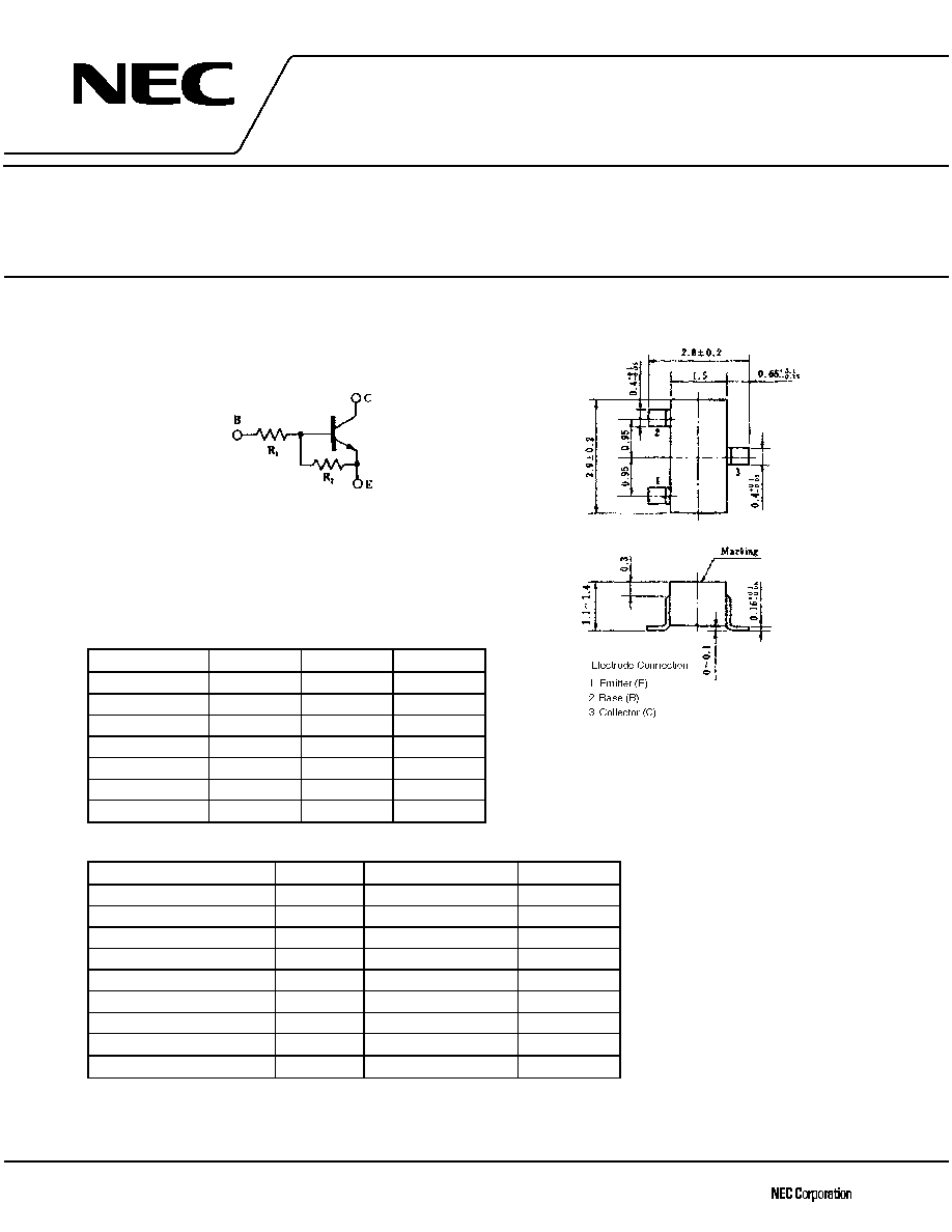
FB1 SERIES LISTS
Products
Marking
R
1
(K
)
R
2
(K
)
FB1A4A
P30
-
10
FB1L2Q
P31
0.47
4.7
FB1A3M
P32
1.0
1.0
FB1F3P
P33
2.2
10
FB1J3P
P36
3.3
10
FB1L3N
P34
4.7
10
FB1A4M
P35
10
10
PACKAGE DRAWING (UNIT: mm)
ABSOLUTE MAXIMUM RATINGS (Ta = 25
∞
∞
∞
∞C)
Parameter
Symbol
Ratings
Unit
Collector to base voltage
V
CBO
30
V
Collector to emitter voltage
V
CEO
25
V
Emitter to base voltage
V
EBO
10
V
Collector current (DC)
I
C(DC)
0.7
A
Collector current (Pulse)
I
C(pulse)
*
1.0
A
Base current (DC)
I
B(DC)
20
mA
Total power dissipation
P
T
200
mW
Junction temperature
T
j
150
∞C
Storage temperature
T
stg
-55 to +150
∞C
* PW
10 ms, duty cycle50 %
Data Sheet D16180EJ1V0DS
2
FB1 SERIES
FB1A4A
ELECTRICAL CHARACTERISTICS (Ta = 25
∞
∞
∞
∞C)
Parameter
Symbol
Conditions
MIN.
TYP.
MAX.
Unit
Collector cutoff current
I
CBO
V
CB
= 30 V, I
E
= 0
100
nA
DC current gain
h
FE1
**
V
CE
= 2.0 V, I
C
= 0.1 A
300
-
DC current gain
h
FE2
**
V
CE
= 2.0 V, I
C
= 0.5 A
300
-
DC current gain
h
FE3
**
V
CE
= 2.0 V, I
C
= 0.7 A
135
-
Collector saturation voltage
V
CE(sat)
**
I
C
= 0.5 A, I
B
= 5 mA
0.27
0.4
V
Low level input voltage
V
IL
**
V
CE
= 5.0 V, I
C
= 100
µA
0.3
V
Input resistance
R
1
-
-
-
E-to-B resistance
R
2
7
10
13
k
** PW
350
µs, duty cycle 2 %
FB1L2Q
ELECTRICAL CHARACTERISTICS (Ta = 25
∞
∞
∞
∞C)
Parameter
Symbol
Conditions
MIN.
TYP.
MAX.
Unit
Collector cutoff current
I
CBO
V
CB
= 30 V, I
E
= 0
100
nA
DC current gain
h
FE1
**
V
CE
= 2.0 V, I
C
= 0.1 A
150
400
-
DC current gain
h
FE2
**
V
CE
= 2.0 V, I
C
= 0.5 A
300
700
-
DC current gain
h
FE3
**
V
CE
= 2.0 V, I
C
= 0.7 A
135
600
-
Low level output voltage
V
OL
**
V
IN
= 5.0 V, I
C
= 0.5 A
0.2
0.3
V
Low level input voltage
V
IL
**
V
CE
= 5.0 V, I
C
= 100
µA
0.62
0.3
V
Input resistance
R
1
329
470
611
E-to-B resistance
R
2
3.29
4.7
6.11
k
** PW
350
µs, duty cycle 2 %
FB1A3M
ELECTRICAL CHARACTERISTICS (Ta = 25
∞
∞
∞
∞C)
Parameter
Symbol
Conditions
MIN.
TYP.
MAX.
Unit
Collector cutoff current
I
CBO
V
CB
= 30 V, I
E
= 0
100
nA
DC current gain
h
FE1
**
V
CE
= 2.0 V, I
C
= 0.1 A
80
-
DC current gain
h
FE2
**
V
CE
= 2.0 V, I
C
= 0.5 A
100
-
DC current gain
h
FE3
**
V
CE
= 2.0 V, I
C
= 0.7 A
135
-
Low level output voltage
V
OL
**
V
IN
= 5.0 V, I
C
= 0.5 A
0.3
0.4
V
Low level input voltage
V
IL
**
V
CE
= 5.0 V, I
C
= 100
µA
0.3
V
Input resistance
R
1
0.7
1.0
1.3
k
E-to-B resistance
R
2
0.7
1.0
1.3
k
** PW
350
µs, duty cycle 2 %
Data Sheet D16180EJ1V0DS
3
FB1 SERIES
FB1F3P
ELECTRICAL CHARACTERISTICS (Ta = 25
∞
∞
∞
∞C)
Parameter
Symbol
Conditions
MIN.
TYP.
MAX.
Unit
Collector cutoff current
I
CBO
V
CB
= 30 V, I
E
= 0
100
nA
DC current gain
h
FE1
**
V
CE
= 2.0 V, I
C
= 0.1 A
300
-
DC current gain
h
FE2
**
V
CE
= 2.0 V, I
C
= 0.5 A
300
-
DC current gain
h
FE3
**
V
CE
= 2.0 V, I
C
= 0.7 A
135
-
Low level output voltage
V
OL
**
V
IN
= 5.0 V, I
C
= 0.3 A
0.3
V
Low level input voltage
V
IL
**
V
CE
= 5.0 V, I
C
= 100
µA
0.3
V
Input resistance
R
1
1.54
2.2
2.86
k
E-to-B resistance
R
2
7
10
13
k
** PW
350
µs, duty cycle 2 %
FB1J3P
ELECTRICAL CHARACTERISTICS (Ta = 25
∞
∞
∞
∞C)
Parameter
Symbol
Conditions
MIN.
TYP.
MAX.
Unit
Collector cutoff current
I
CBO
V
CB
= 30 V, I
E
= 0
100
nA
DC current gain
h
FE1
**
V
CE
= 2.0 V, I
C
= 0.1 A
300
600
-
DC current gain
h
FE2
**
V
CE
= 2.0 V, I
C
= 0.5 A
300
700
-
DC current gain
h
FE3
**
V
CE
= 2.0 V, I
C
= 0.7 A
135
600
-
Low level output voltage
V
OL
**
V
IN
= 5.0 V, I
C
= 0.2 A
0.14
0.3
V
Low level input voltage
V
IL
**
V
CE
= 5.0 V, I
C
= 100
µA
0.6
0.3
V
Input resistance
R
1
2.31
3.3
4.29
k
E-to-B resistance
R
2
7
10
13
k
** PW
350
µs, duty cycle 2 %
FB1L3N
ELECTRICAL CHARACTERISTICS (Ta = 25
∞
∞
∞
∞C)
Parameter
Symbol
Conditions
MIN.
TYP.
MAX.
Unit
Collector cutoff current
I
CBO
V
CB
= 30 V, I
E
= 0
100
nA
DC current gain
h
FE1
**
V
CE
= 2.0 V, I
C
= 0.1 A
300
-
DC current gain
h
FE2
**
V
CE
= 2.0 V, I
C
= 0.5 A
300
-
DC current gain
h
FE3
**
V
CE
= 2.0 V, I
C
= 0.7 A
135
-
Low level output voltage
V
OL
**
V
IN
= 5.0 V, I
C
= 0.2 A
0.3
V
Low level input voltage
V
IL
**
V
CE
= 5.0 V, I
C
= 100
µA
0.3
V
Input resistance
R
1
3.29
4.7
6.11
k
E-to-B resistance
R
2
7
10
13
k
** PW
350
µs, duty cycle 2 %
Data Sheet D16180EJ1V0DS
4
FB1 SERIES
FB1A4M
ELECTRICAL CHARACTERISTICS (Ta = 25
∞
∞
∞
∞C)
Parameter
Symbol
Conditions
MIN.
TYP.
MAX.
Unit
Collector cutoff current
I
CBO
V
CB
= 30 V, I
E
= 0
100
nA
DC current gain
h
FE1
**
V
CE
= 2.0 V, I
C
= 0.1 A
300
-
DC current gain
h
FE2
**
V
CE
= 2.0 V, I
C
= 0.5 A
300
-
DC current gain
h
FE3
**
V
CE
= 2.0 V, I
C
= 0.7 A
135
-
Collector saturation voltage
V
CE(sat)
**
V
IN
= 5.0 V, I
C
= 0.2 A
0.3
V
Low level input voltage
V
IL
**
V
CE
= 5.0 V, I
C
= 100
µA
0.3
V
Input resistance
R
1
7
10
13
k
E-to-B resistance
R
2
7
10
13
k
** PW
350
µs, duty cycle 2 %
Data Sheet D16180EJ1V0DS
5
FB1 SERIES
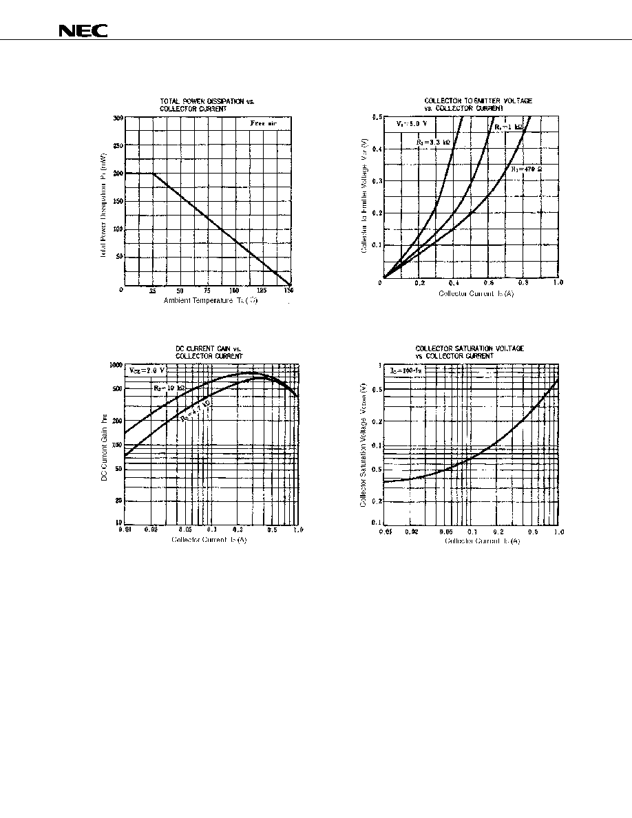
TYPICAL CHARACTERISTICS (T
a
= 25
∞
∞
∞
∞C)
Data Sheet D16180EJ1V0DS
6
FB1 SERIES
RECOMMENDED SOLDERING CONDITIONS
This product should be soldered and mounted under the following recommended conditions.
For soldering methods and conditions other than those recommended below, contact an NEC sales representative.
Surface MOUNTING TYPE
For details of the recommended soldering conditions, refer to the document Semiconductor Device Mounting
Technology Manual (C10535E).
Soldering Method
Soldering Conditions
Recommended
Condition Symbol
Infrared reflow
Package peak temperature: 230
∞C, Time: 30 sec. max. (at 210∞C or higher),
Count: Once, Exposure limit: None *
IR30-00
VPS
Package peak temperature: 215
∞C, Time: 40 sec. max. (at 200∞C or higher),
Count: Once, Exposure limit: None *
VP15-00
Partial heating
Pin temperature: 300
∞C max., Time: 10 sec. max. Exposure limit: None *
O
* After opening the dry pack, store it at 25
∞C or less and 65% RH or less for the allowable storage period.
Cautions 1. Do not use different soldering methods together (except for partial heating).
2. Prevent the resin surface temperature from being higher than the board temperature by 20
∞
∞
∞
∞C or
more.

Data Sheet D16180EJ1V0DS
7
FB1 SERIES
[MEMO]
FB1 SERIES
M8E 00. 4
The information in this document is current as of July, 2001. The information is subject to change
without notice. For actual design-in, refer to the latest publications of NEC's data sheets or data
books, etc., for the most up-to-date specifications of NEC semiconductor products. Not all products
and/or types are available in every country. Please check with an NEC sales representative for
availability and additional information.
No part of this document may be copied or reproduced in any form or by any means without prior
written consent of NEC. NEC assumes no responsibility for any errors that may appear in this document.
NEC does not assume any liability for infringement of patents, copyrights or other intellectual property rights of
third parties by or arising from the use of NEC semiconductor products listed in this document or any other
liability arising from the use of such products. No license, express, implied or otherwise, is granted under any
patents, copyrights or other intellectual property rights of NEC or others.
Descriptions of circuits, software and other related information in this document are provided for illustrative
purposes in semiconductor product operation and application examples. The incorporation of these
circuits, software and information in the design of customer's equipment shall be done under the full
responsibility of customer. NEC assumes no responsibility for any losses incurred by customers or third
parties arising from the use of these circuits, software and information.
While NEC endeavours to enhance the quality, reliability and safety of NEC semiconductor products, customers
agree and acknowledge that the possibility of defects thereof cannot be eliminated entirely. To minimize
risks of damage to property or injury (including death) to persons arising from defects in NEC
semiconductor products, customers must incorporate sufficient safety measures in their design, such as
redundancy, fire-containment, and anti-failure features.
NEC semiconductor products are classified into the following three quality grades:
"Standard", "Special" and "Specific". The "Specific" quality grade applies only to semiconductor products
developed based on a customer-designated "quality assurance program" for a specific application. The
recommended applications of a semiconductor product depend on its quality grade, as indicated below.
Customers must check the quality grade of each semiconductor product before using it in a particular
application.
"Standard": Computers, office equipment, communications equipment, test and measurement equipment, audio
and visual equipment, home electronic appliances, machine tools, personal electronic equipment
and industrial robots
"Special":
Transportation equipment (automobiles, trains, ships, etc.), traffic control systems, anti-disaster
systems, anti-crime systems, safety equipment and medical equipment (not specifically designed
for life support)
"Specific": Aircraft, aerospace equipment, submersible repeaters, nuclear reactor control systems, life
support systems and medical equipment for life support, etc.
The quality grade of NEC semiconductor products is "Standard" unless otherwise expressly specified in NEC's
data sheets or data books, etc. If customers wish to use NEC semiconductor products in applications not
intended by NEC, they must contact an NEC sales representative in advance to determine NEC's willingness
to support a given application.
(Note)
(1) "NEC" as used in this statement means NEC Corporation and also includes its majority-owned subsidiaries.
(2) "NEC semiconductor products" means any semiconductor product developed or manufactured by or for
NEC (as defined above).
∑
∑
∑
∑
∑
∑