
©
1994,1996
DATA SHEET
MOS INTEGRATED CIRCUIT
Description
The
µ
PD485505 is a 5,048 words by 8 bits high speed FIFO (First In First Out) line buffer. Its CMOS static circuitry
provides high speed access and low power consumption.
The
µ
PD485505 can be used for one line delay and time axis conversion in high speed facsimile machines and
digital copiers.
Moreover, the
µ
PD485505 can execute read and write operations independently on an asynchronous basis. Thus
the
µ
PD485505 is suitable as a buffer for data transfer between units with different transfer rates and as a buffer for
the synchronization of multiple input signals. There are three versions, E, K, P, and L. This data sheet can be applied
to the version P and L. These versions operate with different specifications. Each version is identified with its lot
number (refer to 7. Example of Stamping).
Features
∑
5,048 words by 8 bits
∑
Asynchronous read/write operations available
∑
Variable length delay bits; 21 to 5,048 bits (Cycle time: 25 ns)
15 to 5,048 bits (Cycle time: 35 ns)
∑
Power supply voltage V
CC
= 5.0 V
±
0.5 V
∑
Suitable for sampling one line of A3 size paper (16 dots/mm)
∑
All input/output TTL compatible
∑
3-state output
∑
Full static operation; data hold time = infinity
Ordering Information
Part Number
R/W Cycle Time
Package
µ
PD485505G-25
25 ns
24-pin plastic SOP
µ
PD485505G-35
35 ns
(11.43 mm (450))
µ
PD485505
LINE BUFFER
5K-WORD BY 8-BIT
The mark shows major revised points.
Document No. M10059EJ7V0DSJ1 (7th edition)
Date Published December 2000 N CP(K)
Printed in Japan
The information in this document is subject to change without notice. Before using this document, please
confirm that this is the latest version.
Not all devices/types available in every country. Please check with local NEC representative for availability
and additional information.

µ
PD485505
2
Data Sheet M10059EJ7V0DS00
Pin Configuration (Marking side)
24-pin plastic SOP (11.43 mm (450))
[
µ
PD485505G]
D
OUT0
D
OUT1
D
OUT2
D
OUT3
RE
RSTR
GND
RCK
D
OUT4
D
OUT5
D
OUT6
D
OUT7
1
2
3
4
5
6
7
8
9
10
11
12
24
23
22
21
20
19
18
17
16
15
14
13
D
IN0
D
IN1
D
IN2
D
IN3
WE
RSTW
V
CC
WCK
D
IN4
D
IN5
D
IN6
D
IN7
D
IN0
- D
IN7
: Data Inputs
D
OUT0
- D
OUT7
: Data Outputs
WCK
: Write Clock Input
RCK
: Read Clock Input
WE
: Write Enable Input
RE
: Read Enable Input
RSTW
: Reset Write Input
RSTR
: Reset Read Input
V
CC
: +5.0 V Power Supply
GND
: Ground
Remark
Refer to 5. Package Drawing for the 1-pin index mark.
µ
PD485505
3
Data Sheet M10059EJ7V0DS00
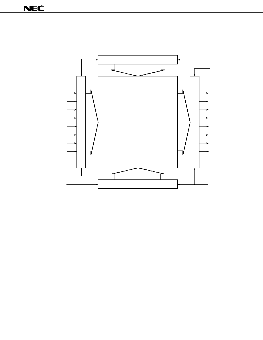
Block Diagram
D
IN0
D
IN1
D
IN2
D
IN3
D
IN4
D
IN5
D
IN6
D
IN7
WE
RSTR
WCK
D
OUT0
D
OUT1
D
OUT2
D
OUT3
D
OUT4
D
OUT5
D
OUT6
D
OUT7
RCK
RSTW
RE
V
CC
GND
Write Address Pointer
Read Address Pointer
Input Buffer
Output Buffer
Memory Cell Array
40,384 bits
(5,048 words by 8 bits)

µ
PD485505
4
Data Sheet M10059EJ7V0DS00
1. Input/Output Pin Function
Pin
Pin
Symbol
Pin
Number
Name
24 - 21
D
IN0
Data
|
Input
16 - 13
D
IN7
1 - 4
D
OUT0
Data
|
Output
9 - 12
D
OUT7
19
RSTW
Reset
Write
Input
6
RSTR
Reset
Read
Input
20
WE
Write
Enable
Input
5
RE
Read
Enable
Input
17
WCK
Write
Clock
Input
8
RCK
Read
Clock
Input
I/O
Function
In
Write data input pins.
The data inputs are strobed by the rising edge of WCK at the end of a cycle
and the setup and hold times (t
DS
, t
DH
) are defined at this point.
Out
Read data output pins.
The access time is regulated from the rising edge of RCK at the beginning of a
cycle and defined by t
AC
.
In
Reset input pin for the initialization of the write address pointer.
The state of RSTW is strobed by the rising edge of WCK at the beginning of a
cycle and the setup and hold times (t
RS
, t
RH
) are defined.
In
Reset input pin for the initialization of the read address pointer.
The state of RSTR is strobed by the rising edge of RCK at the beginning of a
cycle and the setup and hold times (t
RS
, t
RH
) are defined.
In
Write operation control signal input pin.
When WE is in the disable mode ("H" level), the internal write operation is
inhibited and the write address pointer stops at the current position.
In
Read operation control signal input pin.
When RE is in the disable mode ("H" level), the internal read operation is
inhibited and the read address pointer stops at the current position. The output
changes to high impedance.
In
Write clock input pin.
When WE is enabled ("L" level), the write operation is executed in
synchronization with the write clock. The write address pointer is incremented
simultaneously.
In
Read clock input pin.
When RE is enabled ("L" level), the read operation is executed in synchroniza-
tion with the read clock. The read address pointer is incremented
simultaneously.

µ
PD485505
5
Data Sheet M10059EJ7V0DS00
2. Operation Mode
µ
PD485505 is a synchronous memory. All signals are strobed at the rising edge of the clock (RCK, WCK).
For this reason, setup time and hold time are specified for the rising edge of the clock (RCK, WCK).
2.1 Write Cycle
When the WE input is enabled ("L" level), a write cycle is executed in synchronization with the WCK clock
input.
The data inputs are strobed by the rising edge of the clock at the end of a cycle so that read data after a one-
line (5,048 bits) delay and write data can be processed with the same clock. Refer to Write Cycle Timing Chart.
When WE is disabled ("H" level) in a write cycle, the write operation is not performed during the cycle which
the WCK rising edge is in the WE = "H" level (t
WEW
). The WCK does not increment the write address pointer
at this time.
Unless inhibited by WE, the internal write address will automatically wrap around from 5,047 to 0 and begin
incrementing again.
2.2 Read Cycle
When the RE input is enabled ("L" level), a read cycle is executed in synchronization with the RCK clock input
and data is output after t
AC
. Refer to Read Cycle Timing Chart.
When RE is disabled ("H" level) in a read cycle, the read operation is not performed during the cycle which
the RCK rising edge is in the RE = "H" level (t
REW
). The RCK does not increment the read address pointer at
this time.
2.3 Write Reset Cycle/Read Reset Cycle
After power up, the
µ
PD485505 requires the initialization of internal circuits because the read and write
address pointers are not defined at that time.
It is necessary to satisfy setup requirements and hold times as measured from the rising edge of WCK and
RCK, and then input the RSTW and RSTR signals to initialize the circuit.
Write and read reset cycles can be executed at any time and the address pointer returns zero. Refer to Write
Reset Cycle Timing Chart, Read Reset Cycle Timing Chart.
Remark
Write and read reset cycles can be executed at any time and do not depend on the state of RE or WE.