The information in this document is subject to change without notice. Before using this document, please
confirm that this is the latest version.
Not all devices/types available in every country. Please check with local NEC representative for
availability and additional information.
©
1995
MOS INTEGRATED CIRCUIT
µ
PD43256B-X
256K-BIT CMOS STATIC RAM
32K-WORD BY 8-BIT
EXTENDED TEMPERATURE OPERATION
DATA SHEET
Document No. M11012EJ4V0DSJ1 (4th edition)
Date Published December 2000 NS CP (K)
Printed in Japan
The mark
5
shows major revised points.
Description
The
µ
PD43256B-X is a high speed, low power, and 262,144 bits (32,768 words by 8 bits) CMOS static RAM.
The
µ
PD43256B-X is an extended-operating-temperature version of the
µ
PD43256B (X version : T
A
= ≠25 to +85
∞
C). And A and B versions are low voltage operations. Battery backup is available.
The
µ
PD43256B-X is packed in 28-pin plastic TSOP (I) (8 x 13.4 mm).
Features
∑
32,768 words by 8 bits organization
∑
Fast access time: 70, 85, 100, 120, 150 ns (MAX.)
∑
Operating ambient temperature: T
A
= ≠25 to +85
∞
C
∑
Low voltage operation (A version: V
CC
= 3.0 to 5.5 V, B version: V
CC
= 2.7 to 5.5 V)
∑
Low V
CC
data retention: 2.0 V (MIN.)
∑
/OE input for easy application
Part number
Access time
Operating supply Operating ambient
Supply current
ns (MAX.)
voltage
temperature
At operating
At standby
At data retention
V
∞C
mA (MAX.)
µ
A (MAX.)
µ
A (MAX.)
Note1
µ
PD43256B-xxX
70, 85
4.5 to 5.5
-
25 to +85
45
50
2
µ
PD43256B-AxxX
85
Note2
, 100, 120
Note2
3.0 to 5.5
µ
PD43256B-BxxX
Note2
100, 120
Note2
, 150
Note2
2.7 to 5.5
40
Notes 1. T
A
40
∞
C, V
CC
= 3.0 V
2. 100 s (MAX.) (V
CC
= 4.5 to 5.5 V)
Version X
This Data sheet can be applied to the version X. Each version is identified with its lot number. Letter X in the fifth
character position in a lot number signifies version X.
D43256B-X
Lot number
JAPAN
∑
3
µ
PD43256B-X
Data Sheet M11012EJ4V0DS
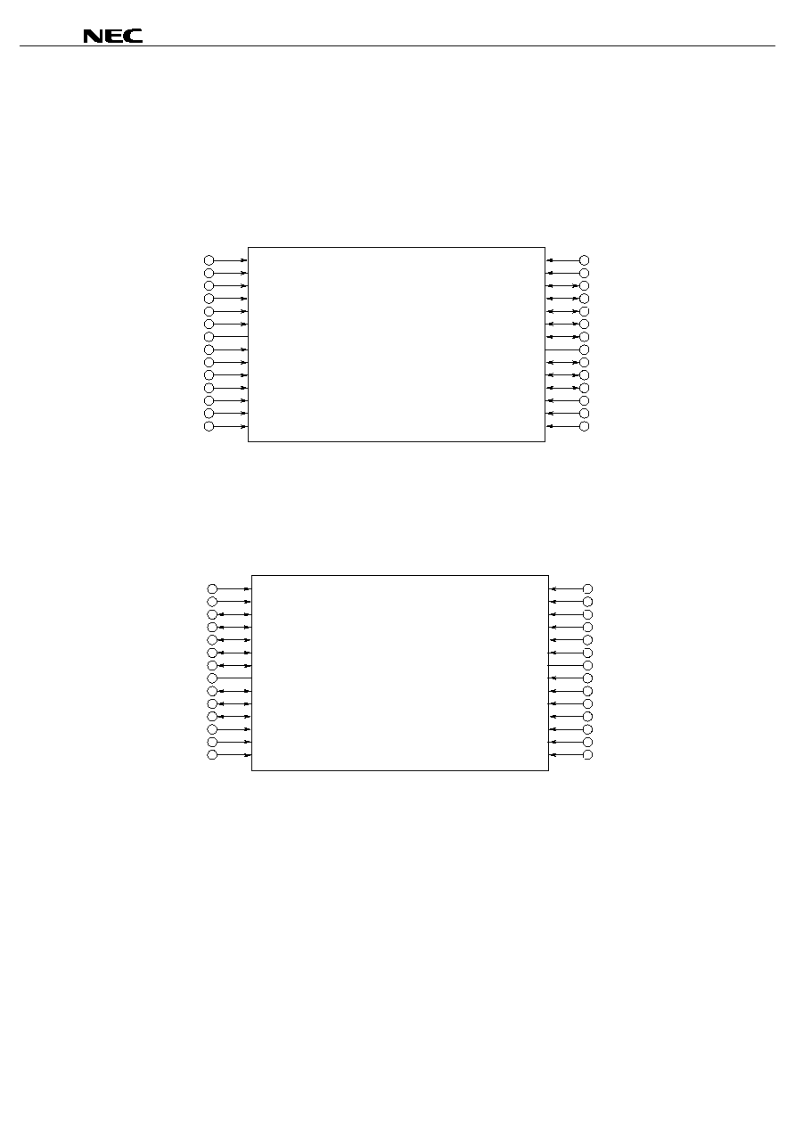
Pin Configurations (Marking Side)
/xxx indicates active low signal.
28-PIN PLASTIC TSOP(I) (8x13.4) (Normal bent)
[
µ
µ
µ
µ
PD43256BGW-xxX-9JL]
[
µ
µ
µ
µ
PD43256BGW-AxxX-9JL]
[
µ
µ
µ
µ
PD43256BGW-BxxX-9JL]
/OE
A11
A9
A8
A13
/WE
V
CC
A14
A12
A7
A6
A5
A4
A3
A10
/CS
I/O8
I/O7
I/O6
I/O5
I/O4
GND
I/O3
I/O2
I/O1
A0
A1
A2
1
2
3
4
5
6
7
8
9
10
11
12
13
14
28
27
26
25
24
23
22
21
20
19
18
17
16
15
28-PIN PLASTIC TSOP(I) (8x13.4) (Reverse bent)
[
µ
µ
µ
µ
PD43256BGW-xxX-9KL]
[
µ
µ
µ
µ
PD43256BGW-AxxX-9KL]
[
µ
µ
µ
µ
PD43256BGW-BxxX-9KL]
/OE
A11
A9
A8
A13
/WE
V
CC
A14
A12
A7
A6
A5
A4
A3
A10
/CS
I/O8
I/O7
I/O6
I/O5
I/O4
GND
I/O3
I/O2
I/O1
A0
A1
A2
1
2
3
4
5
6
7
8
9
10
11
12
13
14
28
27
26
25
24
23
22
21
20
19
18
17
16
15
A0 - A14
: Address inputs
I/O1 - I/O8
: Data inputs / outputs
/CS
: Chip Select
/WE
: Write Enable
/OE
: Output Enable
V
CC
: Power supply
GND
: Ground
Remark Refer to Package Drawings for the 1-pin index mark.
∑

5
µ
PD43256B-X
Data Sheet M11012EJ4V0DS
Electrical Specifications
Absolute Maximum Ratings
Parameter
Symbol
Condition
Rating
Unit
Supply voltage
V
CC
≠0.5
Note
to +7.0
V
Input / Output voltage
V
T
≠0.5
Note
to V
CC
+ 0.5
V
Operating ambient temperature
T
A
≠25 to +85
∞
C
Storage temperature
T
stg
≠55 to +125
∞
C
Note ≠3.0 V (MIN.) (Pulse width : 50 ns)
Caution
Exposing the device to stress above those listed in Absolute Maximum Rating could cause
permanent damage. The device is not meant to be operated under conditions outside the limits
described in the operational section of this specification. Exposure to Absolute Maximum Rating
conditions for extended periods may affect device reliability.
Recommended Operating Conditions
Parameter
Symbol Condition
µ
PD43256B-xxX
µ
PD43256B-AxxX
µ
PD43256B-BxxX
Unit
MIN.
MAX.
MIN.
MAX.
MIN.
MAX.
Supply voltage
V
CC
4.5
5.5
3.0
5.5
2.7
5.5
V
High level input voltage
V
IH
2.4
V
CC
+0.5
2.4
V
CC
+0.5
2.4
V
CC
+0.5
V
Low level input voltage
V
IL
≠0.3
Note
+0.6
≠0.3
Note
+0.4
≠0.3
Note
+0.4
V
Operating ambient temperature
T
A
≠25
+85
≠25
+85
≠25
+85
∞
C
Note ≠3.0 V (MIN.) (Pulse width: 50 ns)
Capacitance (T
A
= 25
∞
∞
∞
∞
C, f = 1 MHz)
Parameter
Symbol
Test conditions
MIN.
TYP.
MAX.
Unit
Input capacitance
C
IN
V
IN
= 0 V
5
pF
Input / Output capacitance
C
I/O
V
I/O
= 0 V
8
pF
Remarks 1. V
IN
: Input voltage
V
I/O
: Input / Output voltage
2. These parameters are periodically sampled and not 100% tested.