Document Outline
- COVER
- Features
- Ordering Information
- Pin Configuration
- Block Diagram
- Electrical Specifications
- Package Drawing
The information in this document is subject to change without notice. Before using this document, please
confirm that this is the latest version.
Not all products and/or types are available in every country. Please check with an NEC Electronics
sales representative for availability and additional information.
MOS INTEGRATED CIRCUIT
µ
µ
µ
µ
PD434016A
4M-BIT CMOS FAST SRAM
256K-WORD BY 16-BIT
DATA SHEET
Document No. M12228EJ8V0DS00 (8th edition)
Date Published December 2002 NS CP(K)
Printed in Japan
1996
Description
The
µPD434016A is a high speed, low power, 4,194,304 bits (262,144 words by 16 bits) CMOS static RAM.
Operating supply voltage is 5.0 V
± 0.5 V.
The
µPD434016A is packaged in 44-pin plastic SOJ and 44-pin plastic TSOP (II).
Features
∑ 262,144 words by 16 bits organization
∑ Fast access time : 12, 15, 17, 20 ns (MAX.)
∑ Byte data control : /LB (I/O1 to I/O8), /UB (I/O9 to I/O16)
∑ Output Enable input for easy application
∑ Single +5.0 V power supply
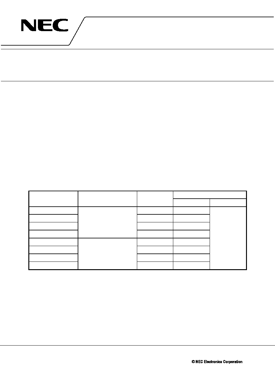
Ordering Information
Part number
Package
Access time
Supply current mA (MAX.)
ns (MAX.)
At operating
At standby
µPD434016ALE-12
44-pin plastic SOJ
12
230
10
µPD434016ALE-15
(10.16 mm (400))
15
200
µPD434016ALE-17
17
190
µPD434016ALE-20
20
180
µPD434016AG5-12-7JF
44-pin plastic TSOP (II)
12
230
µPD434016AG5-15-7JF
(10.16 mm (400))
15
200
µPD434016AG5-17-7JF
(Normal bent)
17
190
µPD434016AG5-20-7JF
20
180
2
µ
µ
µ
µPD434016A
Data Sheet M12228EJ8V0DS
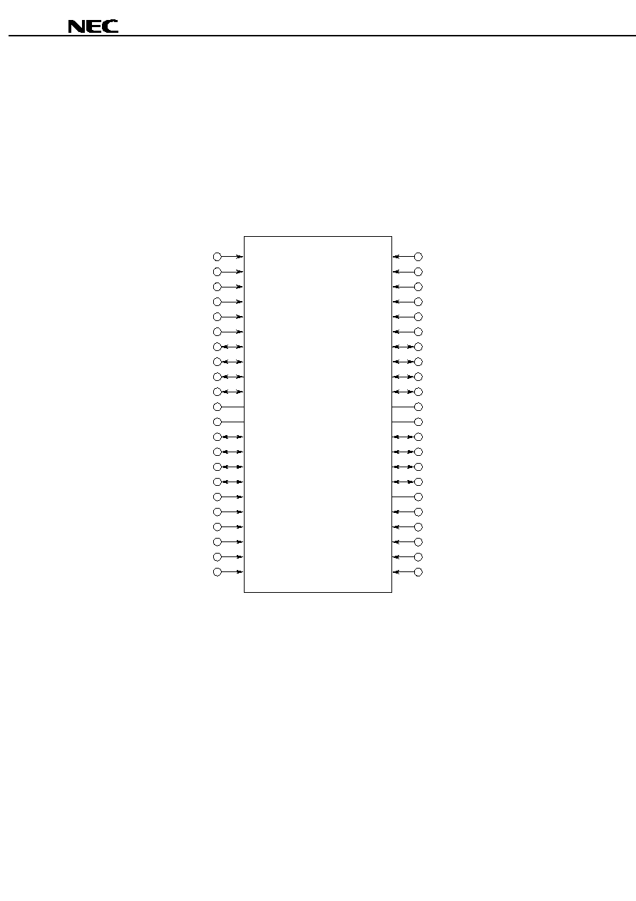
Pin Configuration
/xxx indicates active low signal.
44-pin plastic SOJ (10.16 mm (400))
[
µ
µ
µ
µPD434016ALE ]
44-pin plastic TSOP (II) (10.16 mm (400)) (Normal bent)
[
µ
µ
µ
µPD434016AG5-7JF ]
Marking Side
1
2
3
4
5
6
7
8
9
10
11
12
13
14
15
16
17
18
19
20
21
22
A0
A1
A2
A3
A4
/CS
I/O1
I/O2
I/O3
I/O4
V
CC
GND
I/O5
I/O6
I/O7
I/O8
/WE
A5
A6
A7
A8
A9
44
43
42
41
40
39
38
37
36
35
34
33
32
31
30
29
28
27
26
25
24
23
A17
A16
A15
/OE
/UB
/LB
I/O16
I/O15
I/O14
I/O13
GND
V
CC
I/O12
I/O11
I/O10
I/O9
NC
A14
A13
A12
A11
A10
A0 to A17
: Address Inputs
I/O1 to I/O16 : Data Inputs / Outputs
/CS
: Chip Select
/WE
: Write Enable
/OE
: Output Enable
/LB, /UB
: Byte data select
V
CC
: Power supply
GND
: Ground
NC
: No connection
Remark Refer to Package Drawings for the 1-pin index mark.
3
µ
µ
µ
µPD434016A
Data Sheet M12228EJ8V0DS
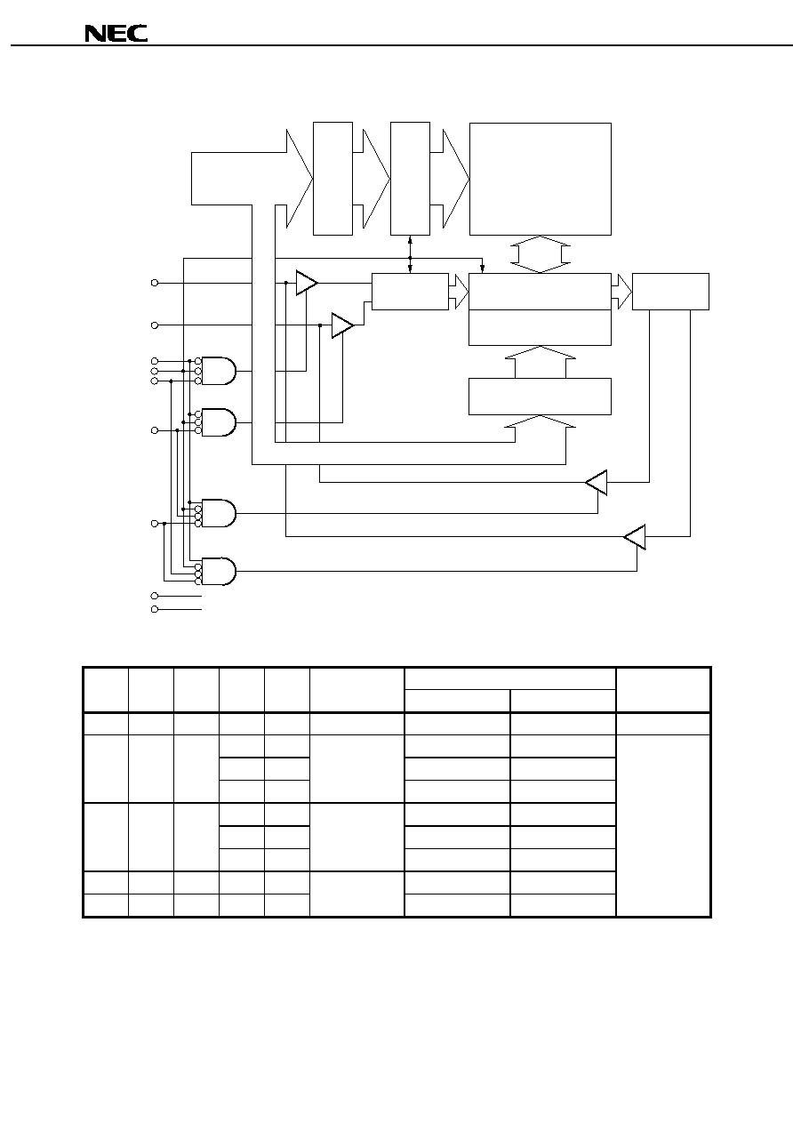
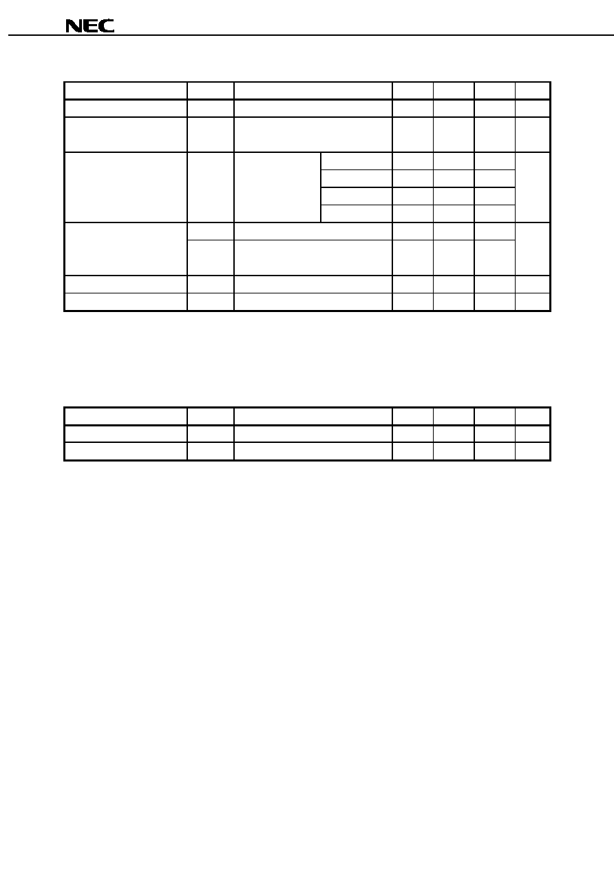
Block Diagram
GND
V
CC
/WE
/OE
/CS
Input data
controller
Sense amplifier /
Switching circuit
Column decoder
Address buffer
A0
|
A17
Address buffer
Row decoder
Memory cell array
4,194,304 bits
Output data
controller
/LB
/UB
I/O9 to I/O16
I/O1 to I/O8
Truth Table
/CS
/OE
/WE
/LB
/UB
Mode
I/O
Supply current
I/O1 to I/O8
I/O9 to I/O16
H
◊
◊
◊
◊
Not selected
High-Z
High-Z
I
SB
L
L
H
L
L
Read
D
OUT
D
OUT
I
CC
L
H
D
OUT
High-Z
H
L
High-Z
D
OUT
L
◊
L
L
L
Write
D
IN
D
IN
L
H
D
IN
High-Z
H
L
High-Z
D
IN
L
H
H
◊
◊
Output disable
High-Z
High-Z
L
◊
◊
H
H
High-Z
High-Z
Remark
◊ : Don't care
4
µ
µ
µ
µPD434016A
Data Sheet M12228EJ8V0DS
Electrical Specifications
Absolute Maximum Ratings
Parameter
Symbol
Condition
Rating
Unit
Supply voltage
V
CC
≠0.5
Note
to +7.0
V
Input / Output voltage
V
T
≠0.5
Note
to V
CC
+0.5
V
Operating ambient temperature
T
A
0 to 70
∞C
Storage temperature
T
stg
≠55 to +125
∞C
Note ≠2.0 V (MIN.) (pulse width : 2 ns)
Caution Exposing the device to stress above those listed in Absolute Maximum Rating could cause
permanent damage. The device is not meant to be operated under conditions outside the limits
described in the operational section of this specification. Exposure to Absolute Maximum Rating
conditions for extended periods may affect device reliability.
Recommended Operating Conditions
Parameter
Symbol
Condition
MIN.
TYP.
MAX.
Unit
Supply voltage
V
CC
4.5
5.0
5.5
V
High level input voltage
V
IH
2.2
V
CC
+0.5
V
Low level input voltage
V
IL
≠0.5
Note
+0.8
V
Operating ambient temperature
T
A
0
70
∞C
Note ≠2.0 V (MIN.) (pulse width : 2 ns)
5
µ
µ
µ
µPD434016A
Data Sheet M12228EJ8V0DS
DC Characteristics (Recommended Operating Conditions Unless Otherwise Noted)
Parameter
Symbol
Test condition
MIN.
TYP.
MAX.
Unit
Input leakage current
I
LI
V
IN
= 0 V to V
CC
≠2
+2
µA
Output leakage current
I
LO
V
I/O
= 0 V to V
CC
, /CS = V
IH
or /OE = V
IH
≠2
+2
µA
or /WE = V
IL
or /LB = V
IH
or /UB = V
IH
Operating supply current
I
CC
/CS = V
IL
,
Cycle time : 12 ns
230
mA
I
I/O
= 0 mA,
Cycle time : 15 ns
200
Minimum cycle time
Cycle time : 17 ns
190
Cycle time : 20 ns
180
Standby supply current
I
SB
/CS = V
IH
, V
IN
= V
IH
or V
IL
50
mA
I
SB1
/CS
V
CC
≠ 0.2 V,
10
V
IN
0.2 V or V
IN
V
CC
≠ 0.2 V
High level output voltage
V
OH
I
OH
= ≠4.0 mA
2.4
V
Low level output voltage
V
OL
I
OL
= +8.0 mA
0.4
V
Remarks 1. V
IN
: Input voltage
V
I/O
: Input / Output voltage
2. These DC characteristics are in common regardless of package types.
Capacitance (T
A
=
25
∞
∞
∞
∞C, f = 1 MHz)
Parameter
Symbol
Test condition
MIN.
TYP.
MAX.
Unit
Input capacitance
C
IN
V
IN
= 0 V
6
pF
Input / Output capacitance
C
I/O
V
I/O
= 0 V
10
pF
Remarks 1. V
IN
: Input voltage
V
I/O
: Input / Output voltage
2. These parameters are periodically sampled and not 100% tested.