The information in this document is subject to change without notice. Before using this document, please
confirm that this is the latest version.
Not all devices/types available in every country. Please check with local NEC representative for
availability and additional information.
©
1999
MOS INTEGRATED CIRCUIT
µ
µ
µ
µ
PD464518AL, 464536AL
4M-BIT Bi-CMOS SYNCHRONOUS FAST STATIC RAM
256K-WORD BY 18-BIT / 128K-WORD BY 36-BIT
LVTTL INTERFACE/REGISTER-LATCH/LATE WRITE
DATA SHEET
Document No. M13609EJ4V0DS00 (4th edition)
Date Published January 2001 NS CP(K)
Printed in Japan
The mark
∑
∑
∑
∑
shows major revised points.
Description
The
µ
PD464518AL is a 262,144 words by 18 bits, and the
µ
PD464536AL is a 131,072 words by 36 bits
synchronous static RAM fabricated with advanced Bi-CMOS technology using N-channel memory cell.
This technology and unique peripheral circuits make the
µ
PD464518AL and
µ
PD464536AL a high-speed device.
The
µ
PD464518AL and
µ
PD464536AL are suitable for applications which require high-speed, low voltage, high-
density memory and wide bit configuration, such as cache and buffer memory.
These are packaged in a 119-pin plastic BGA (Ball Grid Array).
Features
∑
Register to latch synchronous operation
∑
LVTTL 3.3 V Input / Output levels
∑
Fast clock access time : 5.5 ns / 182 MHz, 6.0 ns / 166 MHz, 7.0 ns / 143 MHz
∑
Asynchronous output enable control : /G
∑
Single differential clock inputs
∑
Byte write control : /SBa (DQa1-9), /SBb (DQb1-9), /SBc (DQc1-9), /SBd (DQd1-9)
∑
Common I/O using three-state outputs
∑
Internally self-timed write cycle
∑
Late write with 1 dead cycle between Read-Write
∑
Boundary scan (JTAG) IEEE 1149.1 compatible
∑
Single +3.3 V power supply
∑
Sleep mode : ZZ(Enables sleep mode, active high)
Ordering Information
Part number
Access time
Clock frequency
Package
µ
PD464518ALS1-A55
5.5 ns
182 MHz
119-pin plastic BGA
µ
PD464518ALS1-A6
6.0 ns
166 MHz
µ
PD464518ALS1-A7
7.0 ns
143 MHz
µ
PD464536ALS1-A55
5.5 ns
182 MHz
µ
PD464536ALS1-A6
6.0 ns
166 MHz
µ
PD464536ALS1-A7
7.0 ns
143 MHz
3
µ
µ
µ
µ
PD464518AL, 464536AL
Data Sheet M13609EJ4V0DS
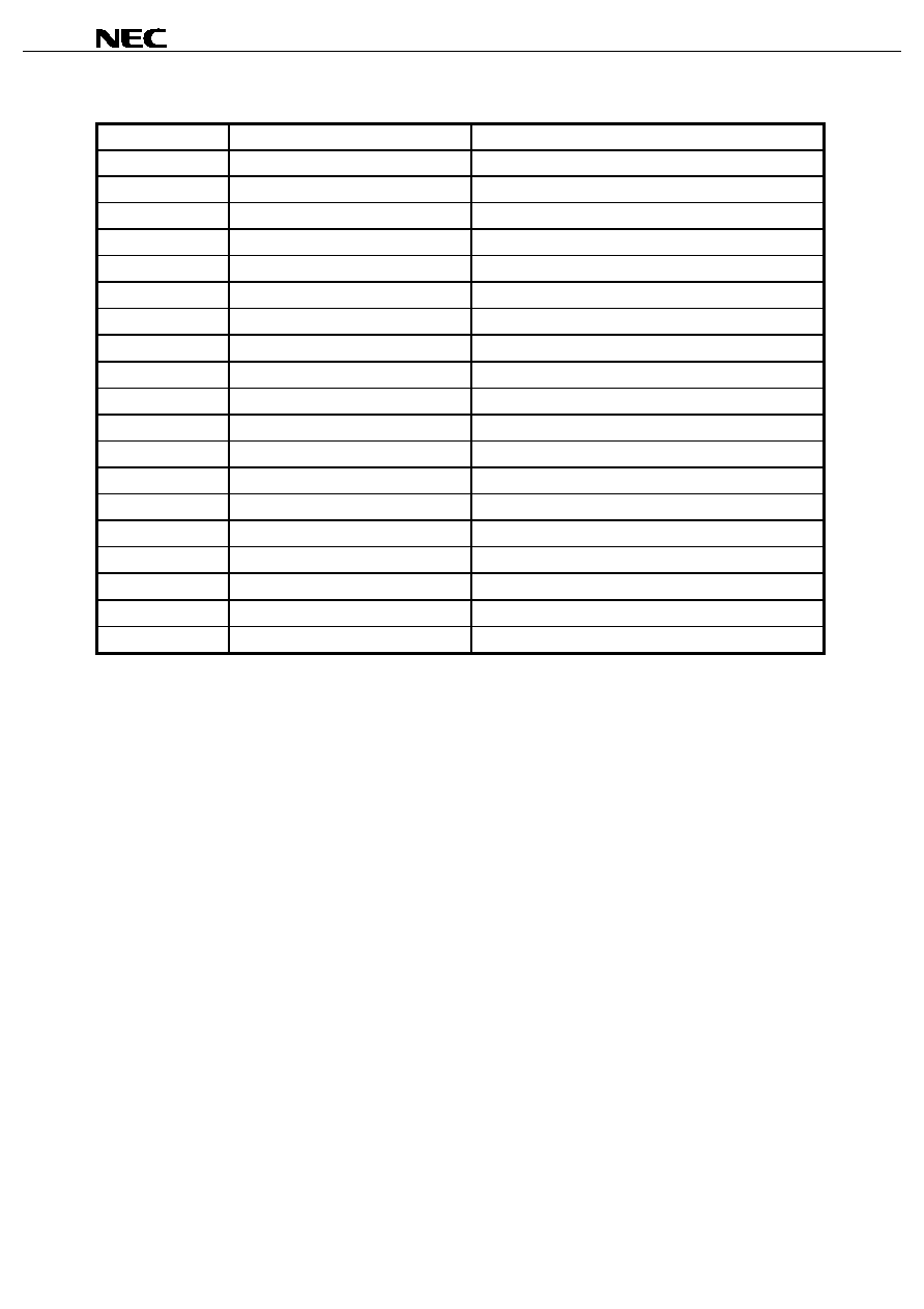
Pin Name and Functions [
µ
µ
µ
µ
PD464518ALS1]
Pin name
Description
Function
V
DD
Core Power Supply
Supplies power for RAM core
V
SS
Ground
V
DD
Q
Output Power Supply
Supplies power for output buffers
K, /K
Main Clock Input
SA0 to SA17
Synchronous Address Input
DQa1 to DQb9
Synchronous Data Input / Output
/SS
Synchronous Chip Select
Logically selects SRAM
/SW
Synchronous Byte Write Enable
Write command
/SBa
Synchronous Byte "a" Write Enable
Write DQa1 to DQa9
/SBb
Synchronous Byte "b" Write Enable
Write DQb1 to DQb9
/G
Asynchronous Output Enable
Asynchronous input
ZZ
Sleep Mode Enable
Enables sleep mode, active high
NC
No Connection
TMS
Test Mode Select (JTAG)
TDI
Test Data Input (JTAG)
TCK
Test Clock Input (JTAG)
TDO
Test Data Output (JTAG)
5
µ
µ
µ
µ
PD464518AL, 464536AL
Data Sheet M13609EJ4V0DS
Pin Name and Functions [
µ
µ
µ
µ
PD464536ALS1]
Pin name
Description
Function
V
DD
Core Power Supply
Supplies power for RAM core
V
SS
Ground
V
DD
Q
Output Power Supply
Supplies power for output buffers
K, /K
Main Clock
SA0 to SA16
Synchronous Address Input
DQa1 to DQd9
Synchronous Data Input / Output
/SS
Synchronous Chip Select
Logically selects SRAM
/SW
Synchronous Byte Write Enable
Write command
/SBa
Synchronous Byte "a" Write Enable
Write DQa1 to DQa9
/SBb
Synchronous Byte "b" Write Enable
Write DQb1 to DQb9
/SBc
Synchronous Byte "c" Write Enable
Write DQc1 to DQc9
/SBd
Synchronous Byte "d" Write Enable
Write DQd1 to DQd9
/G
Asynchronous Output Enable
Asynchronous input
ZZ
Sleep Mode Enable
Enables sleep mode, active high
NC
No Connection
TMS
Test Mode Select (JTAG)
TDI
Test Data Input (JTAG)
TCK
Test Clock Input (JTAG)
TDO
Test Data Output (JTAG)