The information in this document is subject to change without notice. Before using this document, please
confirm that this is the latest version.
Not all devices/types available in every country. Please check with local NEC representative for
availability and additional information.
©
1999
MOS INTEGRATED CIRCUIT
µ
µ
µ
µ
PD4416008
16M-BIT CMOS FAST SRAM
2M-WORD BY 8-BIT
DATA SHEET
Document No. M14080EJ4V0DS00 (4th edition)
Date Published December 2000 NS CP(K)
Printed in Japan
The mark
∑
∑
∑
∑
shows major revised points.
Description
The
µ
PD4416008 is a high speed, low power, 16,777,216 bits (2,097,152 words by 8 bits) CMOS static RAM.
Operating supply voltage is 3.3 V
±
0.3 V.
The
µ
PD4416008 is packaged in a 54-PIN PLASTIC TSOP (II) (10.16 mm (400))
Features
∑
2,097,152 words by 8 bits
∑
Fast access time : 15, 17 ns (MAX.)
∑
Output Enable input for easy application
Ordering Information
Part number
Package
Supply voltage
Access time
Supply current mA (MAX.)
V
ns (MAX.)
At operating
At standby
µ
PD4416008G5-A15-9JF
54-PIN PLASTIC TSOP (II)
3.3
±
0.3
15
230
10
µ
PD4416008G5-A17-9JF
(10.16 mm (400))
17
220
∑
∑

Data Sheet M14080EJ4V0DS
2
µ
µ
µ
µ
PD4416008
Pin Configuration (Marking Side)
/xxx indicates active low signal.
54-PIN PLASTIC TSOP (II) (10.16 mm (400))
[
µ
µ
µ
µ
PD4416008G5
-
-
-
-
xxx
-
-
-
-
9JF]
1
2
3
4
5
6
7
8
9
10
11
12
13
14
15
16
17
18
19
20
21
22
23
24
25
26
27
54
53
52
51
50
49
48
47
46
45
44
43
42
41
40
39
38
37
36
35
34
33
32
31
30
29
28
NC
V
CC
NC
I/O 7
GND
I/O 8
A0
A1
A2
A3
A4
NC
/CS
V
CC
/WE
NC
A5
A6
A7
A8
A9
I/O 1
V
CC
I/O 2
NC
GND
NC
NC
GND
NC
I/O 6
V
CC
I/O 5
A20
A19
A18
A17
A16
NC
/OE
GND
IC
A15
A14
A13
A12
A11
A10
I/O 4
GND
I/O 3
NC
V
CC
NC
A0 - A20
: Address Inputs
I/O1 - I/O8 : Data Inputs / Outputs
/CS
: Chip Select
/WE
: Write Enable
/OE
: Output Enable
V
CC
: Power supply
GND
: Ground
NC
: No connection
IC
: Internal connection
Note
Note
Leave this pin connect to GND.
Remark Refer to Package Drawing for 1-pin index mark.
Data Sheet M14080EJ4V0DS
3
µ
µ
µ
µ
PD4416008
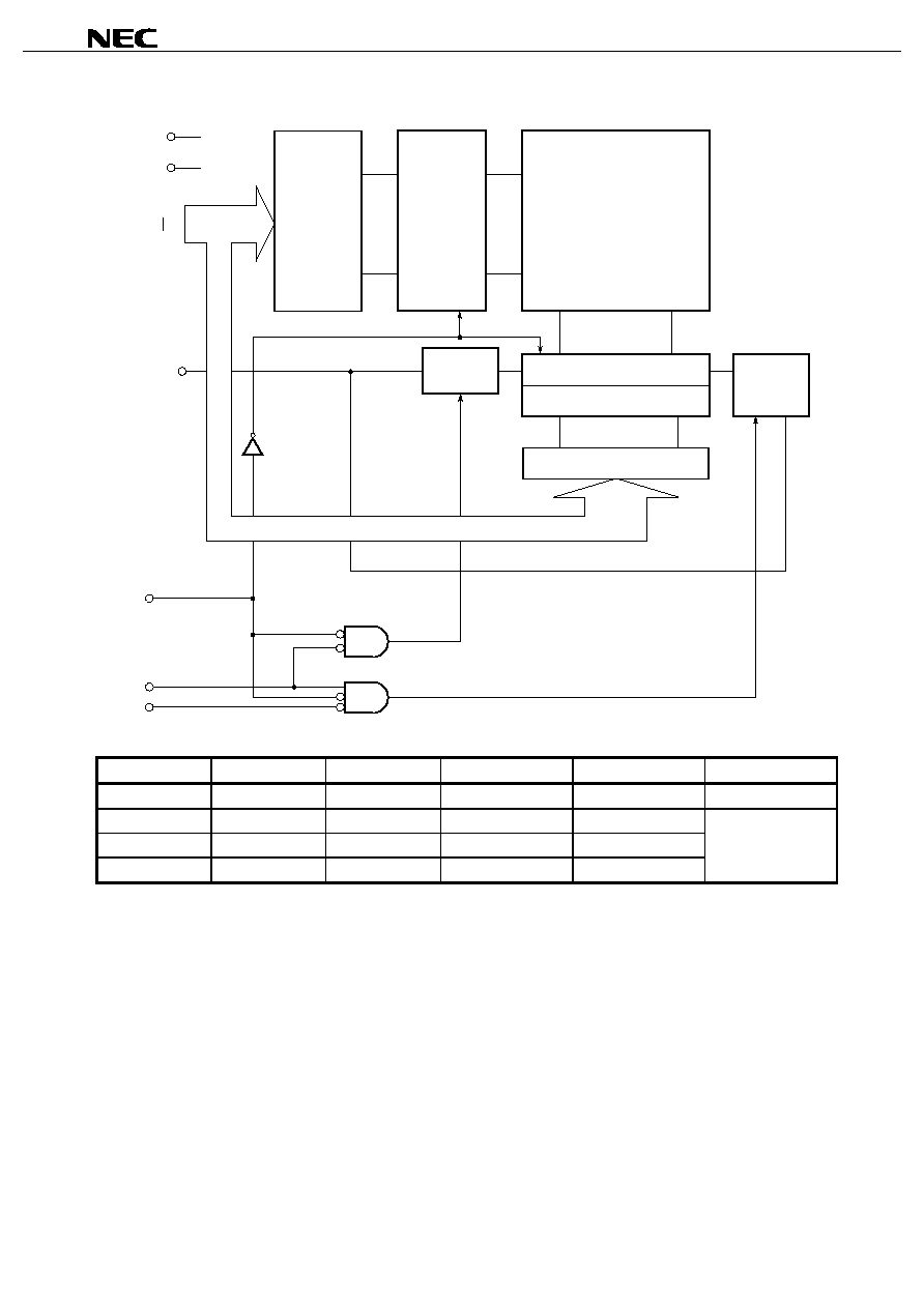
Block Diagram
Address buffer
Address
buffer
Row
decoder
Memory cell array
16,777,216 bits
Input data
controller
A0
A20
Sense amplifier /
Switching circuit
Column decoder
/CS
/WE
/OE
V
CC
GND
Output data
controller
I/O1 - I/O8
Truth Table
/CS
/OE
/WE
Mode
I/O
Supply current
H
◊
◊
Not selected
High impedance
I
SB
L
L
H
Read
D
OUT
I
CC
L
◊
L
Write
D
IN
L
H
H
Output disable
High impedance
Remark
◊
: Don't care

Data Sheet M14080EJ4V0DS
4
µ
µ
µ
µ
PD4416008
Electrical Specifications
Absolute Maximum Ratings
Parameter
Symbol
Condition
Rating
Unit
Supply voltage
V
CC
≠0.5
Note
to +4.0
V
Input / Output voltage
V
T
≠0.5
Note
to +4.0
V
Operating ambient temperature
T
A
0 to 70
∞
C
Storage temperature
T
stg
≠55 to +125
∞
C
Note ≠2.0 V (MIN.) (pulse width : 2 ns)
Caution
Exposing the device to stress above those listed in Absolute Maximum Rating could cause
permanent damage. The device is not meant to be operated under conditions outside the limits
described in the operational section of this specification. Exposure to Absolute Maximum Rating
conditions for extended periods may affect device reliability.
Recommended Operating Conditions
Parameter
Symbol
Condition
MIN.
TYP.
MAX.
Unit
Supply voltage
V
CC
3.0
3.3
3.6
V
High level input voltage
V
IH
2.0
V
CC
+ 0.3
V
Low level input voltage
V
IL
≠0.3
Note
+0.8
V
Operating ambient temperature
T
A
0
70
∞
C
Note ≠2.0 V (MIN.) (pulse width : 2 ns)
DC Characteristics (Recommended Operating Conditions Unless Otherwise Noted)
Parameter
Symbol
Test condition
MIN.
TYP.
MAX.
Unit
Input leakage current
I
LI
V
IN
= 0 V to V
CC
≠2
+2
µ
A
Output leakage current
I
LO
V
I/O
= 0 V to V
CC
, /CS = V
IH
or /OE = V
IH
or
≠2
+2
µ
A
/WE = V
IL
Operating supply current
I
CC
/CS = V
IL
, I
I/O
= 0 mA,
Cycle time : 15 ns
230
mA
Minimum cycle time
Cycle time : 17 ns
220
Standby supply current
I
SB
/CS = V
IH
, V
IN
= V
IH
or V
IL
, Minimum cycle time
80
mA
I
SB1
/CS
V
CC
≠ 0.2 V,
10
V
IN
0.2 V or V
IN
V
CC
≠ 0.2 V
High level output voltage
V
OH
I
OH
= ≠4.0 mA
2.4
V
Low level output voltage
V
OL
I
OL
= +8.0 mA
0.4
V
Remark
V
IN
: Input voltage, V
I/O
: Input / Output voltage
Capacitance (TA = 25
∞
∞
∞
∞
C, f = 1 MHz)
Parameter
Symbol
Test condition
MIN.
TYP.
MAX.
Unit
Input capacitance
C
IN
V
IN
= 0 V
6
pF
Input / Output capacitance
C
I/O
V
I/O
= 0 V
8
pF
Remarks 1. V
IN
: Input voltage, V
I/O
: Input / Output voltage
2. These parameters are periodically sampled and not 100% tested.
∑
∑
∑
∑

Data Sheet M14080EJ4V0DS
5
µ
µ
µ
µ
PD4416008
AC Characteristics (Recommended Operating Conditions Unless Otherwise Noted)
AC Test Conditions
LVTTL Interface
Input Waveform (Rise and Fall Time
3 ns)
Test Points
GND
3.0 V
1.5 V
1.5 V
Output Waveform
Test Points
1.5 V
1.5 V
Output Load
AC characteristics directed with the note should be measured with the output load shown in Figure 1 or Figure 2.
Figure 1
Figure 2
(for t
AA
, t
ACS
, t
OE
, t
OH
)
(for t
CLZ
, t
OLZ
, t
CHZ
, t
OHZ
, t
WHZ
, t
OW
)
V
TT
= +1.5 V
I/O (Output)
50
Z
O
= 50
30 pF
C
L
+3.3 V
I/O (Output)
317
5 pF
C
L
351
Remark
C
L
includes capacitances of the probe and jig, and stray capacitances.