The information in this document is subject to change without notice. Before using this document, please
confirm that this is the latest version.
Not all devices/types available in every country. Please check with local NEC representative for
availability and additional information.
©
2000
MOS INTEGRATED CIRCUIT
µ
µ
µ
µ
PD4443362
4M-BIT CMOS SYNCHRONOUS FAST STATIC RAM
128K-WORD BY 36-BIT
HSTL INTERFACE / REGISTER-REGISTER / LATE WRITE
DATA SHEET
Document No. M14439EJ2V0DS00 (2nd edition)
Date Published February 2001 NS CP(K)
Printed in Japan
The mark
5
5
5
5
shows major revised points.
Description
The
µ
PD4443362 is a 131,072 words by 36 bits synchronous static RAM fabricated with advanced CMOS
technology using Full-CMOS six-transistor memory cell.
The
µ
PD4443362 is suitable for applications which require synchronous operation, high-speed, low voltage, high-
density memory and wide bit configuration, such as cache and buffer memory.
The
µ
PD4443362 is packaged in 100-pin plastic LQFP with a 1.4 mm package thickness for high density and low
capacitive loading.
Features
∑
Fully synchronous operation
∑
HSTL Input / Output levels
∑
Fast clock access time : 3.8 ns (133 MHz)
∑
Asynchronous output enable control : /G
∑
Byte write control : /SBa (DQa1-9), /SBb (DQb1-9), /SBc (DQc1-9), /SBd (DQd1-9)
∑
Common I/O using three-state outputs
∑
Internally self-timed write cycle
∑
Late write with 1 dead cycle between Read-Write
∑
3.3 V (Chip) / 1.5 V (I/O) supply
∑
100-pin plastic LQFP package, 14 mm x 20 mm
∑
Sleep Mode : ZZ (Enables sleep mode, active high)
Ordering Information
Part number
Access time
Clock frequency
Package
µ
PD4443362GF-A75
3.8 ns
133 MHz
100-PIN PLASTIC LQFP (14 x 20)
5
5
5
5
5
5
5
5
Data Sheet M14439EJ2V0DS
3
µ
µ
µ
µ
PD4443362
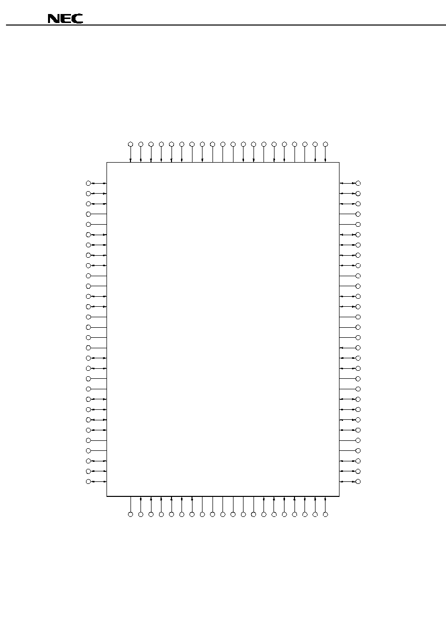
Pin Name and Functions
Pin name
Pin No.
Description
SA0 to SA16
37, 36, 35, 34, 33, 32, 100, 99, 82, 81, 44, Synchronous Address Input
45, 46, 47, 48, 49, 50
DQa1 to DQa9
63, 62, 59, 58, 57, 56, 53, 52, 51
Synchronous Data Input / Output
DQb1 to DQb9
68, 69, 72, 73, 74, 75, 78, 79, 80
DQc1 to DQc9
13, 12, 9, 8, 7, 6, 3, 2, 1
DQd1 to DQd9
18, 19, 22, 23, 24, 25, 28, 29, 30
/SS
98
Synchronous Chip Select
/SW
85
Synchronous Byte Write Enable
/SBa
Note1
93
Synchronous Byte "a" Write Enable
/SBb
Note1
95
Synchronous Byte "b" Write Enable
/SBc
Note1
96
Synchronous Byte "c" Write Enable
/SBd
Note1
97
Synchronous Byte "d" Write Enable
/G
86
Asynchronous Output Enable
ZZ
Note2
64
Asynchronous Sleep Mode
K, /K
89, 88
Main Clock Input
V
DD
15, 41, 65, 91
Core Power Supply
V
SS
17, 40, 67, 90
Ground
V
DD
Q
4, 11, 20, 27, 54, 61, 70, 77
Output Buffer Power Supply
V
SS
Q
5, 10, 21, 26, 55, 60, 71, 76
Output Buffer Ground
V
REF
38, 43, 87
Input Reference
NC
14, 16, 31, 39, 42, 66, 83, 84, 92, 94
No Connection
Notes 1. If Byte Write Operation is not used, Byte Write Pins (/SBa, /SBb, /SBc, /SBd) are to be tied to V
SS
.
2. If Sleep Mode is not used, ZZ Pin is to be tied to V
SS
.
Remark This device only supports Single Differential Clock, R / R Mode.
(R / R stands for Registered Input / Registered Output.)