The information in this document is subject to change without notice. Before using this document, please
confirm that this is the latest version.
Not all products and/or types are available in every country. Please check with NEC Electronics sales
representative for availability and additional information.
Document No. M15874EJ5V0DS00 (5th edition)
Date Published January 2003 NS CP (K)
Printed in Japan
MOS INTEGRATED CIRCUIT
µ
µ
µ
µ
PD4632312A-X
32M-BIT CMOS MOBILE SPECIFIED RAM
2M-WORD BY 16-BIT
EXTENDED TEMPERATURE OPERATION
PRELIMINARY DATA SHEET
The mark
# shows major revised points.
2001
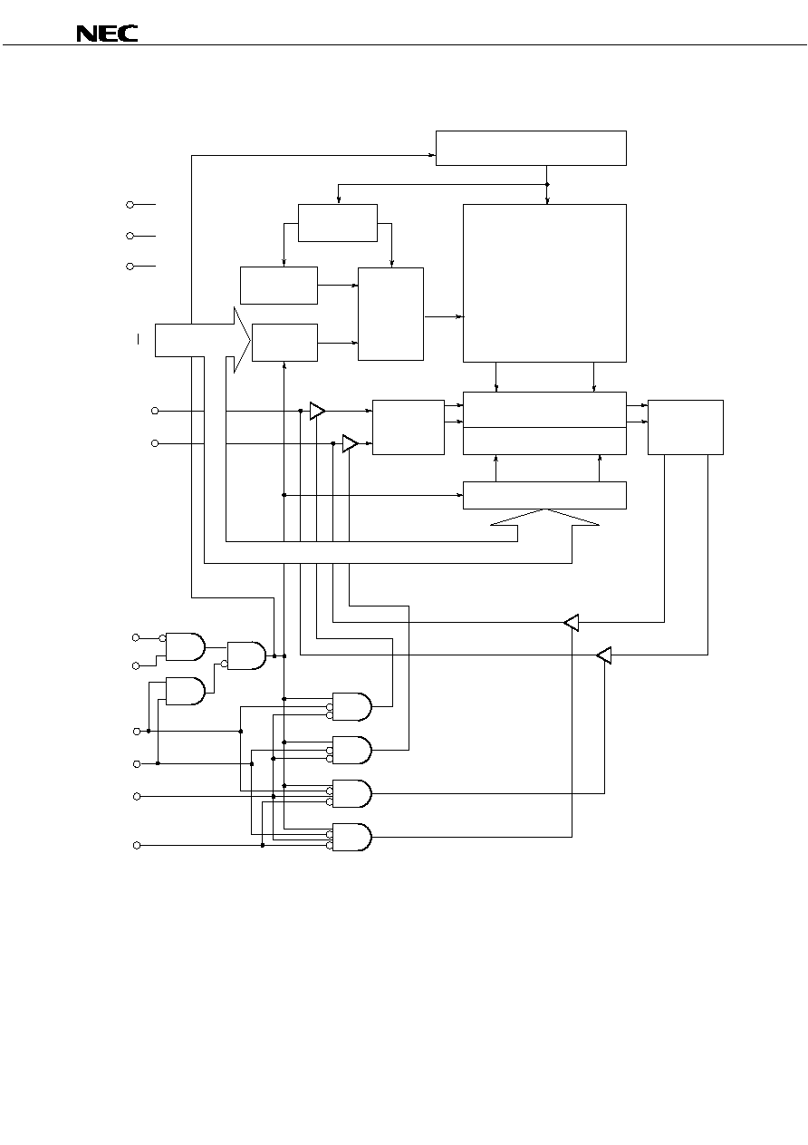
Description
The
µPD4632312A-X is a high speed, low power, 33,554,432 bits (2,097,152 words by 16 bits) CMOS Mobile
Specified RAM featuring Low Power Static RAM compatible function and pin configuration.
The
µPD4632312A-X is fabricated with advanced CMOS technology using one-transistor memory cell.
The
µPD4632312A-X is packed in 48-pin TAPE FBGA.
Features
∑ 2,097,152 words by 16 bits organization
∑ Fast access time: 60, 65, 75, 85 ns (MAX.)
∑ Fast page access time: 18, 25, 30 ns (MAX.)
∑ Byte data control: /LB (I/O0 to I/O7), /UB (I/O8 to I/O15)
∑ Low voltage operation: 2.7 to 3.1 V (-B60X, -B65X)
2.7 to 3.1 V (Chip), 1.65 to 2.1 V (I/O) (-BE75X, -BE85X)
∑ Operating ambient temperature: T
A
= ≠25 to +85 ∞C
∑ Output Enable input for easy application
∑ Chip Enable input: /CS pin
∑ Standby Mode input: MODE pin
∑ Standby Mode1: Normal standby (Memory cell data hold valid)
∑ Standby Mode2: Density of memory cell data hold is variable
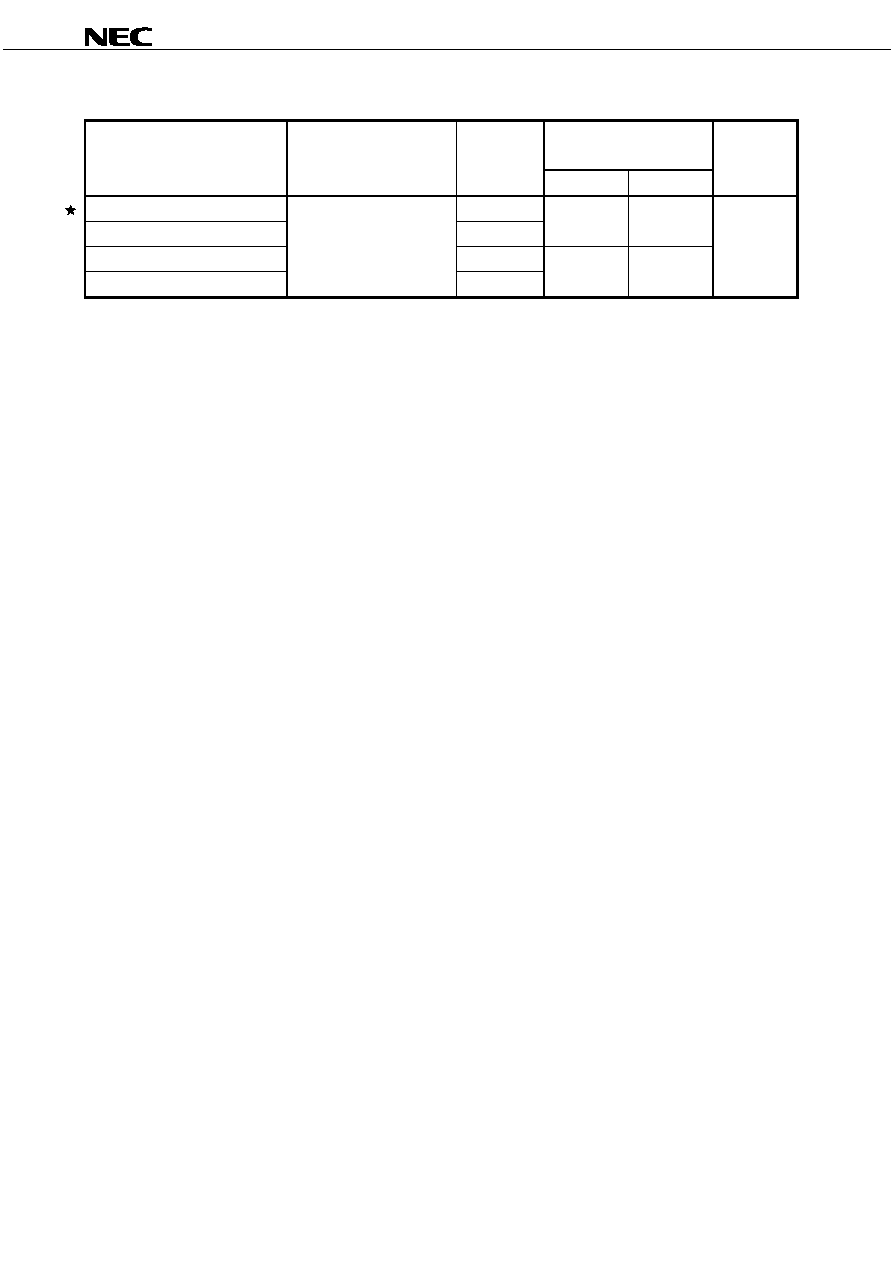
µPD4632312A
Access
Operating supply
Operating
Supply current
time
voltage
ambient
At operating
At standby
µA (MAX.)
ns (MAX.)
V
temperature mA (MAX.)
Density of data hold
Chip
I/O
∞C
32M bits 16M bits 8M bits 4M bits 0M bit
-B60X
Note
, -B65X
60, 65
2.7 to 3.1
≠
≠25 to +85
50
100
70
60
50
30
-BE75X
Note
, -BE85X
Note
75, 85
2.7 to 3.1 1.65 to 2.1
45
Note Under development

Preliminary Data Sheet M15874EJ5V0DS
3
µ
µ
µ
µPD4632312A-X
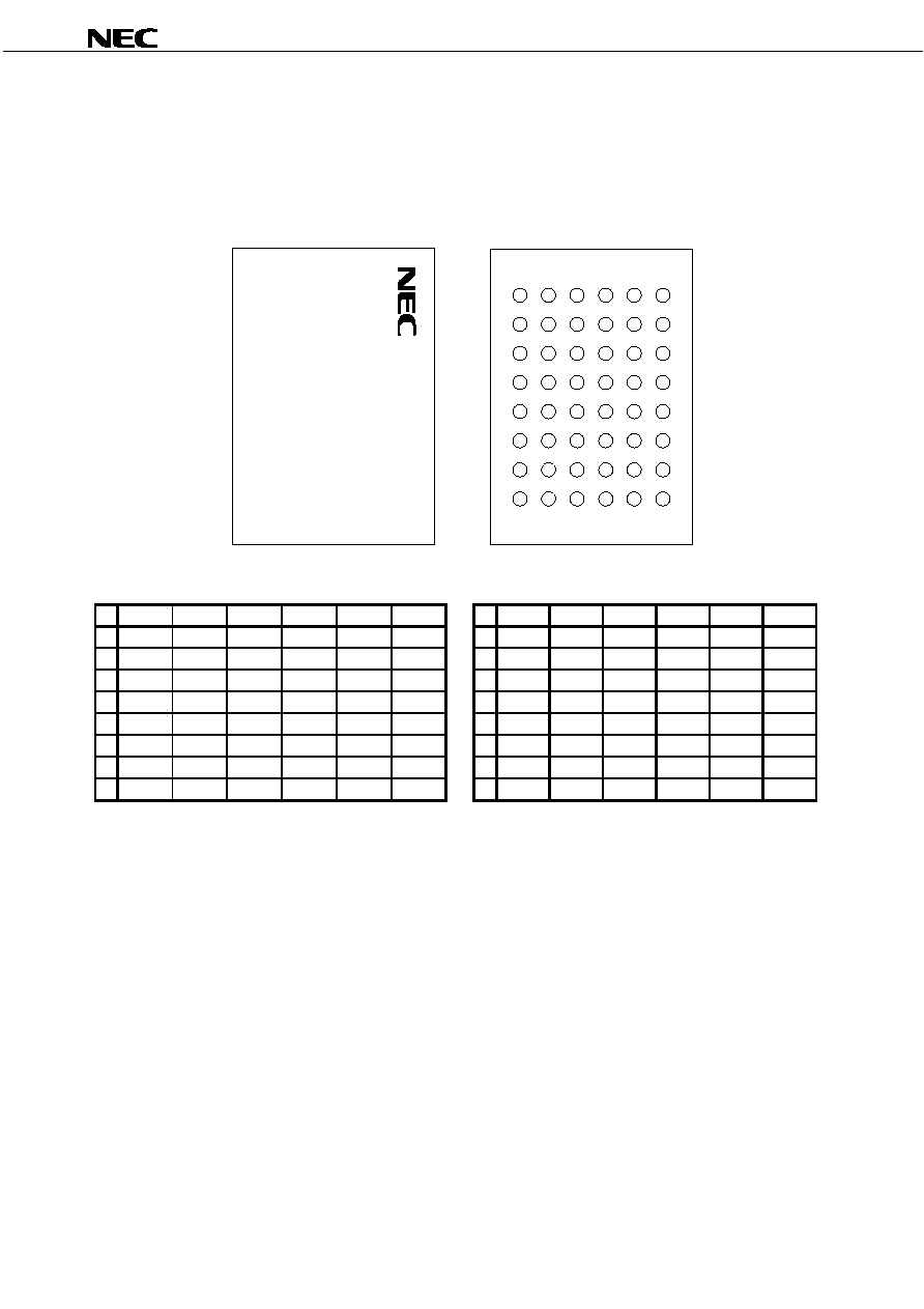
Pin Configurations
/xxx indicates active low signal.
48-pin TAPE FBGA (8 x 6)
[
µ
µ
µ
µPD4632312AF9-B60X-BC2 ]
[
µ
µ
µ
µPD4632312AF9-B65X-BC2 ]
A
B
C
D
E
F
G
H
1
2
3
4
5
6
Bottom View
6
5
4
3
2
1
Top View
1
2
3
4
5
6
6
5
4
3
2
1
A
/LB
/OE
A0
A1
A2
MODE
A
MODE
A2
A1
A0
/OE
/LB
B
I/O8
/UB
A3
A4
/CS
I/O0
B
I/O0
/CS
A4
A3
/UB
I/O8
C
I/O9
I/O10
A5
A6
I/O1
I/O2
C
I/O2
I/O1
A6
A5
I/O10
I/O9
D
GND
I/O11
A17
A7
I/O3
V
CC
D
V
CC
I/O3
A7
A17
I/O11
GND
E
V
CC
I/O12
NC
A16
I/O4
GND
E
GND
I/O4
A16
NC
I/O12
V
CC
F
I/O14
I/O13
A14
A15
I/O5
I/O6
F
I/O6
I/O5
A15
A14
I/O13
I/O14
G
I/O15
A19
A12
A13
/WE
I/O7
G
I/O7
/WE
A13
A12
A19
I/O15
H
A18
A8
A9
A10
A11
A20
H
A20
A11
A10
A9
A8
A18
Note Some signals can be applied because this pin is not internally connected.
Remark Refer to Package Drawing for the index mark.
A0 to A20
: Address inputs
I/O0 to I/O15 : Data inputs / outputs
/CS
: Chip select
MODE
: Standby mode
/WE
: Write enable
/OE
: Output enable
/LB, /UB
: Byte data select
V
CC
: Power supply
GND
: Ground
NC
Note
: No connection
Preliminary Data Sheet M15874EJ5V0DS
4
µ
µ
µ
µPD4632312A-X
48-pin TAPE FBGA (8 x 6)
[
µ
µ
µ
µPD4632312AF9-BE75X-BC2 ]
[
µ
µ
µ
µPD4632312AF9-BE85X-BC2 ]
A
B
C
D
E
F
G
H
1
2
3
4
5
6
Bottom View
6
5
4
3
2
1
Top View
1
2
3
4
5
6
6
5
4
3
2
1
A
/LB
/OE
A0
A1
A2
MODE
A
MODE
A2
A1
A0
/OE
/LB
B
I/O8
/UB
A3
A4
/CS
I/O0
B
I/O0
/CS
A4
A3
/UB
I/O8
C
I/O9
I/O10
A5
A6
I/O1
I/O2
C
I/O2
I/O1
A6
A5
I/O10
I/O9
D
GND
I/O11
A17
A7
I/O3
V
CC
D
V
CC
I/O3
A7
A17
I/O11
GND
E
V
CC
Q
I/O12
NC
A16
I/O4
GND
E
GND
I/O4
A16
NC
I/O12
V
CC
Q
F
I/O14
I/O13
A14
A15
I/O5
I/O6
F
I/O6
I/O5
A15
A14
I/O13
I/O14
G
I/O15
A19
A12
A13
/WE
I/O7
G
I/O7
/WE
A13
A12
A19
I/O15
H
A18
A8
A9
A10
A11
A20
H
A20
A11
A10
A9
A8
A18
Note Some signals can be applied because this pin is not internally connected.
Remark Refer to Package Drawing for the index mark.
A0 to A20
: Address inputs
I/O0 to I/O15 : Data inputs / outputs
/CS
: Chip Select
MODE
: Standby mode
/WE
: Write enable
/OE
: Output enable
/LB, /UB
: Byte data select
V
CC
: Power supply
V
CC
Q
: Input / Output power supply
GND
: Ground
NC
Note
: No connection