Document Outline
- COVER
- Features
- Ordering Information
- Pin Configurations
- Block Diagram
- Electrical Specifications
- Package Drawings

The information in this document is subject to change without notice. Before using this document, please
confirm that this is the latest version.
Not all products and/or types are available in every country. Please check with an NEC Electronics
sales representative for availability and additional information.
MOS INTEGRATED CIRCUIT
µPD23C128040BL, 23C128080BL
128M-BIT MASK-PROGRAMMABLE ROM
16M-WORD BY 8-BIT (BYTE MODE) / 8M-WORD BY 16-BIT (WORD MODE)
PAGE ACCESS MODE
DATA SHEET
Document No. M16048EJ2V0DS00 (2nd edition)
Date Published February 2003 NS CP (K)
Printed in Japan
The mark shows major revised points.
2002
Description
The
µPD23C128040BL and µPD23C128080BL are a 134,217,728 bits mask-programmable ROM. The word
organization is selectable (BYTE mode : 16,777,216 words by 8 bits, WORD mode : 8,388,608 words by 16 bits).
With 44-pin PLASTIC SOP package products, only WORD mode can be used; it is not possible to switch to BYTE
mode.
The active levels of OE (Output Enable Input) can be selected with mask-option.
The
µPD23C128040BL and µPD23C128080BL are packed in 48-pin PLASTIC TSOP(I) and 44-pin PLASTIC SOP.
Features
∑ Word organization
16,777,216 words by 8 bits (BYTE mode)
Note
8,388,608 words by 16 bits (WORD mode)
Note
Note
With 44-pin PLASTIC SOP package products, only WORD mode can be used.
It is not possible to switch to BYTE mode.
∑ Page access mode
BYTE mode : 8 byte random page access (
µPD23C128040BL)
16 byte random page access (
µPD23C128080BL)
WORD mode : 4 word random page access
(
µPD23C128040BL)
8 word random page access (
µPD23C128080BL)
∑ Operating supply voltage : V
CC
= 2.7 to 3.6 V
Operating supply
Access time /
Power supply current (Active mode)
Standby current
voltage
Page access time
mA (MAX.)
(CMOS level input)
V
CC
ns (MAX.)
µPD23C128040BL µPD23C128080BL
µA (MAX.)
3.0 V
± 0.3 V
120 / 25
50
70
30
3.3 V
± 0.3 V
100 / 25
55
75

Data Sheet M16048EJ2V0DS
2
µPD23C128040BL, 23C128080BL
Ordering Information
Part Number
Package
µPD23C128040BLGY-xxx-MJH
48-pin PLASTIC TSOP(I) (12x18) (Normal bent)
µPD23C128040BLGY-xxx-MKH
48-pin PLASTIC TSOP(I) (12x18) (Reverse bent)
µPD23C128040BLGX-xxx
44-pin PLASTIC SOP (15.24 mm (600))
µPD23C128080BLGY-xxx-MJH
48-pin PLASTIC TSOP(I) (12x18) (Normal bent)
µPD23C128080BLGY-xxx-MKH
48-pin PLASTIC TSOP(I) (12x18) (Reverse bent)
µPD23C128080BLGX-xxx
44-pin PLASTIC SOP (15.24 mm (600))
(xxx : ROM code suffix No.)

Data Sheet M16048EJ2V0DS
3
µPD23C128040BL, 23C128080BL
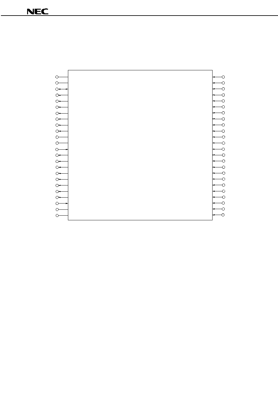
Pin Configurations
/xxx indicates active low signal.
48-pin PLASTIC TSOP(I) (12 x 18) (Normal bent)
[
µ
µ
µ
µPD23C128040BLGY-xxx-MJH ]
[
µ
µ
µ
µPD23C128080BLGY-xxx-MJH ]
Marking Side
WORD, /BYTE
A16
A15
A14
A13
A12
A11
A10
A9
A8
A19
A21
A20
A18
A17
A7
A6
A5
A4
A3
A2
A1
A0
/CE
GND
GND
O15, A≠1
O7
O14
O6
O13
O5
O12
O4
V
CC
V
CC
A22
O11
O3
O10
O2
O9
O1
O8
O0
/OE or OE or DC
GND
GND
1
2
3
4
5
6
7
8
9
10
11
12
13
14
15
16
17
18
19
20
21
22
23
24
48
47
46
45
44
43
42
41
40
39
38
37
36
35
34
33
32
31
30
29
28
27
26
25
A0 to A22
: Address inputs
O0 to O7, O8 to O14 : Data outputs
O15, A≠1
: Data output 15 (WORD mode),
LSB Address input (BYTE mode)
WORD, /BYTE
: Mode select
/CE
: Chip Enable
/OE or OE
: Output Enable
V
CC
: Supply voltage
GND
: Ground
DC
: Don't Care
Remark Refer to Package Drawings for the 1-pin index mark.
Data Sheet M16048EJ2V0DS
4
µPD23C128040BL, 23C128080BL
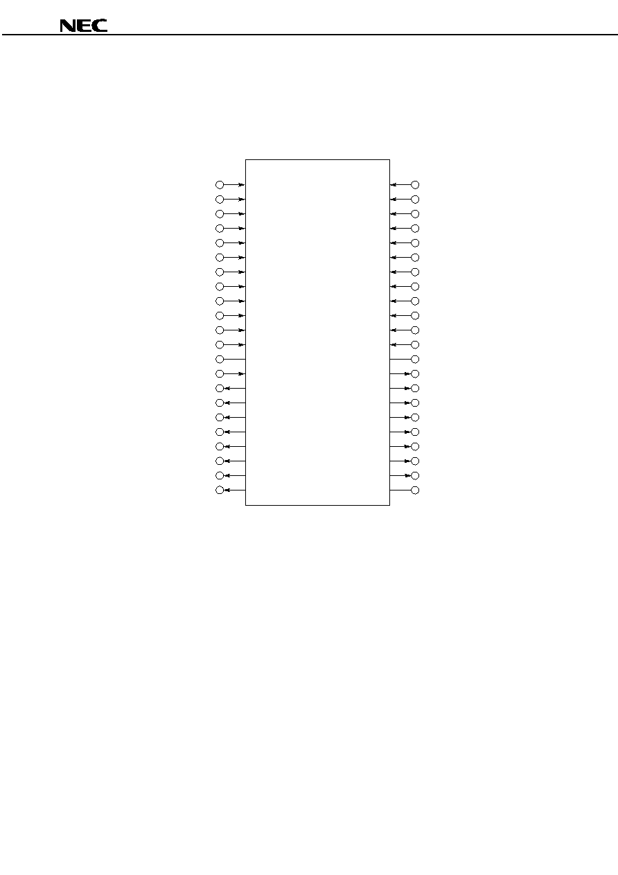
48-pin PLASTIC TSOP(I) (12 x 18) (Reverse bent)
[
µ
µ
µ
µPD23C128040BLGY-xxx-MKH ]
[
µ
µ
µ
µPD23C128080BLGY-xxx-MKH ]
Marking Side
WORD, /BYTE
A16
A15
A14
A13
A12
A11
A10
A9
A8
A19
A21
A20
A18
A17
A7
A6
A5
A4
A3
A2
A1
A0
/CE
GND
GND
O15, A≠1
O7
O14
O6
O13
O5
O12
O4
V
CC
V
CC
A22
O11
O3
O10
O2
O9
O1
O8
O0
/OE or OE or DC
GND
GND
1
2
3
4
5
6
7
8
9
10
11
12
13
14
15
16
17
18
19
20
21
22
23
24
48
47
46
45
44
43
42
41
40
39
38
37
36
35
34
33
32
31
30
29
28
27
26
25
A0 to A22
: Address inputs
O0 to O7, O8 to O14 : Data outputs
O15, A≠1
: Data output 15 (WORD mode),
LSB Address input (BYTE mode)
WORD, /BYTE
: Mode select
/CE
: Chip Enable
/OE or OE
: Output Enable
V
CC
: Supply voltage
GND
: Ground
DC
: Don't Care
Remark Refer to Package Drawings for the 1-pin index mark.
Data Sheet M16048EJ2V0DS
5
µPD23C128040BL, 23C128080BL
44-pin PLASTIC SOP (15.24 mm (600))
[
µ
µ
µ
µPD23C128040BLGX-xxx ]
[
µ
µ
µ
µPD23C128080BLGX-xxx ]
Marking Side
1
2
3
4
5
6
7
8
9
10
11
12
13
14
15
16
17
18
19
20
21
22
A21
A18
A17
A7
A6
A5
A4
A3
A2
A1
A0
/CE
GND
/OE or OE or DC
O0
O8
O1
O9
O2
O10
O3
O11
44
43
42
41
40
39
38
37
36
35
34
33
32
31
30
29
28
27
26
25
24
23
A20
A19
A8
A9
A10
A11
A12
A13
A14
A15
A16
A22
GND
O15
O7
O14
O6
O13
O5
O12
O4
V
CC
A0 to A22
: Address inputs
O0 to O15
: Data outputs
/CE
: Chip Enable
/OE or OE
: Output Enable
V
CC
: Supply voltage
GND
: Ground
DC
: Don't Care
Remarks 1. Refer to Package Drawings for the 1-pin index mark.
2. With 44-pin PLASTIC SOP package products, only WORD mode (8,388,608 words x 16 bits) can
be used. There is no mode select (WORD, /BYTE) pin.