©
1999
MOS INTEGRATED CIRCUIT
MC-458CA721ESA, 458CA721PSA
8M-WORD BY 72-BIT
SYNCHRONOUS DYNAMIC RAM MODULE (SO DIMM)
Document No. M14494EJ2V0DS00 (2nd edition)
Date Published February 2000 NS CP(K)
Printed in Japan
DATA SHEET
The information in this document is subject to change without notice. Before using this document, please
confirm that this is the latest version.
Not all devices/types available in every country. Please check with local NEC representative for
availability and additional information.
The mark
∑
∑
∑
∑
shows major revised points.
Description
The MC-458CA721ESA and MC-458CA721PSA are 8,388,608 words by 72 bits synchronous dynamic RAM module
(Small Outline DIMM) on which 5 pieces of 128M SDRAM:
µ
PD45128163 are assembled.
These modules provide high density and large quantities of memory in a small space without utilizing the surface-
mounting technology on the printed circuit board.
Decoupling capacitors are mounted on power supply line for noise reduction.
Features
∑
8,388,608 words by 72 bits organization (ECC type)
∑
Clock frequency and access time from CLK
Part number
/CAS latency
Clock frequency (MAX.)
Access time from CLK (MAX.)
MC-458CA721ESA-A80
CL = 3
125
MHz
6
ns
CL = 2
100
MHz
6
ns
MC-458CA721ESA-A10
CL = 3
100 MHz
6
ns
CL = 2
77 MHz
7
ns
MC-458CA721PSA-A80
CL = 3
125
MHz
6
ns
CL = 2
100
MHz
6
ns
MC-458CA721PSA-A10
CL = 3
100 MHz
6
ns
CL = 2
77 MHz
7
ns
∑
Fully Synchronous Dynamic RAM, with all signals referenced to a positive clock edge
∑
Pulsed interface
∑
Possible to assert random column address in every cycle
∑
Quad internal banks controlled by BA0, BA1 (Bank Select)
∑
Programmable burst-length (1, 2, 4, 8 and Full Page)
∑
Programmable wrap sequence (Sequential
/
Interleave)
∑
Programmable /CAS latency (2, 3)
∑
Automatic precharge and controlled precharge
∑
CBR (Auto) refresh and self refresh
∑
Single 3.3
V
±
0.3
V power supply
∑
LVTTL compatible
∑
4,096 refresh cycles/64
ms
∑
Burst termination by Burst Stop command and Precharge command
∑
144-pin small outline dual in-line memory module (Pin pitch = 0.8
mm)
∑
Unbuffered type
∑
Serial PD
5
5
Data Sheet M14494EJ2V0DS00
2
MC-458CA721ESA, 458CA721PSA
Ordering Information
Part number
Clock frequency
MHz (MAX.)
Package
Mounted devices
MC-458CA721ESA-A80
125 MHz
144-pin Small Outline DIMM
5 piece of
µ
PD45128163G5 (Rev. E)
(Socket Type)
(10.16mm (400) TSOP (II))
MC-458CA721ESA-A10
100 MHz
Edge connector: Gold plated
31.75 mm height
MC-458CA721PSA-A80
125 MHz
5 piece of
µ
PD45128163G5 (Rev. P)
(10.16mm (400) TSOP (II))
MC-458CA721PSA-A10
100 MHz
5
5
Data Sheet M14494EJ2V0DS00
3
MC-458CA721ESA, 458CA721PSA
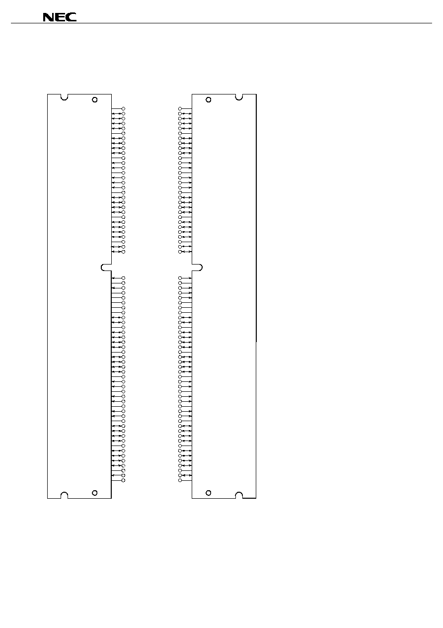
Pin Configuration
144-pin Dual In-line Memory Module Socket Type (Edge connector: Gold plated)
1
3
5
7
9
11
13
15
17
19
21
23
25
27
29
31
33
35
37
39
41
43
45
47
49
51
53
55
57
59
Vss
DQ 0
DQ 1
DQ 2
DQ 3
DQ 4
DQ 5
DQ 6
DQ 7
Vss
DQMB0
DQMB1
A0
A1
A2
Vss
DQ 8
DQ 9
DQ 10
DQ 11
DQ 12
DQ 13
DQ 14
DQ 15
Vss
CB 0
CB 1
61
63
65
67
69
71
73
75
77
79
81
83
85
87
89
91
93
95
97
99
101
103
105
107
109
111
113
115
117
119
121
123
125
127
129
131
133
135
137
139
141
143
CLK0
Vcc
/RAS
/WE
/CS0
NC
NC
Vss
CB 2
CB 3
DQ 16
DQ 17
DQ 18
DQ 19
Vss
DQ 20
DQ 21
DQ 22
DQ 23
Vcc
A6
A8
Vss
A9
A10
Vcc
DQMB2
DQMB3
Vss
DQ 24
DQ 25
DQ 26
DQ 27
DQ 28
DQ 29
DQ 30
DQ 31
Vss
SDA
2
4
6
8
10
12
14
16
18
20
22
24
26
28
30
32
34
36
38
40
42
44
46
48
50
52
54
56
58
60
Vss
DQ 32
DQ 33
DQ 34
DQ 35
Vcc
DQ 36
DQ 37
DQ 38
DQ 39
Vss
DQMB4
DQMB5
Vcc
A3
A4
A5
Vss
DQ 40
DQ 41
DQ 42
DQ 43
Vcc
DQ 44
DQ 45
DQ 46
DQ 47
Vss
CB 4
CB 5
62
64
66
68
70
72
74
76
78
80
82
84
86
88
90
92
94
96
98
100
102
104
106
108
110
112
114
116
118
120
122
124
126
128
130
132
134
136
138
140
142
144
CKE0
Vcc
/CAS
NC
NC
NC
CLK1
Vss
CB 6
CB 7
Vcc
DQ 48
DQ 49
DQ 50
DQ 51
Vss
DQ 52
DQ 53
DQ 54
DQ 55
Vcc
A7
BA0 (A13)
Vss
BA1 (A12)
A11
Vcc
DQMB6
DQMB7
Vss
DQ 56
DQ 57
DQ 58
DQ 59
Vcc
DQ 60
DQ 61
DQ 62
DQ 63
Vss
SCL
Vcc
CC
V
CC
V
CC
V
CC
V
CC
V
CC
V
/xxx indicates active low signal.
A0 - A11
: Address Inputs
[Row: A0 - A11, Column: A0 - A8]
BA0(A13), BA1(A12) : SDRAM Bank Select
DQ0 - DQ63
: Data Inputs/Outputs
CB0 - CB7
: Data Inputs/Outputs
CLK0, CLK1
: Clock Input
CKE0
: Clock Enable Input
/CS0
: Chip Select Input
/RAS
: Row Address Strobe
/CAS
: Column Address Strobe
/WE
: Write Enable
DQMB0 - DQMB7
: DQ Mask Enable
SDA
: Serial Data I/O for PD
SCL
: Clock Input for PD
V
CC
: Power Supply
V
SS
: Ground
NC
: No Connection
Data Sheet M14494EJ2V0DS00
4
MC-458CA721ESA, 458CA721PSA
Block Diagram
/WE
/CS0
A0 - A11
A0 - A11 : D0 - D4
V
CC
D0 - D4
D0 - D4
SERIAL PD
SCL
SDA
A0 A1 A2
DQMB0
DQMB1
/CS
/WE
D0
LDQM
UDQM
DQ 0
DQ 1
DQ 4
DQ 3
DQ 2
DQ 5
DQ 6
DQ 7
/CS
/WE
D1
LDQM
UDQM
DQMB6
DQMB7
/CS
/WE
D4
LDQM
UDQM
DQMB4
DQMB5
/CS
/WE
D3
LDQM
UDQM
DQ 0
DQ 1
DQ 2
DQ 5
DQ 4
DQ 3
DQ 6
DQ 7
DQ 8
DQ 9
DQ 10
DQ 13
DQ 12
DQ 11
DQ 14
DQ 15
DQ 8
DQ 9
DQ 12
DQ 11
DQ 10
DQ 13
DQ 14
DQ 15
CB 0
CB 1
CB 2
CB 5
CB 4
CB 3
CB 6
CB 7
DQ 8
DQ 9
DQ 12
DQ 11
DQ 10
DQ 13
DQ 14
DQ 15
DQ 0
DQ 1
DQ 4
DQ 3
DQ 2
DQ 5
DQ 6
DQ 7
DQ 0
DQ 1
DQ 4
DQ 3
DQ 2
DQ 5
DQ 6
DQ 7
DQ 8
DQ 9
DQ 12
DQ 11
DQ 10
DQ 13
DQ 14
DQ 15
DQ 48
DQ 49
DQ 50
DQ 53
DQ 52
DQ 51
DQ 54
DQ 55
DQ 56
DQ 57
DQ 58
DQ 61
DQ 60
DQ 59
DQ 62
DQ 63
DQ 32
DQ 33
DQ 34
DQ 37
DQ 36
DQ 35
DQ 38
DQ 39
DQ 40
DQ 41
DQ 42
DQ 45
DQ 44
DQ 43
DQ 46
DQ 47
DQ 0
DQ 1
DQ 4
DQ 3
DQ 2
DQ 5
DQ 6
DQ 7
DQ 8
DQ 9
DQ 12
DQ 11
DQ 10
DQ 13
DQ 14
DQ 15
/RAS
/RAS : D0 - D4
/CAS
/CAS : D0 - D4
CKE0
CKE : D0 - D4
V
SS
BA0
A13 : D0 - D4
CLK0
CLK1
CLK : D0 - D4
10
10 pF
C
BA1
A12 : D0 - D4
DQMB2
DQMB3
/CS
/WE
D2
LDQM
UDQM
DQ 16
DQ 17
DQ 18
DQ 21
DQ 20
DQ 19
DQ 22
DQ 23
DQ 24
DQ 25
DQ 26
DQ 29
DQ 28
DQ 27
DQ 30
DQ 31
DQ 8
DQ 9
DQ 12
DQ 11
DQ 10
DQ 13
DQ 14
DQ 15
DQ 0
DQ 1
DQ 4
DQ 3
DQ 2
DQ 5
DQ 6
DQ 7
Remarks 1. D0 ≠ D4:
µ
PD45128163 (2M words x 16 bits x 4 banks)
2. The value of all resistors is 10
.
Data Sheet M14494EJ2V0DS00
5
MC-458CA721ESA, 458CA721PSA
Electrical Specifications
∑
All voltages are referenced to V
SS
(GND).
∑
After power up, wait more than 100
µ
s and then, execute power on sequence and CBR (Auto) refresh before proper
device operation is achieved.
Absolute Maximum Ratings
Parameter
Symbol
Condition
Rating
Unit
Voltage on power supply pin relative to GND
V
CC
≠0.5 to +4.6
V
Voltage on input pin relative to GND
V
T
≠0.5 to +4.6
V
Short circuit output current
I
O
50
mA
Power dissipation
P
D
5
W
Operating ambient temperature
T
A
0 to 70
∞
C
Storage temperature
T
stg
≠55 to +125
∞
C
Caution
Exposing the device to stress above those listed in Absolute Maximum Ratings could cause
permanent damage. The device is not meant to be operated under conditions outside the limits
described in the operational section of this specification. Exposure to Absolute Maximum Rating
conditions for extended periods may affect device reliability.
Recommended Operating Conditions
Parameter
Symbol
Condition
MIN.
TYP.
MAX.
Unit
Supply voltage
V
CC
3.0
3.3
3.6
V
High level input voltage
V
IH
2.0
V
CC
+
0.3
V
Low level input voltage
V
IL
≠0.3
+0.8
V
Operating ambient temperature
T
A
0
70
∞
C
Capacitance (T
A
= 25
∞
∞
∞
∞
C, f = 1 MHz)
Parameter
Symbol
Test condition
MIN.
TYP.
MAX.
Unit
Input capacitance
C
I1
A0 - A11, BA0(A13), BA1(A12),
/RAS, /CAS, /WE
17
34
pF
C
I2
CLK0
23
37
C
I3
CKE0
18
30
C
I4
/CS0
18
30
C
I5
DQMB0 - DQMB7
5
16.5
Data input/output capacitance
C
I/O
DQ0 - DQ63, CB0 - CB7
5
13
pF