
The information in this document is subject to change without notice. Before using this document, please
confirm that this is the latest version.
Not all devices/types available in every country. Please check with local NEC representative for
availability and additional information.
HETERO JUNCTION FIELD EFFECT TRANSISTOR
NE3210S01
X to Ku BAND SUPER LOW NOISE AMPLIFER
N-CHANNEL HJ-FET
Document No. P14067EJ2V0DS00 (2nd edition)
Date Published November 1999 N CP(K)
Printed in Japan
DATA SHEET
1999
©
The mark shows major revised points.
DESCRIPTION
The NE3210S01 is a Hetero Junction FET that utilizes the hetero junction to create high mobility electrons. Its
excellent low noise and associated gain make it suitable for DBS and another commercial systems.
FEATURES
∑
Super Low Noise Figure & High Associated Gain
NF = 0.35 dB TYP. Ga = 13.5 dB TYP. at f = 12 GHz
∑
Gate Length: Lg
0.20
µ
m
∑
Gate Width : Wg = 160
µ
m
ORDERING INFORMATION (PLAN)
Part Number
Supplying Form
Marking
NE3210S01-T1
Tape & reel 1 000 pcs./reel
NE3210S01-T1B
Tape & reel 4 000 pcs./reel
K
Remark For sample order, please contact your local NEC sales office. (Part number for sample order: NE3210S01)
ABSOLUTE MAXIMUM RATINGS (T
A
= 25∞C)
Parameter
Symbol
Ratings
Unit
Drain to Source Voltage
V
DS
4.0
V
Gate to Source Voltage
V
GS
≠3.0
V
Drain Current
I
D
IDSS
mA
Gate Current
I
G
100
µ
A
Total Power Dissipation
P
tot
165
mW
Channel Temperature
T
ch
125
∞C
Storage Temperature
T
stg
≠65 to +125
∞C
RECOMMENDED OPERATING CONDITIONS (T
A
= +25∞C)
Characteristics
Symbol
MIN.
TYP.
MAX.
Unit
Drain to Source Voltage
V
DS
1
2
3
V
Drain Current
I
D
5
10
15
mA
Input Power
P
in
≠
≠
0
dBm

Data Sheet P14067EJ2V0DS00
2
NE3210S01
ELECTRICAL CHARACTERISTICS (T
A
= +25 ∞C)
Characteristics
Symbol
Test Conditions
MIN.
TYP.
MAX.
Unit
Gate to Source Leak Current
I
GSO
V
GS
= ≠3 V
≠
0.5
10
µ
A
Saturated Drain Current
I
DSS
V
DS
= 2 V, V
GS
= 0 V
15
40
70
mA
Gate to Source Cut off Voltage
V
GS (off)
V
DS
= 2 V, I
DS
= 100
µ
A
≠0.2
≠0.7
≠2.0
V
Transconductance
g
m
V
DS
= 2 V, I
DS
= 10 mA
40
55
≠
mS
Noise Figure
NF
≠
0.35
0.45
dB
Associated Gain
G
a
V
DS
= 2 V, I
DS
= 10 mA
f = 12 GHz
12.0
13.5
≠
dB
Data Sheet P14067EJ2V0DS00
3
NE3210S01
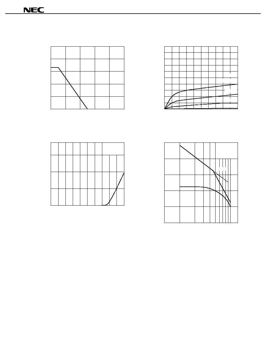
TYPICAL CHARACTERISTICS (T
A
= +25 ∞C)
250
200
150
100
50
0
50
100
150
200
250
TOTAL POWER DISSIPATION vs.
AMBIENT TEMPERATURE
Ambient Temperature T
A
(
∞
C)
Total Power Dissipation P
tot
(mW)
DRAIN CURRENT vs.
DRAIN TO SOURCE VOLTAGE
Drain to Source Voltage V
DS
(V)
100
80
60
40
20
0
2.0
1.0
Drain Current I
D
(mA)
V
GS
= 0 V
≠0.2 V
≠0.4 V
≠0.6 V
60
40
20
0
≠2.0
≠1.0
0
DRAIN CURRENT vs.
GATE TO SOURCE VOLTAGE
Gate to Source Voltage V
GS
(V)
Drain Current I
D
(mA)
Frequency f (GHz)
Maximum Stable Gain MSG. (dB)
Maximum Available Gain MAG. (dB)
Forward Insertion Gain |S
21s
|
2
(dB)
V
DS
= 2 V
MAXIMUM AVAILABLE GAIN, FORWARD
INSERTION GAIN vs. FREQUENCY
24
20
16
12
8
4
1
30
2
4
20
6
8 10
14
V
DS
= 2 V
I
D
= 10 mA
MSG.
MAG.
|S
21S
|
2

Data Sheet P14067EJ2V0DS00
4
NE3210S01
Gain Calculations
S
21
MAG. =
S
12
k
±
k
2
≠ 1
= S
11
∑S
22
≠ S
21
∑S
12
S
21
MSG. =
S
12
1 + |
|
2
≠ |S
11
|
2
≠ |S
22
|
2
K =
2 |S
12
| |S
21
|
Frequency f (GHz)
1.0
0.5
0
1
30
2
Noise Figure NF (dB)
V
DS
= 2 V
I
D
= 10 mA
4
20
6
8 10
14
24
20
16
12
8
4
Associated Gain G
a
(dB)
Noise Figure NF (dB)
Associated Gain G
a
(dB)
Drain Current I
D
(mA)
G
a
NF
G
a
NF
NOISE FIGURE, ASSOCIATED GAIN vs.
DRAIN CURRENT
15
14
13
12
11
2.0
1.5
1.0
0.5
30
20
10
0
V
DS
= 2 V
f = 12 GHz
NOISE FIGURE, ASSOCIATED GAIN vs.
FREQUENCY
