
The information in this document is subject to change without notice. Before using this document, please
confirm that this is the latest version.
Not all devices/types available in every country. Please check with local NEC representative for
availability and additional information.
HETERO JUNCTION FIELD EFFECT TRANSISTOR
NE429M01
C to Ku BAND SUPER LOW NOISE AMPLIFIER
N-CHANNEL HJ-FET
Document No. P12254EJ3V0DS00 (3rd edition)
Date Published November 1999 N CP(K)
Printed in Japan
DATA SHEET
©
1997, 1999
The mark
shows major revised points.
DESCRIPTION
The NE429M01 is a Hetero Junction FET that utilizes the hetero junction to create high mobility electrons. Its
excellent low noise and high associated gain make it suitable for DBS, TVRO and another commercial systems.
FEATURES
∑
Super low noise figure & High associated gain
NF = 0.9 dB TYP., G
a
= 10 dB TYP. @ f = 12 GHz
∑
6-pin super minimold package
∑
Gate width: W
g
= 200
µ
m
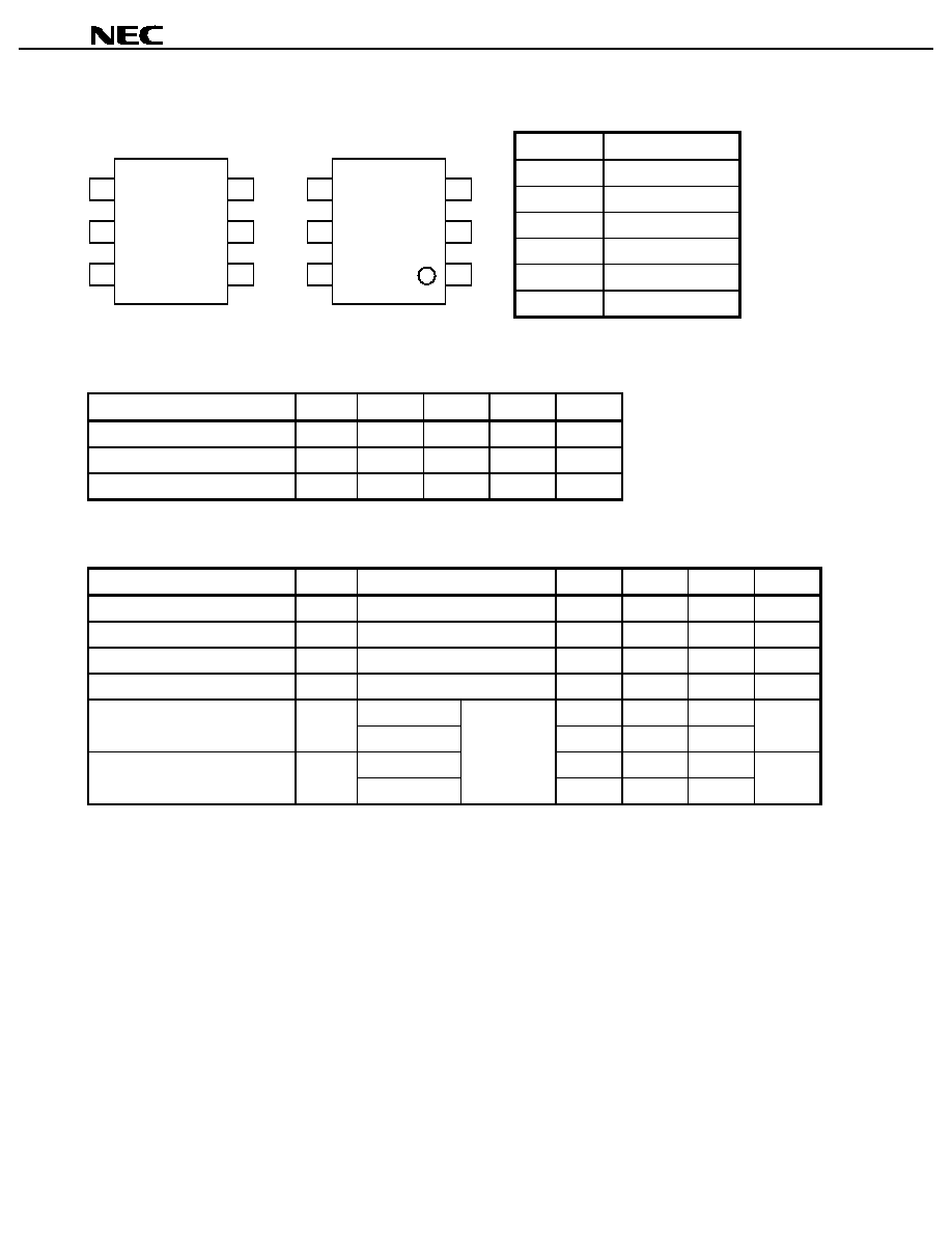
ORDERING INFORMATION
Part Number
Package
Marking
Supplying Form
NE429M01-T1
6-pin super minimold
V72
Embossed tape 8 mm wide.
1, 2, 3 pins face to perforation side of the tape
Qty 3 kpcs/reel
ABSOLUTE MAXIMUM RATINGS (T
A
= +25
∞
∞
∞
∞
C)
Parameter
Symbol
Ratings
Unit
Drain to Source Voltage
V
DS
4.0
V
Gate to Source Voltage
V
GS
-
3.0
V
Drain Current
I
D
I
DSS
mA
Gate Current
I
G
100
µ
A
Total Power Dissipation
P
tot
125
mW
Channel Temperature
T
ch
125
∞
C
Storage Temperature
T
stg
-
65 to +125
∞
C
Data Sheet P12254EJ3V0DS00
2
NE429M01
V
DS
= 2 V
I
D
= 10 mA
PIN CONNECTIONS
3
2
1
4
5
6
(Top View)
V72
4
5
6
3
2
1
(Bottom View)
RECOMMENDED OPERATING CONDITION (T
A
= +25
∞
C)
Parameter
Symbol
MIN.
TYP.
MAX.
Unit
Drain to Source Voltage
V
DS
1
2
3
V
Drain Current
I
D
5
10
20
mA
Input Power
P
in
-
-
0
dBm
ELECTRICAL CHARACTERISTICS (T
A
= +25
∞
∞
∞
∞
C)
Parameter
Symbol
Test Conditions
MIN.
TYP.
MAX.
Unit
Gate to Source Leak Current
I
GSO
V
GS
=
-
3 V
-
0.5
10
µ
A
Saturated Drain Current
I
DSS
V
DS
= 2 V, V
GS
= 0 V
20
60
90
mA
Gate to Source Cutoff Voltage
V
GS(off)
V
DS
= 2 V, I
D
= 100
µ
A
-
0.2
-
0.7
-
2.0
V
Transconductance
g
m
V
DS
= 2 V, I
D
= 10 mA
45
60
-
mS
Noise Figure
NF
f = 12 GHz
-
0.9
1.2
dB
f = 4 GHz
-
0.4
-
Associated Gain
G
a
f = 12 GHz
9.0
10
-
dB
f = 4 GHz
-
15.0
-
Pin No.
Pin name
1
Gate
2
Source
3
Source
4
Drain
5
Source
6
Source

Data Sheet P12254EJ3V0DS00
3
NE429M01
TYPICAL CHARACTERISTICS (T
A
= +25
∞
∞
∞
∞
C)
250
200
150
100
50
0
50
100
150
200
250
TOTAL POWER DISSIPATION vs.
AMBIENT TEMPERATURE
Ambient Temperature T
A
(∞C)
Total Power Dissipation P
tot
(mW)
60
40
20
0
≠2.0
≠1.0
0
DRAIN CURRENT vs.
GATE TO SOURCE VOLTAGE
Gate to Source Voltage V
GS
(V)
Drain Current I
D
(mA)
Frequency f (GHz)
Maximum Stable Gain MSG. (dB)
Maximum Available Gain MAG. (dB)
Forward Insertion Gain |S
21S
|
2
(dB)
V
DS
= 2 V
MAXIMUM AVAILABLE GAIN, FORWARD
INSERTION GAIN vs. FREQUENCY
24
20
16
12
8
4
1
30
2
4
20
6
8 10
14
V
DS
= 2 V
I
D
= 10 mA
MAG.
|S
21S
|
2
DRAIN CURRENT vs.
DRAIN TO SOURCE VOLTAGE
Drain to Source Voltage V
DS
(V)
100
80
60
40
20
0
5
1
Drain Current I
D
(mA)
V
GS
= 0 V
≠0.2 V
≠0.4 V
≠0.6 V
2
3
4
MSG.

Data Sheet P12254EJ3V0DS00
4
NE429M01
Gain Calculations
MSG. =
K =
MAG. = (K
±
K
2
-
1)
= S
11
∑ S
22
-
S
21
∑ S
12
Frequency f (GHz)
2.0
1.5
1.0
0.5
0
1
30
2
Noise Figure NF (dB)
V
DS
= 2 V
I
D
= 10 mA
4
20
6
8 10
14
20
16
12
8
4
0
Associated Gain G
a
(dB)
G
a
NF
NOISE FIGURE, ASSOCIATED GAIN vs.
FREQUENCY
1 +
2
-
S
11
2
-
S
22
2
2
S
12
S
21
S
21
S
12
S
21
S
12
