 | –≠–ª–µ–∫—Ç—Ä–æ–Ω–Ω—ã–π –∫–æ–º–ø–æ–Ω–µ–Ω—Ç: NE76038 | –°–∫–∞—á–∞—Ç—å:  PDF PDF  ZIP ZIP |
PART NUMBER
NE76038
PACKAGE OUTLINE
38
SYMBOLS
PARAMETERS AND CONDITIONS
UNITS
MIN
TYP
MAX
NF
OPT
1
Optimum Noise Figure at V
DS
= 3 V, I
DS
= 10 mA
f = 4 GHz
dB
0.8
1.2
f = 12 GHz
dB
1.8
G
A
Associated Gain at V
DS
= 3 V, I
DS
= 10 mA
f = 4 GHz
dB
12.0
13.0
f = 12 GHz
dB
7.5
I
DSS
Saturated Drain Current at V
DS
= 3 V, V
GS
= 0 V
mA
15
30
50
V
P
Pinch-off Voltage at V
DS
= 3 V, I
DS
= 0.1 mA
V
-3.0
-0.8
-0.5
g
m
Transconductance at V
DS
= 3 V, I
DS
= 10 mA
mS
30
40
70
I
GSO
Gate to Source Leakage Current at V
GS
= -3 V
µ
A
10
Note:
1. Typical values of noise figures are those obtained when 50% of the devices from a large number of lots were individually measured in a circuit
with the input individually tuned to obtain the minimum value. Maximum values are criteria established on the production line as a "go-no-go"
screening test with the fixture tuned for the "generic" type but not for each specimen.
NE76038
LOW NOISE
L TO Ku-BAND GaAs MESFET
FEATURES
∑
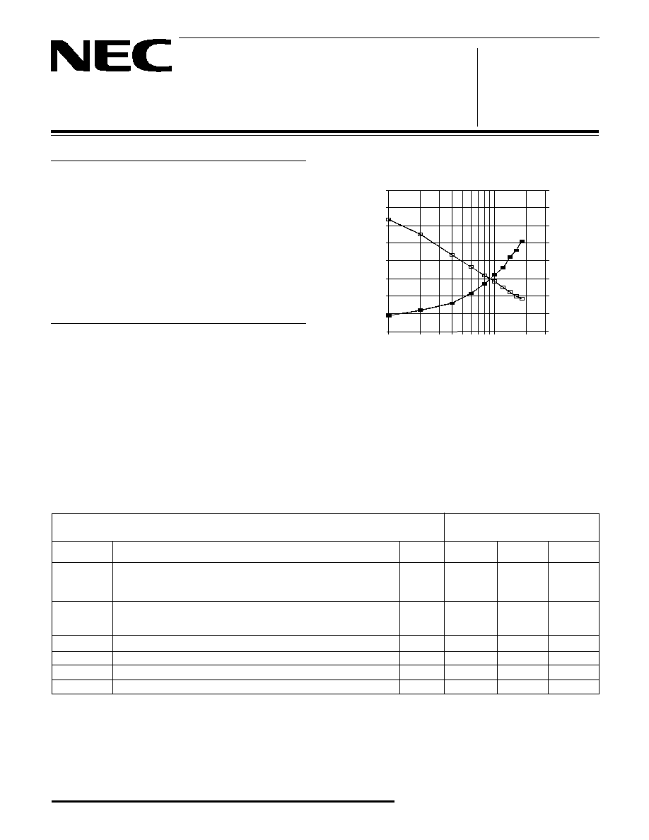
LOW NOISE FIGURE:
1.8 dB typical at 12 GHz
∑
HIGH ASSOCIATED GAIN:
7.5 dB typical at 12 GHz
∑
L
G
= 0.3
µ
m, W
G
= 280
µ
m
∑
LOW COST PLASTIC PACKAGING
∑
TAPE & REEL PACKAGING OPTION AVAILABLE
NOISE FIGURE & ASSOCIATED
GAIN vs. FREQUENCY
V
DS
= 3 V, I
DS
= 10 mA
Frequency, f (GHz)
Ga
NF
1 10 20
4
3.5
3
2.5
2
1.5
1
0.5
0
24
21
18
15
12
9
6
3
0
Noise Figure, NF (dB)
ELECTRICAL CHARACTERISTICS
(T
A
= 25
∞
C)
DESCRIPTION
NE76038 is a high performance gallium arsenide metal
semiconductor field effect transistor housed in a plastic
package. Its low noise figure makes this device appropriate
for use in the second or third stages of low noise amplifiers
operating in the 1 - 14 GHz frequency range. The device is
fabricated using ion implantation for improved RF and DC
performance, reliability, and uniformity. These devices fea-
ture a recessed 0.3 micron gate and triple epitaxial technol-
ogy.
NEC's stringent quality assurance and test procedures en-
sure the highest reliability and performance.
Associated Gain, G
A
(dB)
California Eastern Laboratories

SYMBOLS
PARAMETERS
UNITS
RATINGS
V
DS
Drain to Source Voltage
V
5
V
GD
Gate to Drain Voltage
V
-5
V
GS
Gate to Source Voltage
V
-3
I
DS
Drain Current
mA
I
DSS
P
IN
RF Input (CW)
dBm
+15
T
CH
Channel Temperature
∞
C
150
T
STG
Storage Temperature
∞
C
-65 to +150
P
T
Total Power Dissipation
mW
240
R
TH2, 3
Thermal Resistance
∞
C/W
1250
Notes:
1. Operation in excess of any one of these parameters may result in
permanent damage.
2. R
TH
for plastic package mounted on glass epoxy substrate is
965
∞
C/W.
3. R
TH
for chip mounted on copper heat sink is 190
∞
C/W.
NE76038
ABSOLUTE MAXIMUM RATINGS
1
(T
A
= 25
∞
C)
TYPICAL NOISE PARAMETERS
(T
A
= 25
∞
C)
FREQ.
NF
OPT
G
A
OPT
(GHz)
(dB)
(dB)
MAG
ANG
1
Rn/50
0.5
0.40
21.67
0.84
5
0.79
1.0
0.45
20.01
0.82
10
0.75
2.0
0.60
18.88
0.76
28
0.70
4.0
0.80
15.53
0.66
58
0.61
6.0
1.10
13.24
0.55
101
0.50
8.0
1.35
11.32
0.50
152
0.40
10.0
1.60
9.49
0.48
-166
0.31
12.0
1.80
8.15
0.54
-130
0.25
14.0
2.10
7.11
0.63
-105
0.20
16.0
2.30
6.54
0.70
-87
0.15
18.0
2.55
5.68
0.77
-75
0.12
V
DS
= 3 V, I
DS
= 10 mA
Note:
1.
OPT
is referenced to the bend of the lead, as shown on back page.
TOTAL POWER DISSIPATION vs.
AMBIENT TEMPERATURE
TYPICAL PERFORMANCE CURVES
(T
A
= 25
∞
C)
DRAIN CURRENT vs.
DRAIN TO SOURCE VOLTAGE
Ambient Temperature, T
A
(
∞
C)
Drain to Source Voltage, V
DS
(V)
Drain Current, I
DS
(mA)
Gate to Source Voltage, V
GS
(V)
Drain Current, I
DS
(mA)
DRAIN CURRENT vs.
GATE TO SOURCE VOLTAGE
V
DS
= 3 V
Total Power Dissipation, P
T
(mW)
-3 -2.5 -2 -1.5 -1 -0.5 0 0.5
35
30
25
20
15
10
5
0
0 25 50 75 100 125 150 175 200
300
250
200
150
100
50
0
Free Air
Infinite
Heat Sink
50
40
30
20
10
0
0 1 2 3 4 5
V
GS
= 0 V
-0.2 V
-0.4 V
-0.6 V

TYPICAL SCATTERING PARAMETERS
1
(T
A
= 25
∞
C)
FREQUENCY
S
11
S
21
S
12
S
22
K
MAG
2
(GHz)
MAG
ANG
MAG
ANG
MAG
ANG
MAG
ANG
(dB)
0.1
0.99
-2
3.29
178
0.006
101
0.63
-2
0.174
27.390
0.5
0.99
-9
3.29
171
0.013
82
0.63
-6
0.183
24.033
1.0
0.99
-17
3.25
163
0.02
78
0.62
-12
0.127
22.109
1.5
0.97
-25
3.25
155
0.03
71
0.61
-18
0.249
20.348
2.0
0.95
-34
3.22
147
0.04
66
0.60
-24
0.297
19.058
3.0
0.90
-51
3.15
131
0.06
57
0.58
-35
0.392
17.202
4.0
0.84
-68
3.07
115
0.08
47
0.54
-46
0.500
15.840
5.0
0.77
-86
2.97
99
0.09
37
0.50
-58
0.638
15.185
6.0
0.70
-106
2.83
84
0.10
28
0.45
-70
0.763
14.518
7.0
0.64
-126
2.66
69
0.11
21
0.41
-81
0.866
13.835
8.0
0.61
-145
2.51
55
0.11
16
0.37
-92
0.981
13.583
9.0
0.58
-165
2.37
42
0.11
10
0.33
-104
1.116
11.264
10.0
0.57
175
2.21
27
0.11
7
0.30
-118
1.228
10.152
11.0
0.58
156
2.05
15
0.12
3
0.27
-136
1.217
9.514
12.0
0.60
139
1.87
2
0.12
-0
0.27
-157
1.282
8.737
13.0
0.64
125
1.72
-10
0.12
-1
0.27
-178
1.301
8.274
14.0
0.67
114
1.57
-20
0.12
-2
0.30
164
1.325
7.756
15.0
0.71
104
1.45
-32
0.13
-4
0.34
150
1.175
7.941
16.0
0.74
95
1.32
-41
0.13
-8
0.39
135
1.158
7.653
17.0
0.77
86
1.19
-52
0.13
-12
0.44
122
1.127
7.453
18.0
0.78
80
1.09
-61
0.14
-17
0.46
111
1.094
7.043
V
DS
= 3 V, I
DS
= 30 mA
0.1
0.99
-2
4.36
178
0.004
94
0.57
-2
0.335
30.374
0.5
0.99
-10
4.36
171
0.011
82
0.57
-6
0.174
25.981
1.0
0.98
-19
4.30
161
0.02
78
0.57
-12
0.198
23.324
1.5
0.96
-28
4.27
153
0.03
72
0.56
-18
0.265
21.533
2.0
0.93
-37
4.19
144
0.04
67
0.55
-24
0.347
20.202
3.0
0.86
-56
4.02
127
0.05
58
0.52
-35
0.526
19.053
4.0
0.79
-74
3.83
111
0.07
49
0.48
-45
0.614
17.381
5.0
0.71
-93
3.62
95
0.08
41
0.44
-56
0.754
16.556
6.0
0.64
-114
3.37
80
0.08
35
0.39
-67
0.954
16.245
7.0
0.58
-134
3.13
66
0.09
29
0.35
-78
1.052
14.015
8.0
0.55
-154
2.91
52
0.09
26
0.32
-88
1.191
12.451
9.0
0.53
-173
2.71
39
0.10
22
0.29
-100
1.213
11.546
10.0
0.53
167
2.51
26
0.10
20
0.26
-114
1.324
10.587
11.0
0.55
149
2.31
14
0.11
16
0.23
-132
1.304
9.918
12.0
0.58
133
2.11
1
0.11
13
0.23
-155
1.362
9.237
13.0
0.63
120
1.94
-9
0.12
10
0.24
-178
1.259
9.023
14.0
0.66
110
1.77
-20
0.13
8
0.27
163
1.206
8.599
15.0
0.70
101
1.65
-31
0.14
3
0.31
149
1.083
8.955
16.0
0.73
92
1.50
-41
0.14
-2
0.36
134
1.078
8.600
17.0
0.76
84
1.35
-51
0.15
-7
0.41
121
1.007
9.034
18.0
0.78
78
1.23
-59
0.15
-12
0.45
110
1.006
8.680
V
DS
= 3 V, l
D
s = 10 mA
Note:
1. S-Parameters are de-embedded to the bend of the lead as shown on back page.
2. Gain calculations:
MAG =
|S
21
|
|S
12
|
K - 1
).
2
(
K
±
= S
11
S
22
- S
21
S
12
When K
1, MAG is undefined and MSG values are used. MSG =
|S
21
|
|S
12
|
, K = 1 + |
| - |S
11
| - |S
22
|
2
2
2
2 |S
12
S
21
|
,
MAG = Maximum Available Gain
MSG = Maximum Stable Gain
NE76038

NE76038
Parameter
Units
capacitance
picofarads
inductance
nanohenries
resistance
ohms
Parameters
Q1
Parameters
Q1
VTO
-0.73
RG
0
VTOSC
0
RD
0
ALPHA
4
RS
0
BETA
0.063
RGMET
0
GAMMA
0
KF
0
GAMMADC
(2)
0.06
AF
1
Q
2.2
TNOM
27
DELTA
0.7
XTI
3
VBI
0.626
EG
1.43
IS
1.98e-11
VTOTC
0
N
1.4
BETATCE
0
RIS
0
FFE
1
RID
0
TAU
3.2e-12
CDS
0.11e-12
RDB
Infinity
CBS
0
CGSO
(3)
0.4e-12
CGDO
(4)
0.04e-12
DELTA
1
0.3
DELTA
2
0.2
FC
0.5
VBR
Infinity
NE76038 NONLINEAR MODEL
FET NONLINEAR MODEL PARAMETERS
(1)
UNITS
MODEL RANGE
Frequency:
0.1 to 18 GHz
Bias:
V
DS
= 3 V, I
D
= 10 mA to 30 mA
Date:
8/30/96
(1) Series IV Libra TOM Model
The parameter in Libra corresponds to the parameter in PSpice:
(2) GAMMADC
GAMMA
(3) CGSO
CGS
(4) CGDO
CGD
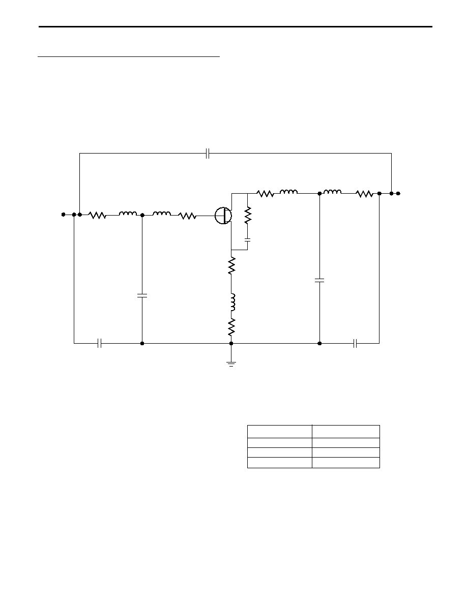
NE76038
CGD_PKG
0.01
DRAIN
RD_PKG
LD_PKG
R_COMP
365
CRF_X
500
LS_PKG
0.18
RS_PKG
0.1
CSD_PKG
CCD_PKG
0.06
CCG_PKG
0.06
CSG_PKG
0.003
0.02
SOURCE
0.38
0.53
0.06
2
LD
RD
RS
4.6
76000
RG
LG
LG_PKG
RG_PKG
GATE
1.3
0.64
0.14
1.5
Parameter
Units
capacitance
picofarads
inductance
nanohenries
resistance
ohms
SCHEMATIC
UNITS
MODEL RANGE
Frequency:
0.1 to 18 GHz
Bias:
V
DS
= 3 V, I
D
= 10 mA to 30 mA
Date:
8/30/96
NE76038 NONLINEAR MODEL
OUTLINE DIMENSIONS
(Units in mm)
1.8
±
0.2
1.8
±
0.2
S
G
D
S
GATE LEAD MARK
0.5
±
0.1
ALL LEADS
4∞
0.55
±
0.1
1.1
±
0.1
0.1
+0.2
-0.1
0.5 MIN
8 ∞
0.12
±
0.05
3∞
1.8
±
0.2
4.0
±
0.2
PACKAGE OUTLINE 38
PART
AVAILABILITY
PACKAGE
NUMBER
OUTLINE
NE76038
Bulk up to 1 K
38
NE76038-T1
1K/Reel
38
ORDERING INFORMATION
NE76038
EXCLUSIVE NORTH AMERICAN AGENT FOR RF, MICROWAVE & OPTOELECTRONIC SEMICONDUCTORS
CALIFORNIA EASTERN LABORATORIES ∑ Headquarters ∑ 4590 Patrick Henry Drive ∑ Santa Clara, CA 95054-1817 ∑ (408) 988-3500 ∑ Telex 34-6393 ∑ FAX (408) 988-0279
24-Hour Fax-On-Demand: 800-390-3232 (U.S. and Canada only) ∑ Internet: http://WWW.CEL.COM
PRINTED IN USA ON RECYCLED PAPER -8/98
DATA SUBJECT TO CHANGE WITHOUT NOTICE