 | –≠–ª–µ–∫—Ç—Ä–æ–Ω–Ω—ã–π –∫–æ–º–ø–æ–Ω–µ–Ω—Ç: NE894M13 | –°–∫–∞—á–∞—Ç—å:  PDF PDF  ZIP ZIP |

NE894M13
NPN SILICON TRANSISTOR
∑
NEW MINIATURE M13 PACKAGE:
≠ Small transistor outline
≠ 1.0 X 0.5 X 0.5 mm
≠ Low profile / 0.50 mm package height
≠ Flat lead style for better RF performance
∑
IDEAL FOR > 3 GHz OSCILLATORS
∑
LOW NOISE, HIGH GAIN
∑
LOW C
re
∑
UHSO 25 GHz PROCESS
FEATURES
OUTLINE DIMENSIONS
(Units in mm)
PACKAGE OUTLINE M13
PART NUMBER
NE894M13
EIAJ
1
REGISTERED NUMBER
2SC5787
PACKAGE OUTLINE
M13
SYMBOLS
PARAMETERS AND CONDITIONS
UNITS
MIN
TYP
MAX
f
T
Gain Bandwidth at V
CE
= 1 V, I
C
= 20 mA, f = 2 GHz
GHz
17
20
≠
|S
21E
|
2
Insertion Power Gain at V
CE
= 1 V, I
C
= 20 mA, f = 2 GHz
dB
11
13
≠
|
NF
Noise Figure at V
CE
= 1 V, I
C
= 5 mA, f = 2 GHz, Z
S
= Z
OPT
dB
≠
1.4
2.5
C
re
Reverse Transfer Capacitance
3
at V
CB
= 0.5 V, I
E
= 0 mA, f = 1 MHz
pF
≠
0.22
0.30
I
CBO
Collector Cutoff Current at V
CB
= 5 V, I
E
= 0
nA
≠
≠
100
I
EBO
Emitter Cutoff Current at V
EB
= 1 V, I
C
= 0
nA
≠
≠
100
h
FE
DC Current Gain
2
at V
CE
= 1 V, I
C
= 5 mA
50
≠
100
ELECTRICAL CHARACTERISTICS
(T
A
= 25
∞
C)
Notes:
1. Electronic Industrial Association of Japan.
2. Pulsed measurement, pulse width
350
µ
s, duty cycle
2 %.
3. Collector to base capacitance when the emitter is grounded
DESCRIPTION
The NE894M13 transistor is designed for oscillator applica-
tions above 3 GHz. The NE894M13 features low voltage, low
current operation, low noise, and high gain. NEC's new low
profile/flat lead style "M13" package is ideal for today's portable
wireless applications.
California Eastern Laboratories
1. Emitter
2. Base
3. Collector
PIN CONNECTIONS
0.125
+0.1 Ò0.05
0.5±0.05
0.1
0.1
0.2
+0.1 Ò0.05
0.35
0.7
0.35
0.15
+0.1 Ò0.05
0.15
+0.1 Ò0.05
1.0
+0.1 Ò0.05
0.5
+0.1
Ò0.05
0.7±0.05
1
2
3
B7
0.3
0.2
0.2
(Bottom View)
Notes:
1. Operation in excess of any one of these parameters may result
in permanent damage.
2. With device mounted on 1.08 cm
2
X 1.0 mm glass epoxy board.
SYMBOLS
PARAMETERS
UNITS
RATINGS
V
CBO
Collector to Base Voltage
V
9
V
CEO
Collector to Emitter Voltage
V
3.0
V
EBO
Emitter to Base Voltage
V
1.5
I
C
Collector Current
mA
35
P
T2
Total Power Dissipation
mW
105
T
J
Junction Temperature
∞
C
150
T
STG
Storage Temperature
∞
C
-65 to +150
ABSOLUTE MAXIMUM RATINGS
1
(T
A
= 25
∞
C)
Ambient Temperature, T
A
(
∞
C)
Total Power Dissipation, P
tot
(mW)
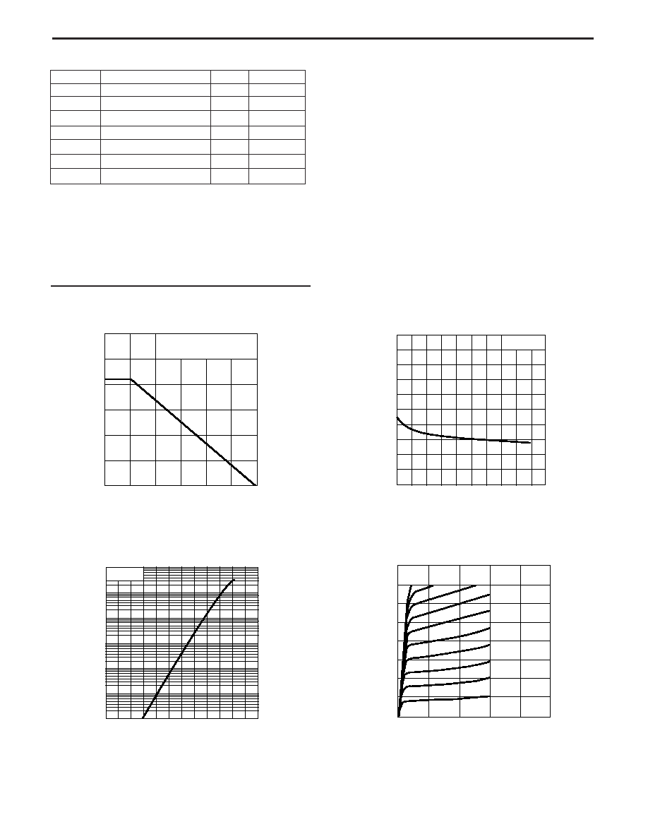
TOTAL POWER DISSIPATION vs.
AMBIENT TEMPERATURE
TYPICAL PERFORMANCE CURVES
(T
A
= 25
∞
C)
Collector to Base Voltage, V
CB
(V)
Reverse Transfer Capacitance, C
re
(pF)
REVERSE TRANSFR CAPACITANCE vs.
COLLECTOR TO BASE VOLTAGE
150
125
100
75
50
25
0
105
Mounted on Glass epoxy PCB
(1.08 cm
2
x 1.0 mm (t) )
0
25
50
75
100
125
150
0.5
0.4
0.3
0.2
0.1
0
0
2
4
6
8
10
f = 1 MHz
NE894M13
V
CE
= 1 V
100
10
1
0.1
0.001
0.0001
0.01
0.4
0.5
0.6
0.7
0.8
0.9
1.0
Base to Emitter Voltage, V
BE
(V)
Collector Current, I
C
(mA)
COLLECTOR CURRENT vs.
BASE TO EMITTER VOLTAGE
40
30
20
10
0
0
1
2
3
4
5
500
µ
A
150
µ
A
200
µ
A
250
µ
A
300
µ
A
350
µ
A
400
µ
A
450
µ
A
100
µ
A
I
B
= 500
µ
A
Collector Current, I
C
(mA)
COLLECTOR CURRENT vs.
COLLECTOR TO EMITTER VOLTAGE
Collector to Emitter Voltage, V
CE
(V)

TYPICAL PERFORMANCE CURVES
(T
A
= 25
∞
C)
28
24
20
16
12
8
4
0
1
10
100
V
CE
= 1 V
f = 2 GHz
40
35
30
25
20
15
10
5
0
0.1
1
10
MSG
MAG
|S
21e
|
2
V
CE
= 1 V
I
C
= 20 mA
20
16
12
8
4
0
1
10
MSG
MAG
|S
21e
|
2
100
V
CE
= 2 V
f = 2 GHz
20
16
12
8
4
0
1
10
MSG
MAG
|S
21e
|
2
100
V
CE
= 2 V
f = 2 GHz
Collector Current, I
C
(mA)
NE894M13
20
16
12
8
4
0
1
10
100
V
CE
= 1 V
f = 4 GHz
MSG
MAG
|S
21e
|
2
20
16
12
8
4
0
1
10
100
V
CE
= 2 V
f = 4 GHz
MSG
MAG
|S
21e
|
2
Insertion Power Gain, |S
21e
|
2
(dB)
Maximum Available Gain, MAG(dB)
Maximum Stable Gain, MSG(dB)
INSERTION POWER GAIN, MAG, MSG
vs. FREQUENCY
Collector Current, I
C
(mA)
INSERTION POWER GAIN, MAG, MSG
vs. COLLECTOR CURRENT
Associated Gain, G
a
(dB)
Collector Current, I
C
(mA)
Collector Current, I
C
(mA)
Gain Bandwidth Product, f
T
(GHz)
Collector Current, I
C
(mA)
GAIN BANDWIDTH PRODUCT
vs. COLLECTOR CURRENT
Frequency, f (GHz)
Insertion Power Gain, |S
21e
|
2
(dB)
Maximum Available Gain, MAG(dB)
Maximum Stable Gain, MSG(dB)
INSERTION POWER GAIN, MAG, MSG
vs. COLLECTOR CURRENT
Insertion Power Gain, |S
21e
|
2
(dB)
Maximum Available Gain, MAG(dB)
Maximum Stable Gain, MSG(dB)
INSERTION POWER GAIN, MAG, MSG
vs. COLLECTOR CURRENT
Insertion Power Gain, |S
21e
|
2
(dB)
Maximum Available Gain, MAG(dB)
Maximum Stable Gain, MSG(dB)
INSERTION POWER GAIN, MAG, MSG
vs. COLLECTOR CURRENT
Insertion Power Gain, |S
21e
|
2
(dB)
Maximum Available Gain, MAG(dB)
Maximum Stable Gain, MSG(dB)
NE894M13
5
4
3
2
1
0
1
10
100
0
4
8
12
16
20
V
CE
= 1 V
f = 1 GHz
Ga
NF
Noise Figure, NF (dB)
NOISE FIGURE, ASSOCIATED GAIN
vs. COLLECTOR CURRENT
TYPICAL PERFORMANCE CURVES
(T
A
= 25
∞
C)
Associated Gain, G
a
(dB)
Collector Current, I
C
(mA)
5
4
3
2
1
0
1
10
100
0
4
8
12
16
20
V
CE
= 1 V
f = 2 GHz
Ga
NF
Collector Current, I
C
(mA)
Associated Gain, G
a
(dB)
Noise Figure, NF (dB)
NOISE FIGURE, ASSOCIATED GAIN
vs. COLLECTOR CURRENT
NE894M13
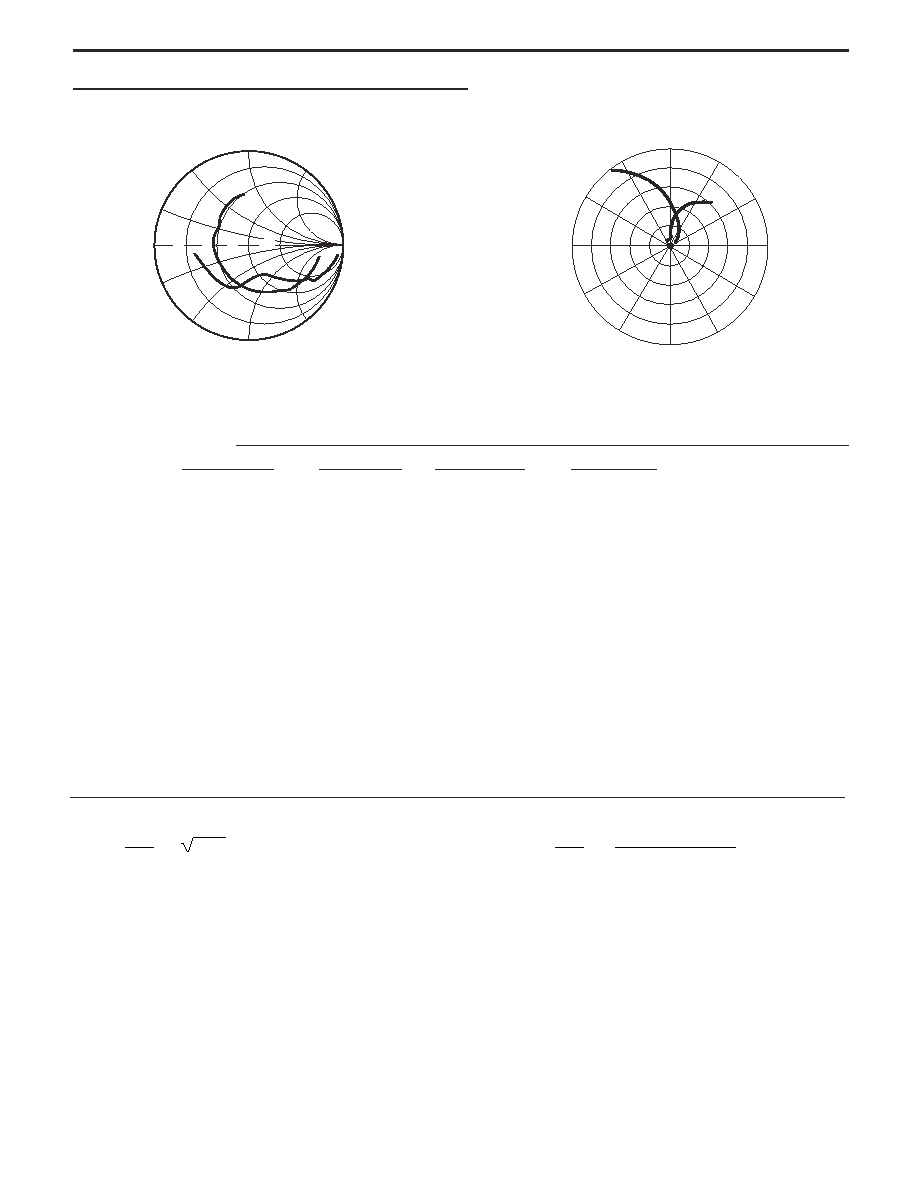
TYPICAL SCATTERING PARAMETERS
(T
A
= 25
∞
C)
Note:
1. Gain Calculations:
MAG =
|S
21
|
|S
12
|
K - 1
).
2
(
K
±
= S
11
S
22
- S
21
S
12
When K
1, MAG is undefined and MSG values are used. MSG =
|S
21
|
|S
12
|
, K = 1 + |
| - |S
11
| - |S
22
|
2
2
2
2 |S
12
S
21
|
,
MAG = Maximum Available Gain
MSG = Maximum Stable Gain
FREQUENCY
S
11
S
21
S
12
S
22
K
MAG
1
GHz
MAG
ANG
MAG
ANG
MAG
ANG
MAG
ANG
(dB)
NE894M13
V
C
= 1 V, I
C
= 5 mA
0.10
0.772
- 11.0
13.002
169.8
0.011
85.6
0.966
- 8.4
0.10
30.55
0.20
0.747
- 24.6
12.548
159.5
0.022
76.8
0.928
- 15.8
0.17
27.54
0.30
0.715
- 36.5
11.948
150.4
0.032
70.6
0.883
- 22.5
0.22
25.75
0.40
0.677
- 47.7
11.241
142.4
0.040
66.2
0.835
- 28.3
0.27
24.50
0.50
0.612
- 59.5
10.457
134.1
0.046
61.3
0.758
- 31.4
0.39
23.57
0.60
0.575
- 68.8
9.699
127.9
0.051
58.2
0.707
- 35.7
0.44
22.79
0.70
0.544
- 76.9
8.993
122.5
0.056
56.5
0.658
- 39.1
0.50
22.09
0.80
0.517
- 84.6
8.364
117.7
0.059
54.9
0.623
- 41.6
0.54
21.50
0.90
0.493
- 91.3
7.756
113.5
0.062
54.1
0.590
- 44.1
0.59
20.94
1.00
0.474
- 97.3
7.228
109.6
0.065
53.6
0.558
- 45.9
0.65
20.46
2.00
0.383
-135.0
4.155
84.4
0.088
58.8
0.411
- 59.5
1.01
16.27
3.00
0.362
-155.9
2.920
68.1
0.120
67.4
0.383
- 73.2
1.10
11.97
4.00
0.355
-175.7
2.253
54.6
0.162
72.0
0.412
- 88.5
1.05
10.08
5.00
0.352
169.2
1.821
44.0
0.215
73.4
0.476
- 98.4
0.95
9.28
6.00
0.339
158.2
1.561
36.0
0.281
72.6
0.512
-103.6
0.86
7.44
7.00
0.359
145.9
1.390
28.0
0.358
68.5
0.522
-114.0
0.81
5.89
8.00
0.394
132.7
1.251
20.9
0.438
62.5
0.523
-127.0
0.79
4.56
9.00
0.432
121.6
1.137
14.9
0.513
55.6
0.521
-142.1
0.80
3.45
10.00
0.466
110.0
1.026
10.5
0.569
48.7
0.543
-157.6
0.84
2.56
11.00
0.489
99.5
0.930
8.9
0.609
43.9
0.572
-165.7
0.87
1.84
12.00
0.489
92.9
0.878
9.3
0.653
40.4
0.567
-168.8
0.90
1.28
0.100 to 12.000 GHz by 0.050
j50
j25
j10
10
25
-j10
-j25
-j50
-j100
j100
0
50
100
0
S
11
S
22
0.100 to 12.000GHz by 0.050
120∞
90∞
60∞
30∞
150∞
180∞
-150∞
-120∞
-90∞
-60∞
-30∞
0∞
S
12
S
21