NEC's 1550 nm
InGaAsP MQW DFB LASER DIODE
IN COAXIAL PACKAGE
FOR 155 Mb/s AND 622 Mb/s APPLICATIONS
NX8503BG-CC
NX8503CG-CC
FEATURES
∑ PEAK EMISSION WAVELENGTH:
P
= 1550 nm
∑ OPTICAL OUTPUT POWER:
P
f
= 2.0 mW
∑ LOW THRESHOLD CURRENT:
I
TH
= 15 mA @ T
C
= 25
∞
C
∑ InGaAs MONITOR PIN-PD
∑ WIDE OPERATING TEMPERATURE RANGE:
T
C
= -10 to +85
∞
C
∑ WITH SC-UPC CONNECTOR
∑ BASED ON TELCORDIA RELIABILITY
NEC's NX8503BG-CC and NX8503CG-CC are 1550 nm Co-
axial Module DFB (Distributed Feed-Back) laser diode with
single mode fiber. Multiple Quantum Well (MQW) structure is
adopted to achieve stable dynamic single longitudinal mode
operation over a wide temperature range of -10 to +85
∞
C.
The module is ideal as a light source for Synchronous Digital
Hierarchy (SDH) system, STM-1, log-haul L-1.2, L-1.3 and
STM-4, long-haul L-4.2, L-4.3 ITU-T recommendations.
DESCRIPTION
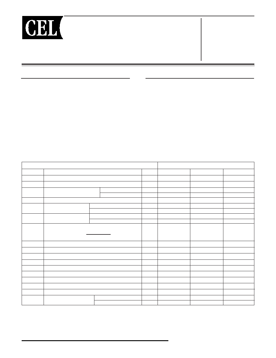
PART NUMBER
NX8300BG-CC, NX8300CG-CC
SYMBOLS
PARAMETERS AND CONDITIONS
UNITS
MIN
TYP
MAX
P
f
Optical Output Power from Fiber, CW
mW
2.0
V
OP
Operating Voltage,
P
f
= 2.0 mW
V
1.1
1.6
I
TH
Threshold Current
T
C
= +25
∞
C
mA
15
25
mA
2
50
P
TH
Threshold Output Power, I
F
= I
TH
µ
W
100
I
MOD
Modulation Current
P
f
= 2.0 mW, T
C
= 25
∞
C
mA
15
25
40
P
f
= 2.0 mW
mA
13
60
d
Differential Efficiency
P
f
= 2.0 mW, T
C
= 25
∞
C
W/A
0.050
0.080
0.130
P
f
= 2.0 mW
W/A
0.030
0.150
d
Temperature Dependence of Differential Efficiency,
dB
-3
-1.6
Kink
Kink, P
f
= Up to 2.4 mW (Refer to defenitions)
%
±
20
p
Peak Emission Wavelength, P
f
= 2.0 mW
nm
1530
1550
1570
/
T
Temperature Dependence of Peak Emission Wavelength
nm/
∞
C
0.1
0.12
Spectral Width, P
f
= 2.0 mW, -20 dB down width
nm
0.3
1.0
SMSR
Side Mode Suppression Ratio, P
f
= 2.0 mW
dB
30
40
f
c
Cut-off Frequency, -3 dB, V
R
= 5 V, P
f
= 2.0 mW
GHz
2.0
t
r
Rise Time, 10 to 90%, P
pk
= 2.0 mW, I
F
= I
TH
ns
0.5
t
f
Fall Time, 90 to 10%, P
pk
= 2.0 mW, I
F
= I
TH
ns
0.5
I
m
Monitor Current, V
R
= 5 V, P
f
= 2.0 mW
µ
A
200
1000
2000
I
D
Monitor Dark Current
V
R
= 5 V, T
C
= 25
∞
C
nA
1.0
50
V
R
= 5 V
nA
10
500
ELECTRO-OPTICAL CHARACTERISTICS
(T
C
= -10 to +85
∞
C, unless otherwise specified)
d
= 10 log
d
(@ T
C
∞C)
d
(@ 25 ∞C)
continued next page
California Eastern Laboratories
ABSOLUTE MAXIMUM RATINGS
1
(T
C
= -20 to +85
∞
C, unless otherwise specified)
SYMBOLS
PARAMETERS
UNITS
RATINGS
I
F
Forward Current of LD
mA
150
P
f
Optical Output Power
mW
5.0
from Fiber
V
R
Reverse Voltage of LD
V
2.0
I
F
Forward Current of PD
mA
2.0
V
R
Reverse Voltage of PD
V
15
T
C
Operating Case Temperature
∞
C
-10 to +85
T
STG
Storage Temperature
∞
C
-40 to +85
T
SLD
Lead Soldering
Temperature (10 s)
∞
C
260
RH
Relative Humidity
%
85
(non-condensing)
Note:
1. Operation in excess of any one of these parameters may result
in permanent damage.
NX8503BG-CC, NX8503CG-CC
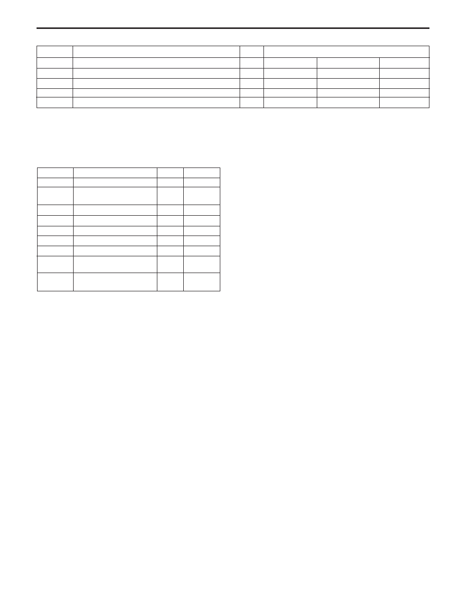
PART NUMBER
NX8503BG-CC, NX8503BG-CC
SYMBOLS
PARAMETERS AND CONDITIONS
UNITS
MIN
TYP
MAX
C
t
Monitor PD Terminal Capacitance, V
R
= 5 V, f = 1 MHz
pF
1.0
20
LIN
m
Linearity, V
R
= 5 V, P
f
= 0.2 to 2.0 mW (Refer to defenitions)
%
10
Tracking Error, I
m
= const. (Refer to defenitions)
dB
0.5
1.0
RIN
Relative Intensity Noise, Ref = -14dB
dB/Hz
-135
ELECTRO-OPTICAL CHARACTERISTICS
cont.
(T
C
= -10 to +85
∞
C, unless otherwise specified)

NX8503BG-CC, NX8503CG-CC
TYPICAL CHARACTERISTICS
(TC = 25 ∫C, Unless otherwise specified)
Case Temperature Tc (∫C)
Peak Emission Wavelenght
p
(nm)
1565
1560
1555
1550
1545
-40
-20
0
20
40
60
80
100
TEMPERATURE DEPENEDENCE OF
DIFFERNTIAL EFFICIENCY
Case Temperature Tc (∫C)
Differemtial Effieciency
d
(W/A)
0.06
0.00
-40
-20
0
0.18
0.12
20
40
60
80
100
TEMPERATURE DEPENEDENCE OF
PEAK EMISSION WAVELENGHT
OPERATING CURRENT AND THRESHOLD CURRENT
vs. CASE TEMPERATURE
Case Temperature T
c
(∫C)
Operating Current I
op
(mA)
Threshold Curent I
th
(mA)
Forward Voltage V
F
(V)
Forward Current I
F
(mA)
100
10
1
-40
-20
0
20
40
60
80
100
I
th
I
op
@
P
r
= 2 mW
0
10
0.5
1.0
1.5
2.0
2.5
20
30
40
50
FORWARD CURRENT vs.
FORWARD VOLTAGE
SPECTRUM
Wavelength
(nm)
Relative Intensity (dB)
1565.0
1555.0
1545.0
10
0
-10
-20
-30
-40
-50
-60
-70
REMARK The graphs indicate nominal charachteristics.

PART NUMBER AVAILABLE CONNECTOR
FLANGE TYPE
NX8503BG-CC
With SC-UPC Connector
NX8503CG-CC
ORDERING INFORMATION
Flat Mount Flange
PARAMETER
SPEC
UNIT
Mode Field Doameter
9.5
±
1
µ
m
Cladding Diameter
125
±
2
µ
m
Maximum Cladding Noncircularity
2
%
Maximum Core/Cladding Concentricity
1.6
%
Outer Diameter
0.9
±
0.1
mm
Cut-off Wavelength
1100 to 1270
nm
Minimum Fiber Bending Radius
30
mm
Fiber Length
500
±
50 MIN
mm
Flammability
UL1581 VW-1
OPTICAL FIBER CHARACTERISTICS
35±2 mm
Fiber Length: 500±50 mm
SC-UPC Connector
8.99±0.5 mm
OUTLINE DIMENSIONS
(Units in mm)
¯0.9
Optical Fiber (SMF)
Length: 0.5 m
With SC Connector
8.0±0.3
¯7.0±0.2
4.0±0.2
2.2
3.2
¯2.2
¯0.45±0.05
18.3±1.0
25.5±1.0
1.2±0.2
20.0±1.0
12.7±0.2
17.0±0.2
P.C.D. = ¯2.0
7.2±0.3
3.7±0.3
1.0±0.1
PD
LD
4
1
3
2
CASE
6.0
¯0.9
Optical Fiber (SMF)
Length: 0.5 m
With SC Connector
8.0±0.3
0.5±0.3
¯7.0±0.2
¯0.45±0.05
15.0
7.3
0.5
28.3±1.0
19.5±1.0
16.0
6.0
PD
3
2
LD
4
1
CASE
P.C.D. = ¯2.0
4≠R1.25±0.2
2≠¯2.5
8.5±0.2
1
2
3
4
12.0±0.15
7.0±0.2
NX8503BG-CC, NX8503CG-CC
Vertical Mount
Flange
NX8503BG-CC
NX8503CG-CC
PIN CONNECTIONS
PIN CONNECTIONS
Life Support Applications
These NEC products are not intended for use in life support devices, appliances, or systems where the malfunction of these products can reasonably be expected
to result in personal injury. The customers of CEL using or selling these products for use in such applications do so at their own risk and agree to fully indemnify
CEL for all damages resulting from such improper use or sale.
A Business Partner of NEC Compound Semiconductor Devices, Ltd.
03/03/2003
