 | –≠–ª–µ–∫—Ç—Ä–æ–Ω–Ω—ã–π –∫–æ–º–ø–æ–Ω–µ–Ω—Ç: RD6.8S | –°–∫–∞—á–∞—Ç—å:  PDF PDF  ZIP ZIP |
©
1995
DATA SHEET
ZENER DIODES
RD2.0S to RD120S
DESCRIPTION
Type RD2.0S to RD120S Series are 2 PIN Super Mini
Mold Package zener diodes possessing an allowable power
dissipation of 200 mW.
FEATURES
∑
Sharp Breakdown characteristic.
∑
Vz: Applied E24 standard.
APPLICATIONS
Circuit for Constant Voltage, Constant Current, Wave form
Clipper, Surge absorber, etc.
Document No. D11444EJ3V0DS00 (3rd edition)
Date Published March 1999 N CP(K)
Printed in Japan
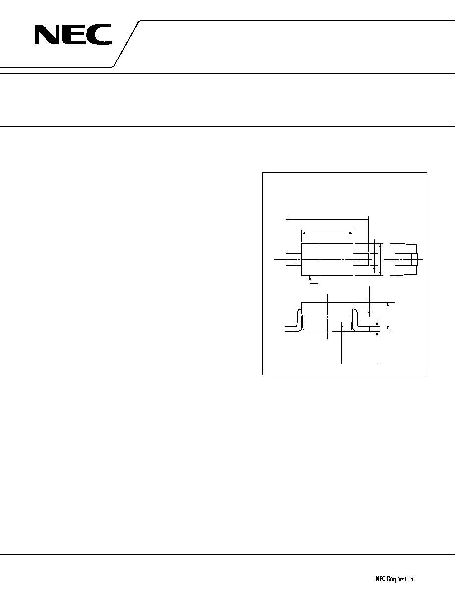
PACKAGE DIMENSIONS
(in millimeter)
ZENER DIODES
200 mW 2 PINS SUPER MINI MOLD
,,
,,,
,
2.5±0.15
0.11
+0.05 ≠0.01
1.7±0.1
0.3±0.05
1.25±0.1
Cathode
Indication
0.9±0.1
0.19
0±0.05
(in millimeters)
PACKAGE DIMENSIONS
ABSOLUTE MAXIMUM RATINGS (T
A
= 25
∞
C)
Power Dissipation
P
200 mW
Forward Current
I
F
100 mA
Reverse Surge Power
P
RSM
85 W (at t=10
µ
s/1 pulse) Show Fig. 12
Junction Temperature
T
j
150
∞
C
Storage Temperature
T
stg
≠55 to +150
∞
C
The information in this document is subject to change without notice. Before using this document, please
confirm that this is the latest version.
Not all devices/types available in every country. Please check with local NEC representative for availability
and additional information.
RD2.0S to RD120S
2
Data Sheet D11444EJ3V0DS00
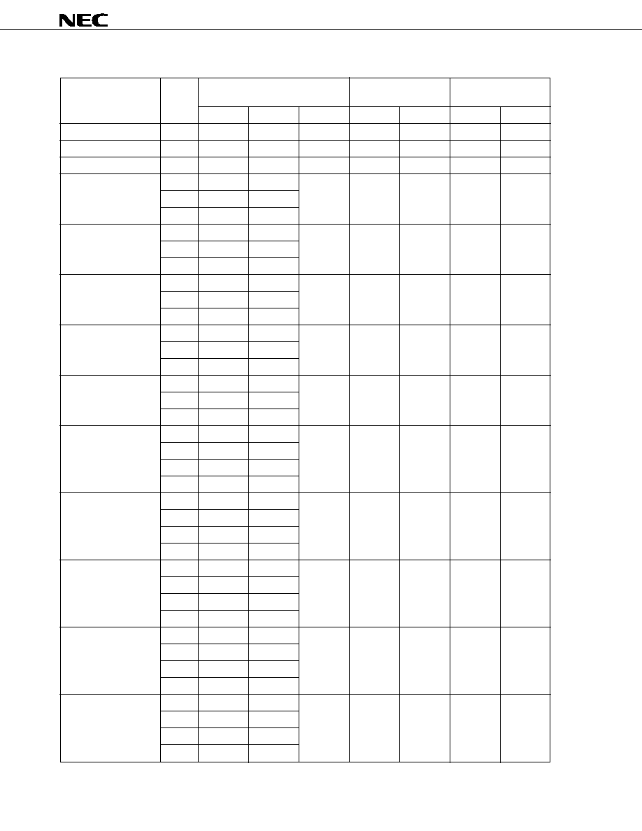
ELECTRICAL CHARACTERISTICS (T
A
= 25
±
2
∞
C)
Type Number
Class
Zener Voltage
Dynamic
Reverse Current
Vz (V)
Note 1
Impedance Zz (
)
Note 2
I
R
(
µ
A)
MIN.
MAX.
Iz (mA)
MAX.
Iz (mA)
MAX.
V
R
(V)
RD2.0S
B
1.90
2.20
5
100
5
120
0.5
RD2.2S
B
2.10
2.40
5
100
5
120
0.7
RD2.4S
B
2.30
2.60
5
100
5
120
1.0
RD2.7S
B
2.50
2.90
5
110
5
120
1.0
B1
2.50
2.75
B2
2.65
2.90
RD3.0S
B
2.80
3.20
5
120
5
50
1.0
B1
2.80
3.05
B2
2.95
3.20
RD3.3S
B
3.10
3.50
5
130
5
20
1.0
B1
3.10
3.35
B2
3.25
3.50
RD3.6S
B
3.40
3.80
5
130
5
10
1.0
B1
3.40
3.65
B2
3.55
3.80
RD3.9S
B
3.70
4.10
5
130
5
10
1.0
B1
3.70
3.97
B2
3.87
4.10
RD4.3S
B
4.00
4.49
5
130
5
10
1.0
B1
4.00
4.22
B2
4.14
4.35
B3
4.27
4.49
RD4.7S
B
4.40
4.92
5
130
5
10
1.0
B1
4.40
4.63
B2
4.53
4.77
B3
4.67
4.92
RD5.1S
B
4.82
5.39
5
130
5
5
1.5
B1
4.82
5.06
B2
4.96
5.22
B3
5.12
5.39
RD5.6S
B
5.29
5.94
5
80
5
5
2.5
B1
5.29
5.57
B2
5.47
5.75
B3
5.65
5.94
RD6.2S
B
5.84
6.55
5
50
5
2
3.0
B1
5.84
6.14
B2
6.04
6.35
B3
6.24
6.55
RD2.0S to RD120S
3
Data Sheet D11444EJ3V0DS00
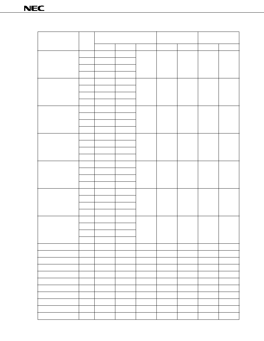
ELECTRICAL CHARACTERISTICS (T
A
= 25
±
2
∞
C)
Type Number
Class
Zener Voltage
Dynamic
Reverse Current
Vz (V)
Note 1
Impedance Zz (
)
Note 2
I
R
(
µ
A)
MIN.
MAX.
Iz (mA)
MAX.
Iz (mA)
MAX.
V
R
(V)
RD6.8S
B
6.44
7.17
5
30
5
2
3.5
B1
6.44
6.76
B2
6.62
6.96
B3
6.83
7.17
RD7.5S
B
7.03
7.87
5
30
5
2
4.0
B1
7.03
7.39
B2
7.25
7.63
B3
7.49
7.87
RD8.2S
B
7.73
8.67
5
30
5
2
5.0
B1
7.73
8.13
B2
7.98
8.39
B3
8.25
8.67
RD9.1S
B
8.53
9.58
5
30
5
2
6.0
B1
8.53
8.96
B2
8.81
9.26
B3
9.12
9.58
RD10S
B
9.42
10.58
5
30
5
2
7.0
B1
9.42
9.90
B2
9.74
10.24
B3
10.08
10.58
RD11S
B
10.40
11.60
5
30
5
2
8.0
B1
10.40
10.92
B2
10.72
11.26
B3
11.06
11.60
RD12S
B
11.38
12.64
5
35
5
2
9.0
B1
11.38
11.94
B2
11.69
12.28
B3
12.04
12.64
RD13S
B
12.43
14.00
5
35
5
2
10
RD15S
B
13.80
15.56
5
40
5
2
11
RD16S
B
15.31
17.14
5
40
5
2
12
RD18S
B
16.89
19.08
5
45
5
2
13
RD20S
B
18.80
21.14
5
50
5
2
15
RD22S
B
20.81
23.25
5
55
5
2
17
RD24S
B
22.86
25.66
5
60
5
2
19
RD27S
B
25.10
28.90
2
70
2
2
21
RD30S
B
28.00
32.00
2
80
2
2
23
RD33S
B
31.00
35.00
2
80
2
2
25
RD36S
B
34.00
38.00
2
90
2
2
27
RD2.0S to RD120S
4
Data Sheet D11444EJ3V0DS00
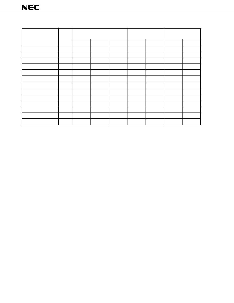
ELECTRICAL CHARACTERISTICS (T
A
= 25
±
2
∞
C)
Type Number
Class
Zener Voltage
Dynamic
Reverse Current
Vz (V)
Note 1
Impedance Zz (
)
Note 2
I
R
(
µ
A)
MIN.
MAX.
Iz (mA)
MAX.
Iz (mA)
MAX.
V
R
(V)
RD39S
B
37.00
41.00
2
100
2
2
30
RD43S
B
40.00
45.00
2
130
2
2
33
RD47S
B
44.00
49.00
2
150
2
2
36
RD51S
B
48.00
54.00
2
180
2
1
39
RD56S
B
53.00
60.00
2
180
2
1
43
RD62S
B
58.00
66.00
2
200
2
0.2
47
RD68S
B
64.00
72.00
2
250
2
0.2
52
RD75S
B
70.00
79.00
2
300
2
0.2
57
RD82S
B
77.00
87.00
2
300
2
0.2
63
RD91S
B
85.00
96.00
1
700
1
0.2
69
RD100S
B
94.00
106.0
1
700
1
0.2
76
RD110S
B
104.0
116.0
1
800
1
0.2
84
RD120S
B
114.0
126.0
1
900
1
0.2
91
Note 1. Vz is tested with pulsed (40 ms).
2. Zz is measured at Iz by given a very small A.C. current signal.
RD2.0S to RD120S
5
Data Sheet D11444EJ3V0DS00
TYPICAL CHARACTERISTICS (T
A
= 25
∞
C)
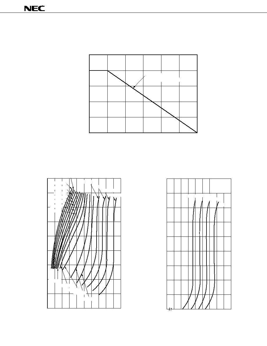
Fig. 1 POWER DISSIPATION vs. AMBIENT TEMPERATURE
Fig. 2 ZENER CURRENT vs. ZENER VOLTAGE
Fig. 3 ZENER CURRENT vs. ZENER VOLTAGE
250
200
150
100
50
0
0
25
50
75
100
125
150
T
A
- Ambient Temperature - ∞C
P - Power Dissipation - mW
30
◊
30
◊
1.6
P. C. B. (Glass Epoxy)
100 m
10 m
1 m
100
10
1
100 n
10 n
1 n
0
7
8
9
10 11
12 13
14 15
T
A
= 25 ∞C
TYP.
RD10S
RD12S
RD11S
RD13S
Vz - Zener Voltage - V
I
Z
- Zener Current - A
µ
µ
µ
100 m
10 m
1 m
100
10
1
100 n
10 n
1 n
0
10
1
2
3
4
5
6
7
8
9
V
Z
- Zener Voltage - V
I
Z
- Zener Current - A
RD3.9S
RD3.3S
RD2.4S
RD2.0S
RD2.2S
RD6.8S
RD9.1S
RD4.3S
RD4.7S
RD5.1S
RD6.2S
RD5.6S
RD7.5S
RD8.2S
RD3.0S
RD2.7S
RD3.6S
µ
µ
µ
RD2.0S to RD120S
6
Data Sheet D11444EJ3V0DS00
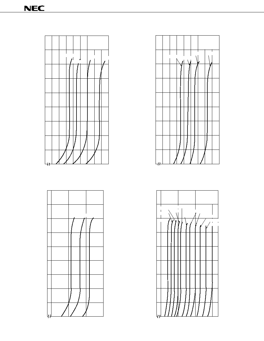
Fig. 4 ZENER CURRENT vs. ZENER VOLTAGE
Fig. 5 ZENER CURRENT vs. ZENER VOLTAGE
Fig. 6 ZENER CURRENT vs. ZENER VOLTAGE
Fig. 7 ZENER CURRENT vs. ZENER VOLTAGE
100 m
10 m
1 m
100
10
1
100 n
10 n
1 n
0
16
18
20
22 24
26 28
30 32
Iz - Zener Current - A
Vz - Zener Voltage - V
RD22S
RD27S
RD24S
RD30S
T
A
= 25 ∞C
TYP
µ
µ
µ
100 m
10 m
1 m
10
1
100 n
10 n
1 n
Vz - Zener Voltage - V
RD33S
Iz - Zener Current - A
100
0 25
30
35
40
RD36S
RD39S
T
A
= 25 ∞C
TYP
µ
µ
µ
100 m
10 m
1 m
10
1
100 n
10 n
1 n
RD56S
Iz - Zener Current - A
100
0 30
60
90
120
RD68S
Vz - Zener Voltage - V
RD47S
RD43S
RD62S
RD75S
RD82S
RD120S
RD110S
RD100S
RD91S
T
A
= 25 ∞C
TYP
µ
µ
µ
100 m
10 m
1 m
100
10
1
100 n
10 n
1 n
0
12
13
14
15 16
17 18
19 20
Iz - Zener Current - A
T
A
= 25 ∞C
TYP
Vz - Zener Voltage - V
RD15S
RD18S
RD16S
RD20S
µ
µ
µ
RD2.0S to RD120S
7
Data Sheet D11444EJ3V0DS00
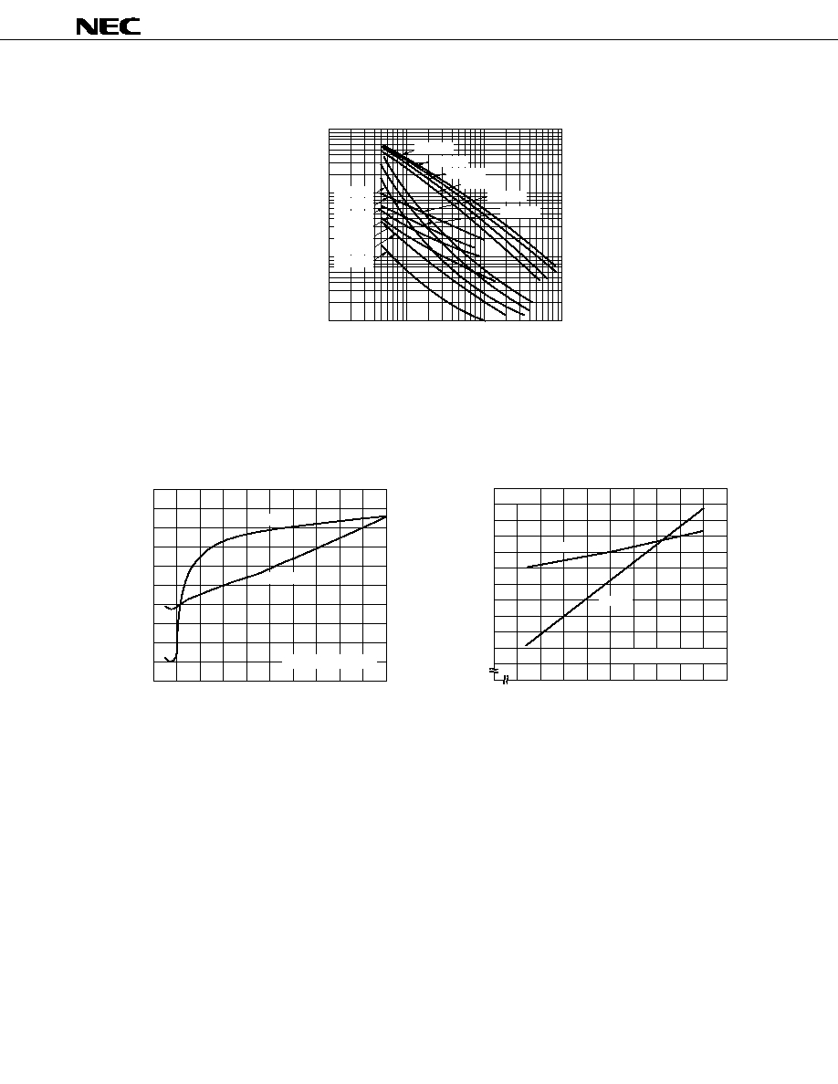
Fig. 8 DYNAMIC IMPEDANCE vs. ZENER CURRENT
Fig. 9
ZENER VOLTAGE TEMPERATURE
Fig. 10 ZENER VOLTAGE TEMPERATURE
COEFFICIENT vs. ZENER VOLTAGE
COEFFICIENT vs. ZENER VOLTAGE
0.12
0
20
60
80
100
120
140
Vz - Zener Voltage - V
TYP.
%/∞C
mV/∞C
RD43S to RD120S
0.11
0.10
0.09
0.08
0.07
40
50
60
70
80
90 100 110 120
40
Z
- Zener Voltage Temperature Coefficient - % / ∞C
Z
- Zener Voltage Temperature Coefficient - mV/ ∞C
0.1
1
10
100
1
10
100
1000
I
Z
- Zener Current - mA
Z
Z
- Zener Impedance -
RD5.6S
RD24S
RD20S
RD15S
RD10S
RD7.5S
RD2.0S
RD2.4S
RD3.0S
RD3.9S
RD4.7S
RD5.1S
RD39S
0.1
0.08
0.06
0.04
0.02
0
≠0.02
≠0.04
≠0.06
0
4
8
12
16
20
24
28
32
36
40
≠24
≠16
≠8
0
8
16
24
32
40
V
Z
- Zener Voltage - V
Z
- V
Z
Temperature Coefficient - mV/
∞
C
Z
- V
Z
Temperature Coefficient - %/
∞
C
%mV/
∞
C
%V/
∞
C
RD2.0S to RD39S
RD2.0S to RD120S
8
Data Sheet D11444EJ3V0DS00
Fig. 11 TRANSIENT THERMAL IMPEDANCE CHARACTERISTICS
Fig. 12 SURGE REVERSE POWER RATINGS
t - Time - s
Z
th
- Transient Thermal Impedance -∞C
1000
100
10
1m
10m
100m
1
10
100
5
5000
RD[ ]S
P.C.B (Glass Epoxy)
(30mm
◊
30mm
◊
1.6mm)
T
A
= 25 ∞C
Repetitive
P
RSM
t
T
1 000
100
10
1
1
10
100
1 m
10 m
100 m
t
T
- Pulse Width - s
P
RSM
- Surge Reverse Power - W
µ
µ
µ

RD2.0S to RD120S
9
Data Sheet D11444EJ3V0DS00
[MEMO]

RD2.0S to RD120S
10
Data Sheet D11444EJ3V0DS00
[MEMO]

RD2.0S to RD120S
11
Data Sheet D11444EJ3V0DS00
[MEMO]

RD2.0S to RD120S
[MEMO]
∑
The information in this document is subject to change without notice. Before using this document, please
confirm that this is the latest version.
∑
No part of this document may be copied or reproduced in any form or by any means without the prior written
consent of NEC Corporation. NEC Corporation assumes no responsibility for any errors which may appear in
this document.
∑
NEC Corporation does not assume any liability for infringement of patents, copyrights or other intellectual
property rights of third parties by or arising from use of a device described herein or any other liability arising
from use of such device. No license, either express, implied or otherwise, is granted under any patents, copyrights
or other intellectual property rights of NEC Corporation or others.
∑
Descriptions of circuits, software, and other related information in this document are provided for illustrative
purposes in semiconductor product operation and application examples. The incorporation of these circuits,
software, and information in the design of the customer's equipment shall be done under the full responsibility
of the customer. NEC Corporation assumes no responsibility for any losses incurred by the customer or third
parties arising from the use of these circuits, software, and information.
∑
While NEC Corporation has been making continuous effort to enhance the reliability of its semiconductor devices,
the possibility of defects cannot be eliminated entirely. To minimize risks of damage or injury to persons or
property arising from a defect in an NEC semiconductor device, customers must incorporate sufficient safety
measures in its design, such as redundancy, fire-containment, and anti-failure features.
∑
NEC devices are classified into the following three quality grades:
"Standard", "Special", and "Specific". The Specific quality grade applies only to devices developed based on a
customer designated "quality assurance program" for a specific application. The recommended applications of
a device depend on its quality grade, as indicated below. Customers must check the quality grade of each device
before using it in a particular application.
Standard: Computers, office equipment, communications equipment, test and measurement equipment,
audio and visual equipment, home electronic appliances, machine tools, personal electronic
equipment and industrial robots
Special:
Transportation equipment (automobiles, trains, ships, etc.), traffic control systems, anti-disaster
systems, anti-crime systems, safety equipment and medical equipment (not specifically designed
for life support)
Specific:
Aircraft, aerospace equipment, submersible repeaters, nuclear reactor control systems, life
support systems or medical equipment for life support, etc.
The quality grade of NEC devices is "Standard" unless otherwise specified in NEC's Data Sheets or Data Books.
If customers intend to use NEC devices for applications other than those specified for Standard quality grade,
they should contact an NEC sales representative in advance.
M7 98.8