 | –≠–ª–µ–∫—Ç—Ä–æ–Ω–Ω—ã–π –∫–æ–º–ø–æ–Ω–µ–Ω—Ç: UPA835TC | –°–∫–∞—á–∞—Ç—å:  PDF PDF  ZIP ZIP |
Caution Electro-static sensitive devices
The information in this document is subject to change without notice. Before using this document, please
confirm that this is the latest version.
Not all devices/types available in every country. Please check with local NEC representative for
availability and additional information.
NPN SILICON RF TWIN TRANSISTOR
µ
µ
µ
µ
PA835TC
NPN SILICON EPITAXIAL TRANSISTOR (WITH 2 DIFFERENT ELEMENTS)
IN A FLAT-LEAD 6-PIN THIN-TYPE ULTRA SUPER MINIMOLD PACKAGE
Document No. P14555EJ1V0DS00 (1st edition)
Date Published November 1999 N CP(K)
Printed in Japan
DATA SHEET
1999
©
DESCRIPTION
The
µ
PA835TC has built-in two different transistors (Q1 and Q2) for low noise amplification in the VHF band to
UHF band.
FEATURES
∑ Low noise
Q1 : NF = 1.5 dB TYP. @ f = 2 GHz, V
CE
= 3 V, I
C
= 3 mA
Q2 : NF = 1.2 dB TYP. @ f = 1 GHz, V
CE
= 3 V, I
C
= 7 mA
∑ High gain
Q1 :
|
S
21e
|
2
= 8.5 dB TYP. @ f = 2 GHz, V
CE
= 3 V, I
C
= 10 mA
Q2 :
|
S
21e
|
2
= 9.0 dB TYP. @ f = 1 GHz, V
CE
= 3 V, I
C
= 7 mA
∑ Flat-lead 6-pin thin-type ultra super minimold package
∑ Built-in 2 different transistors (2SC5010, 2SC5006)
BUILT-IN TRANSISTORS
Q1
Q2
3-pin ultra super minimold part No.
2SC5010
2SC5006
ORDERING INFORMATION
Part Number
Package
Quantity
Supplying Form
µ
PA835TC
Loose products
(50 pcs)
µ
PA835TC-T1
Flat-lead 6-pin
thin-type ultra
super minimold
Taping products
(3 kp/reel)
8 mm wide embossed tape.
Pin 6 (Q1 Base), pin 5 (Q2 Emitter), pin 4 (Q2 Base) face to perforation
side of the tape.
Remark To order evaluation samples, please contact your local NEC sales office. (Part number for sample order:
µ
PA835TC.)

Data Sheet P14555EJ1V0DS00
2
µ
µ
µ
µ
PA835TC
ABSOLUTE MAXIMUM RATINGS (T
A
= +25
∞
∞
∞
∞
C)
Ratings
Parameter
Symbol
Q1
Q2
Unit
Collector to Base Voltage
V
CBO
9
20
V
Collector to Emitter Voltage
V
CEO
6
12
V
Emitter to Base Voltage
V
EBO
2
3
V
Collector Current
I
C
30
100
mA
Total Power Dissipation
P
T
Note
180 in 1 element
200 in 1 element
mW
230 in 2 elements
Junction Temperature
T
j
150
150
∞
C
Storage Temperature
T
stg
-
65 to +150
∞
C
Note Mounted on 1.08 cm
2
◊
1.0 mm glass epoxy substrate.
ELECTRICAL CHARACTERISTICS (T
A
= +25
∞
∞
∞
∞
C)
(1) Q1
Parameter
Symbol
Conditions
MIN.
TYP.
MAX.
Unit
Collector Cutoff Current
I
CBO
V
CB
= 5 V, I
E
= 0
-
-
0.1
µ
A
Emitter Cutoff Current
I
EBO
V
EB
= 1 V, I
C
= 0
-
-
0.1
µ
A
DC Current Gain
h
FE
V
CE
= 3 V, I
C
= 10 mA
Note 1
75
-
150
Gain Bandwidth Product
f
T
V
CE
= 3 V, I
C
= 10 mA, f = 2 GHz
10.0
12.0
-
GHz
Feedback Capacitance
C
re
V
CB
= 3 V, I
E
= 0, f = 1 MHz
Note 2
-
0.4
0.7
pF
Insertion Power Gain
|
S
21e
|
2
V
CE
= 3 V, I
C
= 10 mA, f = 2 GHz
7.0
8.5
-
dB
Noise Figure
NF
V
CE
= 3 V, I
C
= 3 mA, f = 2 GHz
-
1.5
2.5
dB
Notes 1. Pulse Measurement: PW
350
µ
s, Duty Cycle
2%
2. Collector to base capacitance when measured with capacitance meter (automatic balanced bridge
method), with emitter connected to guard pin of capacitance meter.
Data Sheet P14555EJ1V0DS00
3
µ
µ
µ
µ
PA835TC
(2) Q2
Parameter
Symbol
Conditions
MIN.
TYP.
MAX.
Unit
Collector Cutoff Current
I
CBO
V
CB
= 10 V, I
E
= 0
-
-
1.0
µ
A
Emitter Cutoff Current
I
EBO
V
EB
= 1 V, I
C
= 0
-
-
1.0
µ
A
DC Current Gain
h
FE
V
CE
= 3 V, I
C
= 7 mA
Note 1
70
-
140
Gain Bandwidth Product
f
T
V
CE
= 3 V, I
C
= 7 mA, f = 1 GHz
3.0
4.5
-
GHz
Feedback Capacitance
C
re
V
CB
= 3 V, I
E
= 0, f = 1 MHz
Note 2
-
0.7
1.5
pF
Insertion Power Gain
|
S
21e
|
2
V
CE
= 3 V, I
C
= 7 mA, f = 1 GHz
7.0
9.0
-
dB
Noise Figure
NF
V
CE
= 3 V, I
C
= 7 mA, f = 1 GHz
-
1.2
2.5
dB
Notes 1. Pulse Measurement: PW
350
µ
s, Duty Cycle
2%
2. Collector to base capacitance when measured with capacitance meter (automatic balanced bridge
method), with emitter connected to guard pin of capacitance meter.
h
FE
CLASSIFICATION
Rank
FB
Marking
37
h
FE
Value of Q1
75 to 150
h
FE
Value of Q2
70 to 140
Data Sheet P14555EJ1V0DS00
4
µ
µ
µ
µ
PA835TC
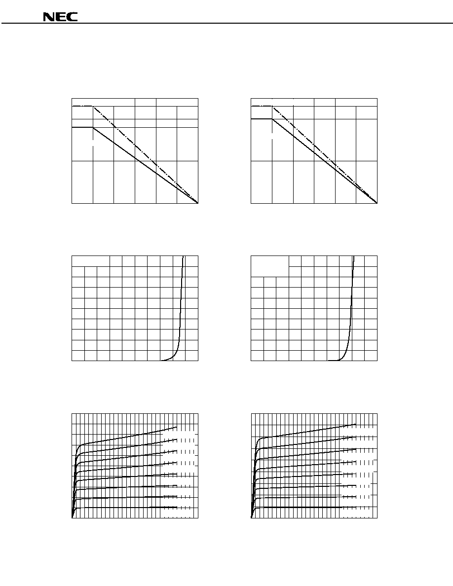
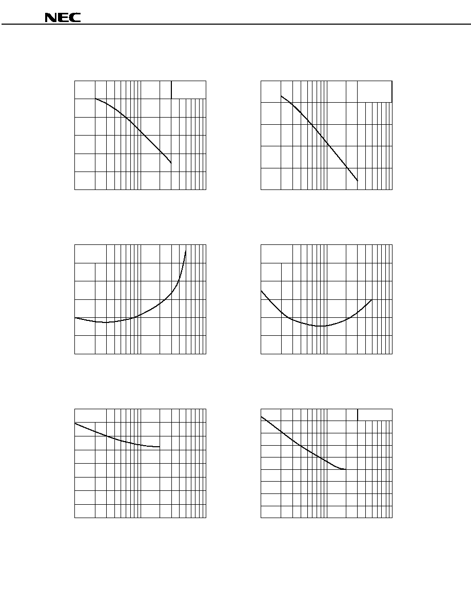
TYPICAL CHARACTERISTICS (T
A
= +25
∞
∞
∞
∞
C)
Total Power Dissipation P
T
(mW)
Ambient Temperature T
A
(
∞
C)
Total Power Dissipation P
T
(mW)
Ambient Temperature T
A
(
∞
C)
TOTAL POWER DISSIPATION vs.
AMBIENT TEMPERATURE
Collector Current I
C
(mA)
Collector to Emitter Voltage V
CE
(V)
COLLECTOR CURRENT vs.
COLLECTOR TO EMITTER VOLTAGE
Collector Current I
C
(mA)
Base to Emitter Voltage V
BE
(V)
COLLECTOR CURRENT vs.
BASE TO EMITTER VOLTAGE
Collector Current I
C
(mA)
Collector to Emitter Voltage V
CE
(V)
COLLECTOR CURRENT vs.
COLLECTOR TO EMITTER VOLTAGE
Collector Current I
C
(mA)
Base to Emitter Voltage V
BE
(V)
COLLECTOR CURRENT vs.
BASE TO EMITTER VOLTAGE
TOTAL POWER DISSIPATION vs.
AMBIENT TEMPERATURE
0
0
50
100
150
100
180
200
230
2 Elements in total
Free Air
Free Air
Per
Element (Q1)
0
0
50
100
150
100
200
230
2 Elements in total
Per
Element (Q2)
10
20
30
40
50
0.5
1.0
V
CE
= 3 V
10
20
0.5
1.0
V
CE
= 3 V
I
B
= 160 A
µ
I
B
= 140 A
µ
I
B
= 120 A
µ
I
B
= 100 A
µ
I
B
= 80 A
µ
I
B
= 60 A
µ
I
B
= 40 A
µ
I
B
= 20 A
µ
0
0
2
4
6
8
10
12
14
16
18
20
1
2
3
4
5
6
0
0
0
0
I
B
= 160 A
µ
I
B
= 140 A
µ
I
B
= 120 A
µ
I
B
= 100 A
µ
I
B
= 80 A
µ
I
B
= 60 A
µ
I
B
= 40 A
µ
I
B
= 20 A
µ
0
0
2
4
6
8
10
12
14
16
18
1
2
3
4
5
6
Q1
Q2
Data Sheet P14555EJ1V0DS00
5
µ
µ
µ
µ
PA835TC
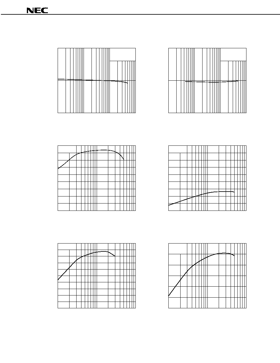
DC Current Gain h
FE
Collector Current I
C
(mA)
DC Current Gain h
FE
Collector Current I
C
(mA)
DC CURRENT GAIN vs.
COLLECTOR CURRENT
Insertion Power Gain
S
21e
2
(dB)
Collector Current I
C
(mA)
INSERTION POWER GAIN vs.
COLLECTOR CURRENT
Gain Bandwidth Product f
T
(GHz)
Collector Current I
C
(mA)
GAIN BANDWIDTH PRODUCT vs.
COLLECTOR CURRENT
Insertion Power Gain
S
21e
2
(dB)
Collector Current I
C
(mA)
INSERTION POWER GAIN vs.
COLLECTOR CURRENT
Gain Bandwidth Product f
T
(GHz)
Collector Current I
C
(mA)
GAIN BANDWIDTH PRODUCT vs.
COLLECTOR CURRENT
DC CURRENT GAIN vs.
COLLECTOR CURRENT
10
0.1
100
1 000
1
10
100
V
CE
= 3 V
10
0.1
100
1 000
1
10
100
V
CE
= 3 V
0.00
1
2.00
4.00
6.00
8.00
10.00
12.00
14.00
16.00
18.00
10
100
V
CE
= 3 V
f = 2 GHz
0.00
1
2.00
4.00
6.00
8.00
10.00
12.00
14.00
16.00
18.00
10
100
V
CE
= 3 V
f = 1 GHz
2.00
3.00
4.00
5.00
6.00
7.00
8.00
9.00
10.00
11.00
12.00
1
10
100
V
CE
= 3 V
f = 2 GHz
2.00
4.00
6.00
8.00
10.00
12.00
14.00
1
10
100
V
CE
= 3 V
f = 1 GHz
Q1
Q2
Data Sheet P14555EJ1V0DS00
6
µ
µ
µ
µ
PA835TC
Insertion Power Gain
S
21e
2
(dB)
Frequency f (GHz)
Insertion Power Gain
S
21e
2
(dB)
Frequency f (GHz)
INSERTION POWER GAIN vs. FREQUENCY
Feedback Capacitance C
re
(pF)
Collector to Base Voltage V
CB
(V)
FEEDBACK CAPACITANCE vs.
COLLECTOR TO BASE VOLTAGE
Noise Figure NF (dB)
Collector Current I
C
(mA)
NOISE FIGURE vs. COLLECTOR CURRENT
Feedback Capacitance C
re
(pF)
Collector to Base Voltage V
CB
(V)
FEEDBACK CAPACITANCE vs.
COLLECTOR TO BASE VOLTAGE
Noise Figure NF (dB)
Collector Current I
C
(mA)
NOISE FIGURE vs. COLLECTOR CURRENT
INSERTION POWER GAIN vs. FREQUENCY
Q1
Q2
0.0
0.1
5.0
10.0
15.0
20.0
25.0
30.0
1.0
10.0
V
CE
= 3 V
I
C
= 10 mA
0.0
0.1
5.0
10.0
15.0
20.0
25.0
1.0
10.0
V
CE
= 3 V
I
C
= 7 mA
0.00
1.00
2.00
3.00
4.00
5.00
6.00
1
10
100
V
CE
= 3 V
f = 2 GHz
0.00
1.00
2.00
3.00
4.00
5.00
6.00
1
10
100
V
CE
= 3 V
f = 1 GHz
0.000
0.050
0.100
0.150
0.200
0.350
0.400
1
10
100
0.250
0.300
f = 1 MHz
0.000
0.100
0.200
0.300
0.400
0.700
0.900
1
10
100
0.500
0.600
0.800
f = 1 MHz

Data Sheet P14555EJ1V0DS00
7
µ
µ
µ
µ
PA835TC
S-PARAMETERS Q1
V
CE
= 3 V, I
C
= 1 mA
FREQUENCY
S
11
S
21
S
12
S
22
GHz
MAG.
ANG.
MAG.
ANG.
MAG.
ANG.
MAG.
ANG.
0.1
0.946
-
13.6
3.770
166.9
0.023
55.8
0.993
-
9.9
0.2
0.943
-
25.7
3.643
154.2
0.044
73.9
0.987
-
18.7
0.3
0.934
-
37.8
3.536
143.0
0.060
52.7
0.984
-
28.4
0.4
0.906
-
50.2
3.450
130.5
0.072
51.6
0.966
-
37.4
0.5
0.887
-
62.5
3.393
118.9
0.086
41.2
0.943
-
46.6
0.6
0.846
-
74.8
3.268
107.2
0.104
31.0
0.923
-
55.6
0.7
0.818
-
87.0
3.188
95.8
0.113
21.0
0.896
-
63.8
0.8
0.773
-
98.7
3.077
84.5
0.126
11.0
0.866
-
72.6
0.9
0.738
-
110.6
2.980
73.4
0.137
4.3
0.845
-
81.0
1.0
0.704
-
122.4
2.887
62.8
0.148
-
4.7
0.820
-
89.4
1.1
0.665
-
134.1
2.796
52.2
0.153
-
14.1
0.787
-
97.8
1.2
0.630
-
146.0
2.715
42.0
0.163
-
21.6
0.767
-
105.3
1.3
0.597
-
158.1
2.619
31.5
0.170
-
29.8
0.741
-
113.4
1.4
0.566
-
170.1
2.540
21.7
0.175
-
36.9
0.713
-
121.3
1.5
0.536
178.4
2.455
11.9
0.181
-
45.4
0.690
-
129.0
1.6
0.507
165.6
2.381
1.8
0.186
-
53.0
0.668
-
136.5
1.7
0.480
153.4
2.302
-
8.0
0.190
-
60.0
0.647
-
144.4
1.8
0.456
141.3
2.236
-
17.5
0.192
-
67.5
0.627
-
152.0
1.9
0.436
129.0
2.175
-
26.7
0.195
-
75.2
0.603
-
159.1
2.0
0.423
116.0
2.109
-
36.2
0.196
-
81.3
0.590
-
166.5
2.1
0.405
102.6
2.039
-
45.6
0.200
-
88.8
0.567
-
173.9
2.2
0.391
90.6
1.977
-
54.9
0.202
-
95.4
0.551
178.2
2.3
0.381
78.0
1.916
-
63.8
0.202
-
101.9
0.536
171.0
2.4
0.376
65.1
1.863
-
72.8
0.205
-
108.2
0.519
163.2
2.5
0.369
52.6
1.808
-
81.7
0.207
-
115.2
0.504
155.7
2.6
0.371
40.4
1.757
-
90.6
0.207
-
121.8
0.490
147.7
2.7
0.368
28.5
1.701
-
99.1
0.211
-
127.1
0.475
140.0
2.8
0.371
17.0
1.652
-
107.6
0.207
-
133.5
0.463
132.3
2.9
0.376
5.5
1.611
-
115.9
0.208
-
139.3
0.451
124.7
3.0
0.380
-
5.4
1.564
-
124.4
0.211
-
145.1
0.442
116.8
V
CE
= 3 V, I
C
= 3 mA
FREQUENCY
S
11
S
21
S
12
S
22
GHz
MAG.
ANG.
MAG.
ANG.
MAG.
ANG.
MAG.
ANG.
0.1
0.886
-
19.0
9.528
161.8
0.010
47.7
0.978
-
13.2
0.2
0.851
-
34.6
8.889
146.3
0.043
67.8
0.961
-
24.9
0.3
0.804
-
51.0
8.377
131.9
0.050
52.1
0.919
-
37.0
0.4
0.745
-
66.6
7.805
117.1
0.063
41.6
0.867
-
47.7
0.5
0.691
-
81.2
7.343
103.9
0.075
38.4
0.809
-
57.5
0.6
0.623
-
95.0
6.732
91.0
0.088
28.1
0.757
-
66.8
0.7
0.571
-
109.2
6.288
79.0
0.089
15.7
0.707
-
75.5
0.8
0.522
-
122.1
5.843
67.6
0.099
9.7
0.664
-
84.0
0.9
0.473
-
135.3
5.404
56.9
0.107
2.2
0.628
-
91.8
1.0
0.433
-
148.0
5.052
46.5
0.111
-
4.5
0.589
-
99.4
1.1
0.394
-
160.7
4.730
36.6
0.119
-
13.2
0.562
-
106.7
1.2
0.361
-
173.5
4.453
26.8
0.125
-
18.2
0.534
-
114.0
1.3
0.338
173.5
4.187
17.4
0.130
-
25.5
0.507
-
121.5
1.4
0.312
160.3
3.966
8.1
0.134
-
30.9
0.486
-
128.4
1.5
0.295
147.5
3.764
-
0.9
0.137
-
37.2
0.464
-
135.6
1.6
0.281
133.8
3.571
-
9.9
0.144
-
43.6
0.445
-
142.7
1.7
0.271
120.5
3.395
-
18.5
0.151
-
50.0
0.427
-
150.0
1.8
0.263
106.6
3.230
-
27.4
0.155
-
56.1
0.412
-
156.9
1.9
0.257
93.7
3.109
-
35.9
0.160
-
62.3
0.397
-
164.6
2.0
0.255
80.0
2.974
-
44.7
0.165
-
68.1
0.382
-
171.3
2.1
0.257
67.0
2.860
-
52.8
0.170
-
74.6
0.368
-
178.4
2.2
0.265
54.9
2.747
-
61.6
0.177
-
81.5
0.351
173.2
2.3
0.271
41.9
2.644
-
69.6
0.180
-
87.8
0.335
165.5
2.4
0.279
29.9
2.541
-
78.1
0.184
-
93.9
0.319
157.9
2.5
0.284
18.1
2.444
-
86.1
0.192
-
100.3
0.305
150.4
2.6
0.296
7.8
2.367
-
94.4
0.196
-
106.2
0.294
141.8
2.7
0.304
-
2.6
2.287
-
102.2
0.200
-
111.9
0.281
133.6
2.8
0.315
-
12.1
2.209
-
110.2
0.205
-
118.9
0.273
125.9
2.9
0.328
-
21.9
2.144
-
118.1
0.209
-
124.8
0.261
117.8
3.0
0.341
-
31.2
2.062
-
125.9
0.213
-
130.8
0.248
108.6

Data Sheet P14555EJ1V0DS00
8
µ
µ
µ
µ
PA835TC
V
CE
= 3 V, I
C
= 5 mA
FREQUENCY
S
11
S
21
S
12
S
22
GHz
MAG.
ANG.
MAG.
ANG.
MAG.
ANG.
MAG.
ANG.
0.1
0.826
-
23.1
13.981
158.4
0.015
70.3
0.961
-
15.5
0.2
0.764
-
40.7
12.736
140.4
0.038
65.2
0.921
-
29.3
0.3
0.699
-
59.2
11.601
124.1
0.045
54.5
0.846
-
42.2
0.4
0.619
-
76.9
10.428
108.4
0.056
43.7
0.773
-
53.1
0.5
0.546
-
92.0
9.448
94.8
0.061
35.3
0.701
-
63.1
0.6
0.481
-
106.8
8.471
81.9
0.071
25.2
0.642
-
71.5
0.7
0.427
-
120.9
7.641
70.2
0.076
14.9
0.598
-
79.4
0.8
0.378
-
134.3
6.949
59.6
0.084
8.9
0.555
-
86.6
0.9
0.336
-
147.3
6.379
49.3
0.091
4.7
0.521
-
93.8
1.0
0.303
-
160.6
5.868
39.3
0.098
-
0.5
0.488
-
100.9
1.1
0.276
-
174.5
5.433
29.8
0.104
-
8.0
0.465
-
107.9
1.2
0.250
172.2
5.069
20.8
0.111
-
13.4
0.437
-
114.2
1.3
0.237
158.8
4.735
11.7
0.115
-
18.9
0.420
-
121.2
1.4
0.217
144.3
4.448
3.1
0.118
-
26.5
0.403
-
127.6
1.5
0.212
130.2
4.185
-
5.5
0.127
-
31.8
0.385
-
134.9
1.6
0.206
115.4
3.952
-
14.2
0.135
-
37.9
0.369
-
141.9
1.7
0.204
101.8
3.751
-
22.7
0.140
-
42.7
0.356
-
149.4
1.8
0.202
88.1
3.580
-
31.0
0.147
-
49.5
0.341
-
155.9
1.9
0.206
74.8
3.417
-
39.1
0.154
-
56.0
0.328
-
163.7
2.0
0.212
61.5
3.249
-
47.4
0.160
-
61.7
0.314
-
170.1
2.1
0.220
49.0
3.122
-
55.6
0.164
-
68.7
0.300
-
177.9
2.2
0.227
37.6
2.981
-
63.9
0.171
-
74.9
0.288
174.4
2.3
0.235
26.5
2.875
-
71.7
0.177
-
81.0
0.276
166.6
2.4
0.246
15.7
2.761
-
79.7
0.181
-
87.6
0.261
159.1
2.5
0.258
5.8
2.657
-
87.5
0.189
-
94.3
0.249
150.7
2.6
0.272
-
4.3
2.564
-
95.4
0.198
-
99.4
0.240
142.6
2.7
0.282
-
13.0
2.475
-
103.1
0.203
-
106.3
0.229
134.4
2.8
0.295
-
21.6
2.391
-
111.0
0.208
-
113.5
0.217
125.9
2.9
0.308
-
30.8
2.325
-
118.6
0.214
-
119.7
0.209
117.3
3.0
0.319
-
38.9
2.244
-
126.5
0.220
-
125.5
0.201
107.5
V
CE
= 3 V, I
C
= 10 mA
FREQUENCY
S
11
S
21
S
12
S
22
GHz
MAG.
ANG.
MAG.
ANG.
MAG.
ANG.
MAG.
ANG.
0.1
0.712
-
27.5
20.853
152.8
0.023
40.4
0.950
-
19.6
0.2
0.619
-
52.5
18.111
131.2
0.028
57.0
0.836
-
35.5
0.3
0.527
-
71.9
15.435
113.2
0.042
46.6
0.746
-
48.6
0.4
0.436
-
90.0
13.155
97.4
0.049
44.8
0.644
-
57.8
0.5
0.371
-
105.6
11.390
84.1
0.056
37.1
0.577
-
66.2
0.6
0.312
-
120.8
9.922
72.0
0.059
30.3
0.523
-
73.5
0.7
0.267
-
135.3
8.761
61.5
0.066
22.2
0.479
-
80.0
0.8
0.235
-
150.0
7.816
51.3
0.076
17.4
0.446
-
85.8
0.9
0.207
-
163.7
7.036
42.0
0.083
10.7
0.421
-
92.9
1.0
0.181
-
178.6
6.440
32.6
0.089
6.5
0.398
-
98.7
1.1
0.167
165.4
5.906
23.6
0.098
0.1
0.379
-
105.5
1.2
0.155
150.2
5.465
15.2
0.102
-
5.5
0.361
-
111.2
1.3
0.151
134.6
5.071
6.8
0.109
-
13.0
0.350
-
118.4
1.4
0.148
120.2
4.753
-
1.5
0.117
-
17.5
0.335
-
124.6
1.5
0.147
105.1
4.471
-
9.9
0.125
-
23.3
0.326
-
131.9
1.6
0.153
90.9
4.202
-
18.0
0.134
-
30.1
0.310
-
138.8
1.7
0.159
77.9
3.989
-
26.1
0.140
-
37.7
0.298
-
145.5
1.8
0.169
65.0
3.779
-
34.1
0.148
-
43.3
0.289
-
152.9
1.9
0.176
52.7
3.612
-
41.9
0.156
-
49.7
0.275
-
160.9
2.0
0.187
41.9
3.430
-
50.0
0.162
-
56.2
0.265
-
167.8
2.1
0.202
31.7
3.291
-
57.6
0.168
-
63.0
0.253
-
174.8
2.2
0.212
21.2
3.144
-
65.8
0.177
-
69.5
0.241
176.8
2.3
0.227
11.6
3.026
-
73.3
0.183
-
75.7
0.228
168.8
2.4
0.235
2.4
2.908
-
81.2
0.188
-
83.0
0.217
160.8
2.5
0.249
-
6.3
2.799
-
88.8
0.197
-
89.9
0.203
151.7
2.6
0.268
-
14.7
2.703
-
96.9
0.203
-
96.1
0.195
142.5
2.7
0.278
-
23.3
2.608
-
104.3
0.208
-
102.3
0.184
133.7
2.8
0.291
-
31.1
2.514
-
111.9
0.216
-
109.6
0.176
124.8
2.9
0.302
-
39.7
2.444
-
119.6
0.222
-
116.1
0.165
115.4
3.0
0.317
-
47.1
2.352
-
127.0
0.228
-
122.8
0.157
105.1

Data Sheet P14555EJ1V0DS00
9
µ
µ
µ
µ
PA835TC
S-PARAMETERS Q2
V
CE
= 3 V, I
C
= 1 mA
FREQUENCY
S
11
S
21
S
12
S
22
GHz
MAG.
ANG.
MAG.
ANG.
MAG.
ANG.
MAG.
ANG.
0.1
0.941
-
30.0
3.791
157.1
0.037
54.8
0.985
-
13.1
0.2
0.910
-
57.7
3.421
137.0
0.085
54.6
0.946
-
25.6
0.3
0.883
-
82.7
3.092
119.2
0.107
36.1
0.897
-
37.2
0.4
0.848
-
106.0
2.773
101.9
0.125
21.4
0.840
-
47.4
0.5
0.819
-
125.9
2.502
86.6
0.136
9.1
0.792
-
56.4
0.6
0.783
-
144.6
2.233
72.6
0.144
-
2.4
0.757
-
64.6
0.7
0.771
-
161.7
2.034
59.3
0.147
-
13.3
0.721
-
73.0
0.8
0.760
-
176.9
1.862
46.9
0.151
-
22.8
0.692
-
80.8
0.9
0.749
168.9
1.704
35.4
0.150
-
30.1
0.674
-
88.8
1.0
0.744
155.5
1.575
24.1
0.148
-
38.4
0.659
-
96.6
1.1
0.741
143.0
1.465
13.5
0.144
-
47.4
0.644
-
104.4
1.2
0.740
130.7
1.371
2.9
0.140
-
54.4
0.630
-
112.9
1.3
0.739
119.3
1.288
-
6.9
0.138
-
59.6
0.622
-
121.1
1.4
0.742
108.4
1.220
-
16.9
0.132
-
66.2
0.613
-
129.2
1.5
0.746
97.7
1.152
-
26.7
0.125
-
71.7
0.604
-
138.1
1.6
0.744
87.3
1.090
-
36.1
0.124
-
76.2
0.594
-
146.4
1.7
0.749
77.5
1.042
-
45.2
0.118
-
78.7
0.590
-
155.6
1.8
0.750
67.5
0.992
-
54.6
0.113
-
81.9
0.585
-
164.7
1.9
0.755
58.0
0.952
-
63.4
0.112
-
84.9
0.579
-
173.9
2.0
0.756
48.9
0.905
-
72.3
0.111
-
86.3
0.571
177.0
2.1
0.759
39.5
0.872
-
81.0
0.109
-
89.1
0.566
167.4
2.2
0.759
30.6
0.835
-
89.6
0.108
-
89.9
0.563
157.8
2.3
0.770
21.8
0.804
-
97.8
0.113
-
89.4
0.557
147.6
2.4
0.769
13.0
0.772
-
106.1
0.117
-
91.1
0.554
137.3
2.5
0.772
4.5
0.742
-
113.8
0.122
-
93.8
0.553
126.9
2.6
0.774
-
3.5
0.715
-
121.7
0.134
-
95.2
0.552
116.5
2.7
0.780
-
12.1
0.689
-
129.2
0.145
-
98.5
0.550
105.9
2.8
0.783
-
19.9
0.666
-
136.6
0.156
-
103.0
0.551
95.2
2.9
0.784
-
28.2
0.645
-
143.8
0.168
-
107.0
0.546
84.2
3.0
0.789
-
35.9
0.623
-
151.2
0.182
-
111.9
0.552
73.1
V
CE
= 3 V, I
C
= 3 mA
FREQUENCY
S
11
S
21
S
12
S
22
GHz
MAG.
ANG.
MAG.
ANG.
MAG.
ANG.
MAG.
ANG.
0.1
0.836
-
42.5
9.801
149.7
0.043
42.3
0.953
-
21.0
0.2
0.790
-
78.7
8.213
126.2
0.064
40.9
0.826
-
38.5
0.3
0.738
-
107.1
6.904
107.1
0.083
31.7
0.718
-
51.3
0.4
0.694
-
132.1
5.769
90.2
0.090
16.5
0.627
-
61.4
0.5
0.663
-
152.4
4.943
76.2
0.096
9.0
0.553
-
68.9
0.6
0.654
-
168.9
4.289
63.3
0.100
2.8
0.504
-
76.5
0.7
0.639
175.3
3.768
51.8
0.101
-
7.8
0.468
-
83.7
0.8
0.636
162.0
3.367
41.3
0.105
-
13.9
0.442
-
90.7
0.9
0.633
149.6
3.041
30.9
0.109
-
18.9
0.422
-
97.3
1.0
0.630
137.6
2.776
20.9
0.109
-
22.6
0.400
-
104.6
1.1
0.632
126.7
2.549
11.2
0.111
-
29.0
0.386
-
112.1
1.2
0.630
115.7
2.365
1.7
0.114
-
33.2
0.370
-
119.3
1.3
0.637
105.7
2.205
-
7.5
0.116
-
38.0
0.359
-
127.1
1.4
0.640
95.4
2.061
-
16.6
0.120
-
42.3
0.351
-
134.4
1.5
0.644
86.5
1.945
-
25.4
0.119
-
46.3
0.339
-
143.3
1.6
0.650
77.0
1.832
-
34.7
0.124
-
50.6
0.328
-
151.1
1.7
0.657
68.0
1.739
-
43.3
0.128
-
54.2
0.322
-
160.4
1.8
0.659
59.1
1.656
-
52.1
0.130
-
58.9
0.315
-
168.5
1.9
0.665
50.3
1.581
-
60.4
0.137
-
63.8
0.310
-
178.2
2.0
0.667
41.7
1.504
-
69.2
0.142
-
67.6
0.300
173.0
2.1
0.674
33.0
1.441
-
77.5
0.148
-
73.0
0.291
164.2
2.2
0.675
25.0
1.378
-
86.1
0.155
-
77.1
0.288
154.1
2.3
0.687
16.5
1.329
-
94.0
0.159
-
81.3
0.283
142.9
2.4
0.690
8.5
1.277
-
102.3
0.168
-
86.6
0.278
132.8
2.5
0.694
0.6
1.228
-
110.1
0.176
-
91.5
0.273
121.6
2.6
0.699
-
7.7
1.180
-
118.5
0.184
-
97.0
0.273
111.0
2.7
0.707
-
14.9
1.145
-
125.9
0.195
-
102.6
0.272
99.8
2.8
0.708
-
22.8
1.103
-
133.9
0.202
-
108.5
0.273
88.1
2.9
0.716
-
30.5
1.069
-
141.8
0.209
-
113.6
0.274
76.8
3.0
0.722
-
37.9
1.032
-
149.6
0.221
-
119.6
0.282
65.9

Data Sheet P14555EJ1V0DS00
10
µ
µ
µ
µ
PA835TC
V
CE
= 3 V, I
C
= 5 mA
FREQUENCY
S
11
S
21
S
12
S
22
GHz
MAG.
ANG.
MAG.
ANG.
MAG.
ANG.
MAG.
ANG.
0.1
0.780
-
51.3
13.572
145.3
0.043
33.0
0.919
-
28.3
0.2
0.716
-
90.8
10.762
120.1
0.062
39.6
0.745
-
44.8
0.3
0.665
-
120.8
8.650
100.9
0.068
30.1
0.617
-
58.5
0.4
0.625
-
144.3
7.032
85.1
0.077
20.8
0.523
-
67.8
0.5
0.611
-
164.1
5.914
71.6
0.081
13.3
0.456
-
75.6
0.6
0.598
-
179.7
5.042
59.6
0.086
7.2
0.405
-
82.1
0.7
0.592
166.4
4.436
49.0
0.091
-
0.3
0.371
-
89.1
0.8
0.592
153.6
3.929
38.6
0.092
-
6.5
0.342
-
95.1
0.9
0.593
141.8
3.527
28.9
0.100
-
9.0
0.323
-
101.9
1.0
0.594
130.9
3.208
19.3
0.101
-
14.1
0.304
-
108.2
1.1
0.601
120.6
2.948
10.0
0.107
-
18.5
0.291
-
116.1
1.2
0.598
110.4
2.723
0.9
0.112
-
24.0
0.278
-
123.6
1.3
0.602
100.8
2.535
-
7.9
0.116
-
28.3
0.266
-
130.6
1.4
0.604
91.6
2.372
-
16.7
0.120
-
33.9
0.256
-
138.4
1.5
0.618
82.4
2.222
-
25.6
0.127
-
38.6
0.247
-
147.0
1.6
0.615
73.2
2.095
-
34.2
0.132
-
43.5
0.235
-
155.5
1.7
0.625
64.7
1.986
-
43.0
0.138
-
47.9
0.229
-
164.3
1.8
0.628
56.0
1.884
-
51.5
0.144
-
52.6
0.222
-
172.9
1.9
0.636
47.5
1.802
-
59.8
0.151
-
58.1
0.213
177.9
2.0
0.638
39.2
1.712
-
68.2
0.156
-
63.3
0.208
168.5
2.1
0.647
30.9
1.636
-
76.4
0.165
-
69.3
0.198
158.0
2.2
0.649
22.7
1.568
-
84.9
0.172
-
74.2
0.196
147.6
2.3
0.661
14.8
1.509
-
92.8
0.177
-
79.1
0.188
135.8
2.4
0.663
6.7
1.450
-
100.9
0.186
-
85.4
0.186
124.6
2.5
0.665
-
0.9
1.397
-
108.7
0.194
-
91.5
0.184
112.4
2.6
0.677
-
8.9
1.346
-
116.9
0.202
-
97.9
0.185
101.4
2.7
0.686
-
16.1
1.307
-
124.5
0.211
-
103.2
0.186
88.4
2.8
0.684
-
23.9
1.255
-
132.3
0.218
-
110.2
0.187
76.4
2.9
0.693
-
31.4
1.218
-
140.0
0.226
-
115.1
0.188
64.5
3.0
0.700
-
38.7
1.171
-
147.8
0.237
-
121.4
0.197
53.0
V
CE
= 3 V, I
C
= 7 mA
FREQUENCY
S
11
S
21
S
12
S
22
GHz
MAG.
ANG.
MAG.
ANG.
MAG.
ANG.
MAG.
ANG.
0.1
0.799
-
44.6
13.333
147.7
0.052
43.2
0.934
-
26.4
0.2
0.712
-
83.9
10.995
123.0
0.068
47.2
0.769
-
46.0
0.3
0.653
-
112.1
8.986
103.9
0.081
32.7
0.642
-
61.2
0.4
0.614
-
136.6
7.380
87.8
0.084
21.4
0.533
-
72.0
0.5
0.593
-
156.5
6.275
74.0
0.090
17.0
0.456
-
80.3
0.6
0.577
-
172.8
5.389
62.1
0.096
9.8
0.399
-
88.8
0.7
0.567
171.9
4.692
50.9
0.104
0.2
0.361
-
96.3
0.8
0.565
158.8
4.188
40.6
0.110
-
5.6
0.322
-
102.6
0.9
0.560
146.9
3.768
30.7
0.113
-
8.9
0.298
-
109.6
1.0
0.557
135.3
3.427
21.1
0.117
-
15.0
0.276
-
116.8
1.1
0.563
124.5
3.149
11.6
0.123
-
20.4
0.260
-
124.7
1.2
0.564
113.9
2.907
2.5
0.126
-
24.7
0.242
-
131.6
1.3
0.569
104.4
2.713
-
6.4
0.130
-
30.1
0.225
-
139.1
1.4
0.570
94.3
2.525
-
15.3
0.139
-
35.6
0.214
-
147.4
1.5
0.579
85.4
2.379
-
24.2
0.146
-
40.1
0.204
-
156.1
1.6
0.582
76.0
2.249
-
32.8
0.151
-
46.8
0.193
-
164.2
1.7
0.586
67.6
2.130
-
41.2
0.159
-
50.9
0.183
-
173.7
1.8
0.586
58.7
2.014
-
49.7
0.164
-
56.7
0.175
178.3
1.9
0.595
50.4
1.928
-
57.9
0.173
-
63.0
0.166
167.4
2.0
0.600
41.6
1.836
-
66.7
0.178
-
68.1
0.160
157.5
2.1
0.611
33.5
1.758
-
74.8
0.183
-
74.2
0.148
147.0
2.2
0.616
25.3
1.681
-
83.2
0.193
-
79.8
0.147
135.4
2.3
0.623
17.2
1.621
-
91.0
0.198
-
85.6
0.139
122.3
2.4
0.627
9.1
1.558
-
99.3
0.207
-
91.5
0.137
111.0
2.5
0.633
1.2
1.501
-
107.1
0.213
-
97.4
0.134
98.2
2.6
0.638
-
6.4
1.443
-
115.1
0.222
-
103.5
0.137
84.9
2.7
0.646
-
14.0
1.403
-
123.0
0.230
-
109.3
0.137
72.3
2.8
0.655
-
21.8
1.350
-
130.9
0.238
-
116.5
0.146
59.1
2.9
0.661
-
29.5
1.314
-
138.8
0.243
-
122.2
0.145
46.6
3.0
0.665
-
36.8
1.274
-
146.5
0.253
-
128.9
0.154
36.2
Data Sheet P14555EJ1V0DS00
11
µ
µ
µ
µ
PA835TC
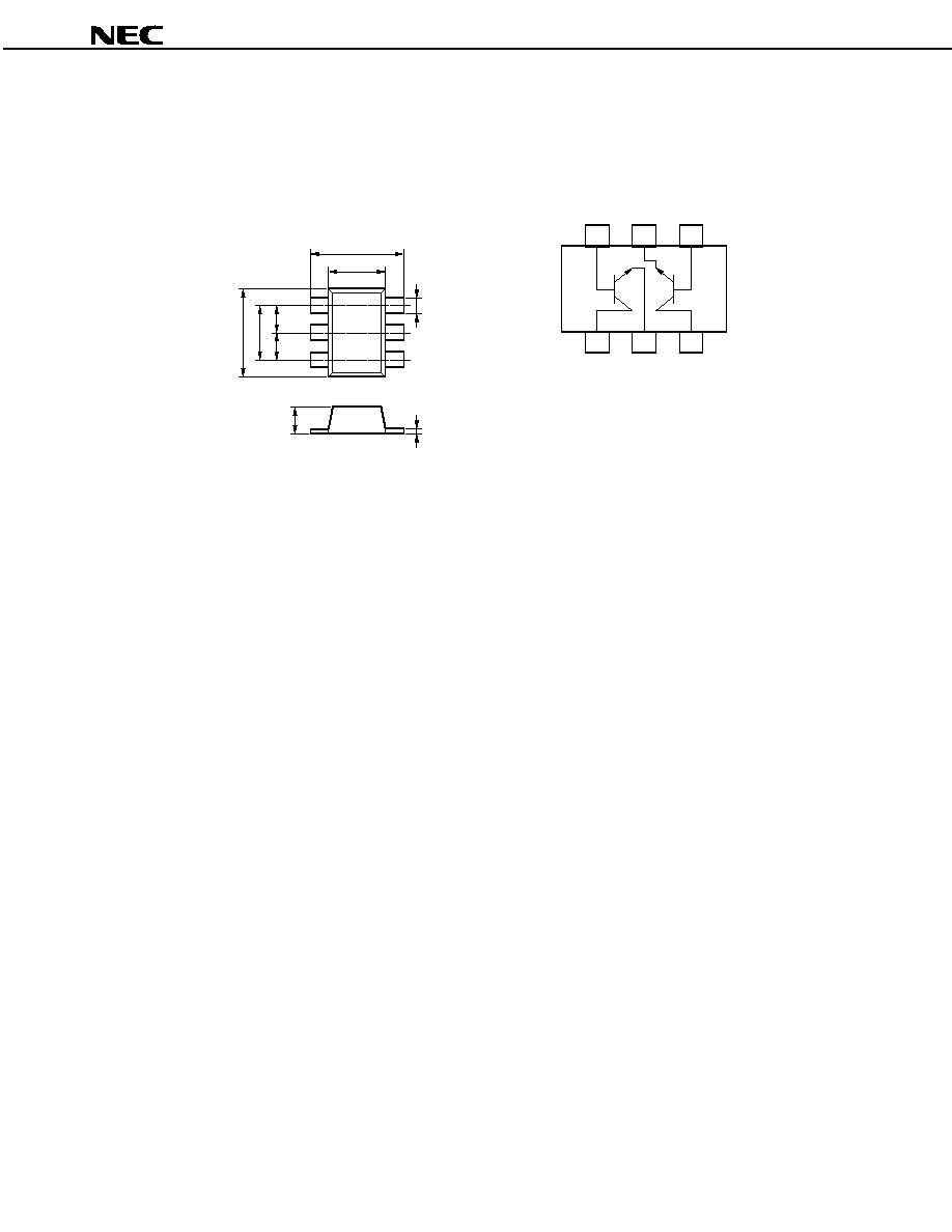
PACKAGE DIMENSIONS
FLAT-LEAD 6 PIN THIN-TYPE ULTRA SUPER MINIMOLD (UNIT: mm)
B1
6
C1
1
E2
5
E1
2
B2
C2
3
(Top View)
PIN CONNECTIONS
1. Collector (Q1)
2. Emitter (Q1)
3. Collector (Q2)
4. Base (Q2)
5. Emitter (Q2)
6. Base (Q1)
1
2
3
6
5
4
37
1.50±0.1
1.10±0.1
1.50±0.1
0.96
0.48
0.48
0.55±0.05
0.11
+0.1 ≠0.05
0.20
+0.1 ≠0.05
Q1
Q2
4

µ
µ
µ
µ
PA835TC
∑
The information in this document is subject to change without notice. Before using this document, please
confirm that this is the latest version.
∑
No part of this document may be copied or reproduced in any form or by any means without the prior written
consent of NEC Corporation. NEC Corporation assumes no responsibility for any errors which may appear in
this document.
∑
NEC Corporation does not assume any liability for infringement of patents, copyrights or other intellectual property
rights of third parties by or arising from use of a device described herein or any other liability arising from use
of such device. No license, either express, implied or otherwise, is granted under any patents, copyrights or other
intellectual property rights of NEC Corporation or others.
∑
Descriptions of circuits, software, and other related information in this document are provided for illustrative
purposes in semiconductor product operation and application examples. The incorporation of these circuits,
software, and information in the design of the customer's equipment shall be done under the full responsibility
of the customer. NEC Corporation assumes no responsibility for any losses incurred by the customer or third
parties arising from the use of these circuits, software, and information.
∑
While NEC Corporation has been making continuous effort to enhance the reliability of its semiconductor devices,
the possibility of defects cannot be eliminated entirely. To minimize risks of damage or injury to persons or
property arising from a defect in an NEC semiconductor device, customers must incorporate sufficient safety
measures in its design, such as redundancy, fire-containment, and anti-failure features.
∑
NEC devices are classified into the following three quality grades:
"Standard", "Special", and "Specific". The Specific quality grade applies only to devices developed based on a
customer designated "quality assurance program" for a specific application. The recommended applications of
a device depend on its quality grade, as indicated below. Customers must check the quality grade of each device
before using it in a particular application.
Standard: Computers, office equipment, communications equipment, test and measurement equipment,
audio and visual equipment, home electronic appliances, machine tools, personal electronic
equipment and industrial robots
Special: Transportation equipment (automobiles, trains, ships, etc.), traffic control systems, anti-disaster
systems, anti-crime systems, safety equipment and medical equipment (not specifically designed
for life support)
Specific: Aircraft, aerospace equipment, submersible repeaters, nuclear reactor control systems, life
support systems or medical equipment for life support, etc.
The quality grade of NEC devices is "Standard" unless otherwise specified in NEC's Data Sheets or Data Books.
If customers intend to use NEC devices for applications other than those specified for Standard quality grade,
they should contact an NEC sales representative in advance.
M7 98. 8