Caution: Electro-static sensitive devices
BIPOLAR DIGITAL INTEGRATED CIRCUITS
P
P
P
P
PB1506GV,
P
P
P
P
PB1507GV
3GHz INPUT DIVIDE BY 256, 128, 64 PRESCALER IC
FOR ANALOG DBS TUNERS
1996
©
Document No. P10767EJ3V0DS00 (3rd edition)
Date Published January 1998 N CP(K)
Printed in Japan
DATA SHEET
The
P
PB1506GV and
P
PB1507GV are 3.0 GHz input, high division silicon prescaler ICs for analog DBS tuner
applications. These ICs divide-by-256, 128 and 64 contribute to produce analog DBS tuners with kit-use of 17 K
series DTS controller or standard CMOS PLL synthesizer IC. The
P
PB1506GV/
P
PB1507GV are shrink package
versions of the
P
PB586G/588G or
P
PB1505GR so that these smaller packages contribute to reduce the mounting
space replacing from conventional ICs.
The
P
PB1506GV and
P
PB1507GV are manufactured using NEC's high f
T
NESATTMIV silicon bipolar process.
This process uses silicon nitride passivation film and gold electrodes. These materials can protect chip surface from
external pollution and prevent corrosion/migration. Thus, these ICs have excellent performance, uniformity and
reliability.
FEATURES
x
High toggle frequency
: f
in
= 0.5 GHz to 3.0 GHz
x
High-density surface mounting : 8-pin plastic SSOP (175 mil)
x
Low current consumption
: 5 V, 19 mA
x
Selectable high division
:
y
256,
y
128,
y
64
x
Pin connection variation
:
P
PB1506GV and
P
PB1507GV
APPLICATION
These ICs can use as a prescaler between local oscillator and PLL frequency synthesizer included modulus
prescaler. For example, following application can be chosen;
x
Analog DBS tuner's synthesizer
x
Analog CATV converter synthesizer
ORDERING INFORMATION
PART NUMBER
PACKAGE
MARKING
SUPPLYING FORM
P
PB1506GV-E1
8-pin plastic
1506
Embossed tape 8 mm wide. Pin 1 is in tape pull-out
P
PB1507GV-E1
SSOP (175 mil)
1507
direction. 1 000 p/reel.
Remarks To order evaluation samples, please contact your local NEC sales office.
(Part number for sample order:
P
PB1506GV,
P
PB1507GV)
2
P
P
P
P
PB1506GV,
P
P
P
P
PB1507GV
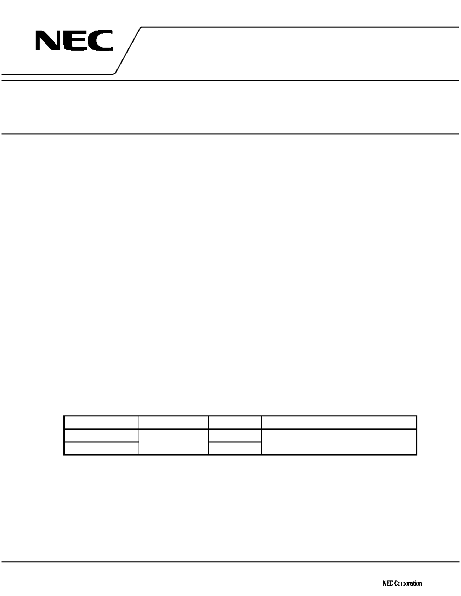
PIN CONNECTION (Top View)
Pin
NO.
P
PB1506GV
P
PB1507GV
1
SW1
IN
2
IN
V
CC
3
IN
SW1
4
GND
OUT
5
NC
GND
6
SW2
SW2
7
OUT
NC
8
V
CC
IN
PRODUCT LINE-UP
Features
(division, Freq.)
Part No.
I
CC
(mA)
f
in
(GHz)
V
CC
(V)
Package
Pin connection
y
512,
y
256, 2.5 GHz
P
PB586G
28
0.5 to 2.5
4.5 to 5.5
8 pin SOP 225 mil
NEC original
y
128,
y
64, 2.5 GHz
P
PB588G
26
0.5 to 2.5
4.5 to 5.5
y
256,
y
128,
y
64
P
PB1505GR
14
0.5 to 3.0
4.5 to 5.5
Standard
3.0 GHz
P
PB1506GV
19
0.5 to 3.0
4.5 to 5.5
8 pin SSOP 175 mil
NEC original
P
PB1507GV
19
0.5 to 3.0
4.5 to 5.5
Standard
Remarks
x
This table shows the TYP values of main parameters. Please refer to ELECTRICAL
CHARACTERISTICS.
x
P
PB586G and
P
PB588G are discontinued.
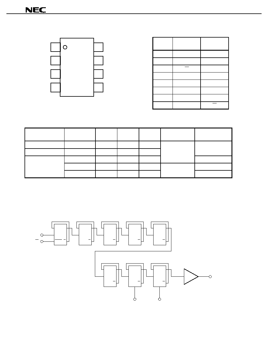
INTERNAL BLOCK DIAGRAM
D
CLK
CLK
Q
Q
D
CLK
Q
Q
D
CLK
Q
Q
D
CLK
Q
Q
D
CLK
Q
Q
D
CLK
Q
Q
D
CLK
Q
Q
D
CLK
Q
Q
SW1
SW2
AMP
OUT
IN
IN
5
6
7
8
4
3
2
1
3
P
P
P
P
PB1506GV,
P
P
P
P
PB1507GV
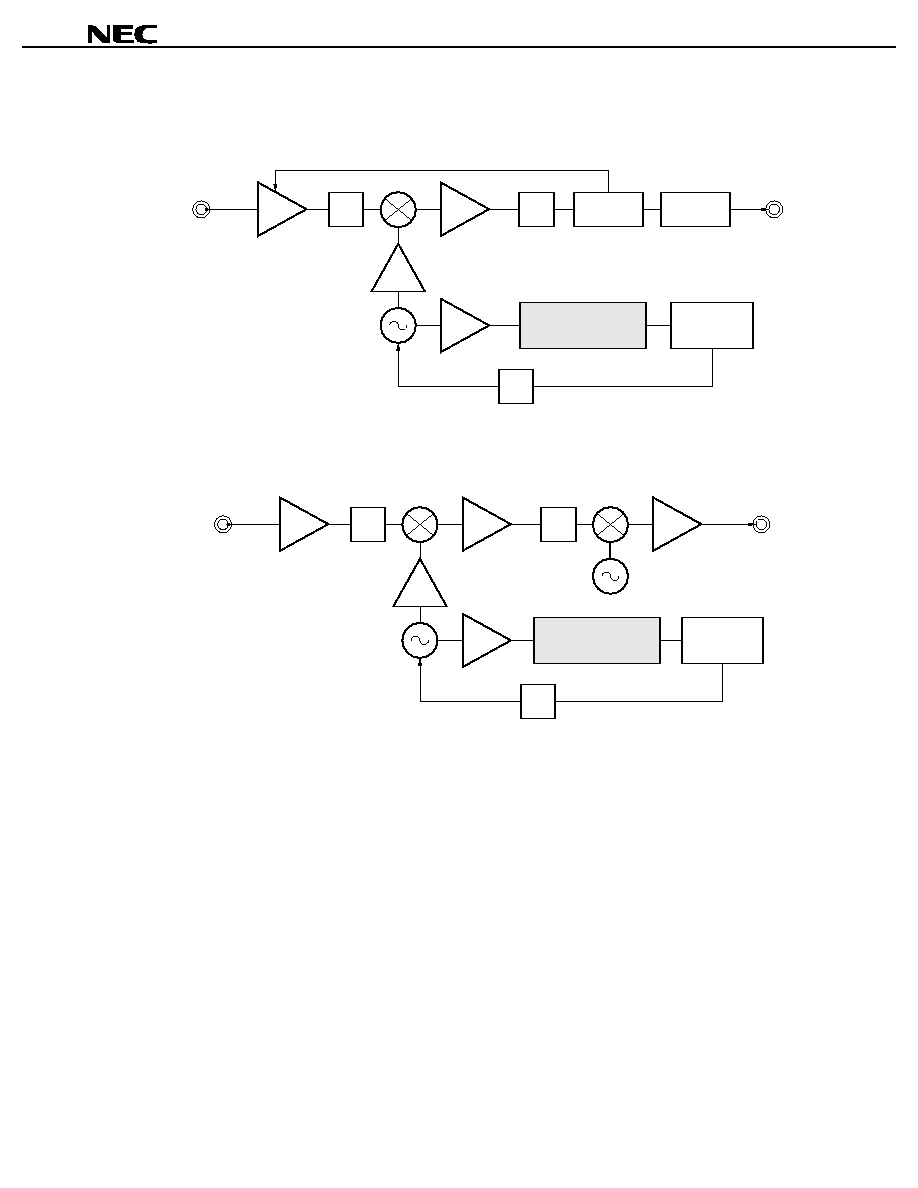
SYSTEM APPLICATION EXAMPLE
RF unit block of Analog DBS tuners
CMOS
PLL
synthesizer
BPF
SAW
AGC amp.
FM demo.
LPF
OSC
MIX
Baseband output
High division prescaler
PB1506GV or
PB1507GV
µ
µ
To 2150 MHz
To 2650 MHz
loop filter
1stIF input
from DBS converter
RF unit block of Analog CATV converter
CMOS
PLL
synthesizer
BPF
BPF
LPF
OSC
upconverter
To 800 MHz
To 2000 MHz
loop filter
To 1300 MHz
downconverter
High division prescaler
PB1506GV or
PB1507GV
µ
µ
4
P
P
P
P
PB1506GV,
P
P
P
P
PB1507GV
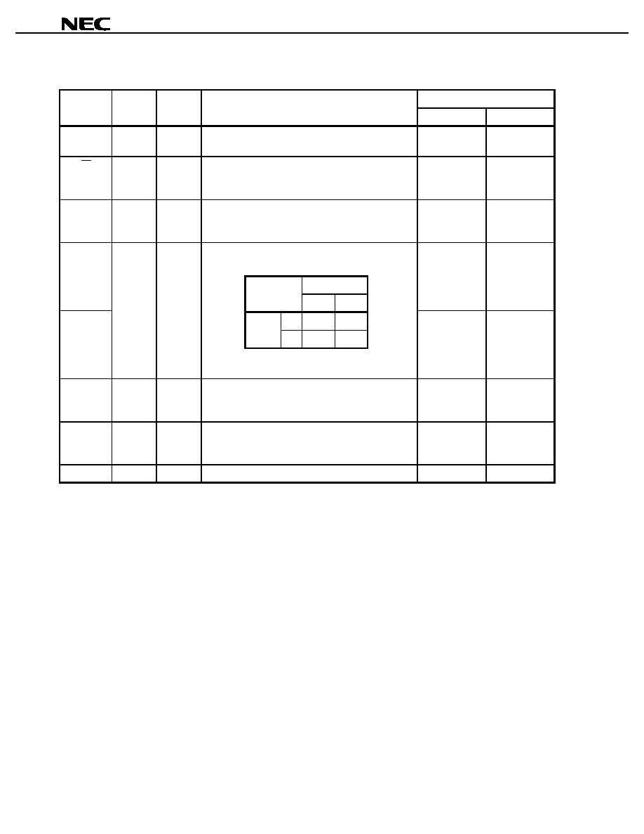
PIN EXPLANATION
Pin no.
P
PB1506GV
P
PB1507GV
IN
∑
2.9
Signal input pin. This pin should be coupled to signal
source with capacitor (e.g. 1 000 pF) for DC cut.
2
1
IN
∑
2.9
Signal input bypass pin. This pin must be equipped
with bypass capacitor (e.g. 1 000 pF) to minimize
ground impedance.
3
8
GND
0
∑
Ground pin. Ground pattern on the board should be
formed as wide as possible to minimize ground
impedance.
4
5
SW1
H/L
∑
Divide ratio input pin. The ratio can be determined by
following applied level to these pins.
1
3
SW2
These pins should be equipped with bypass capacitor
(e.g. 1 000 pF) to minimize ground impedance.
6
6
V
CC
4.5 to 5.5
∑
Power supply pin. This pin must be equipped with
bypass capacitor (e.g. 10 000 pF) to minimize ground
impedance.
8
2
OUT
∑
2.6 to 4.7
Divided frequency output pin. This pin is designed as
emitter follower output. This pin can be connected to
CMOS input due to 1.2 V
P-P
MIN output.
7
4
NC
∑
∑
Non connection pin. This pin must be openned.
5
7
SW1
Applied
voltage
V
Pin
voltage
V
Pin name
Functions and explanation
SW2
H
L
H
y
64
y
128
L
y
128
y
256
5
P
P
P
P
PB1506GV,
P
P
P
P
PB1507GV
ABSOLUTE MAXIMUM RATINGS
PARAMETER
SYMBOL
CONDITION
RATINGS
UNIT
Supply voltage
V
CC
T
A
= +25
q
C
0.5 to +6.0
V
Input voltage
V
in
T
A
= +25
q
C
0.5 to V
CC
+ 0.5
V
Total power dissipation
P
D
Mounted on double sided copper clad
50
u
50
u
1.6 mm epoxy glass PWB (T
A
=
+85
q
C)
250
mW
Operating ambient temperature
T
A
40 to +85
q
C
Storage temperature
T
stg
55 to +150
q
C
RECOMMENDED OPERATING CONDITIONS
PARAMETER
SYMBOL
MIN.
TYP.
MAX.
UNIT
NOTICE
Supply voltage
V
CC
4.5
5.0
5.5
V
Operating ambient temperature
T
A
40
+25
+85
q
C
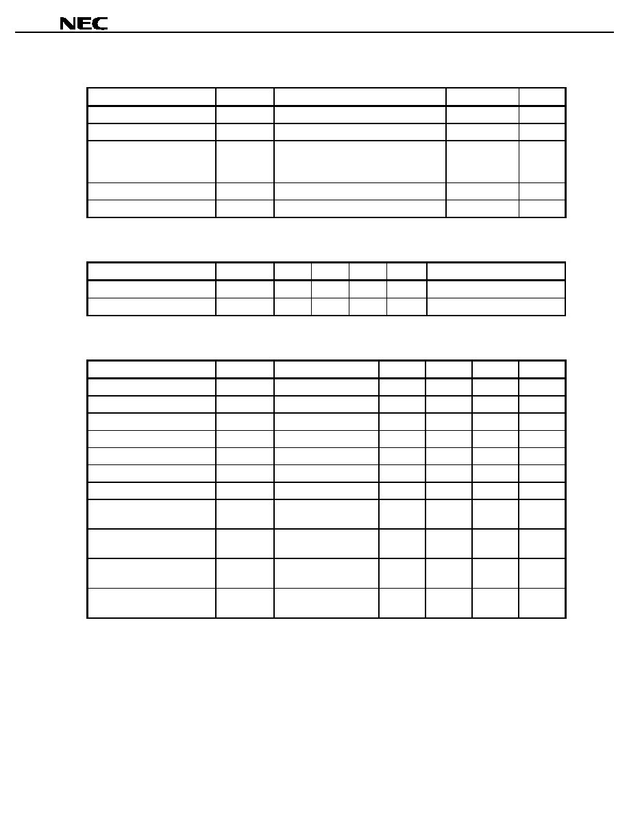
ELECTRICAL CHARACTERISTICS (T
A
=
40 to +85
q
q
q
q
C, V
CC
= 4.5 to 5.5 V, Z
S
= 50
:
:
:
:
)
PARAMETER
SYMBOL
TEST CONDITION
MIN.
TYP.
MAX.
UNIT
Circuit current
I
CC
No signals
12.5
19
26.5
mA
Upper limit operating frequency
f
in(u)
P
in
=
15 to +6 dBm
3.0
∑
∑
GHz
Lower limit operating frequency 1
f
in(L)1
P
in
=
10 to +6 dBm
∑
∑
0.5
GHz
Lower limit operating frequency 2
f
in(L)2
P
in
=
15 to +6 dBm
∑
∑
1.0
GHz
Input power 1
P
in1
f
in
= 1.0 to 3.0 GHz
15
∑
+6
dBm
Input power 2
P
in2
f
in
= 0.5 to 1.0 GHz
10
∑
+6
dBm
Output Voltage
V
out
C
L
= 8 pF
1.2
1.6
∑
V
P-P
Divide ratio control input high
V
IH1
Connection in the test
circuit
V
CC
V
CC
V
CC
Divide ratio control input low
V
IL1
Connection in the test
circuit
OPEN or
GND
OPEN or
GND
OPEN or
GND
Divide ratio control input high
V
IH2
Connection in the test
circuit
V
CC
V
CC
V
CC
Divide ratio control input low
V
IL2
Connection in the test
circuit
OPEN or
GND
OPEN or
GND
OPEN or
GND