 | –≠–Ľ–Ķ–ļ—ā—Ä–ĺ–Ĺ–Ĺ—č–Ļ –ļ–ĺ–ľ–Ņ–ĺ–Ĺ–Ķ–Ĺ—ā: UPB1508GV | –°–ļ–į—á–į—ā—Ć:  PDF PDF  ZIP ZIP |
BIPOLAR DIGITAL INTEGRATED CIRCUIT
Ķ
Ķ
Ķ
Ķ
PB1508GV
3 GHz INPUT DIVIDE BY 2 PRESCALER IC
FOR DBS TUNERS
1996
©
Document No. P10768EJ2V0DS00 (2nd edition)
Date Published September 1997 N
Printed in Japan
DATA SHEET
Ķ
PB1508GV is a 3.0 GHz input divide by 2 prescaler IC for DBS tuner applications.
Ķ
PB1508GV can make
VHF/UHF band PLL frequency synthesizer apply to DBS/ECS tuners.
Ķ
PB1508GV is a shrink package version of
Ķ
PB584G so that this small package contributes to reduce the mounting space.
Ķ
PB1508GV is manufactured using NEC's high f
T
NESATTM IV silicon bipolar process. This process uses silicon
nitride passivation film and gold electrodes. These materials can protect chip surface from external pollution and
prevent corrosion/migration. Thus, this IC has excellent performance, uniformity and reliability.
FEATURES
∑
High toggle frequency
: f
in
= 0.5 GHz to 3.0 GHz
∑
High-density surface mounting : 8 pin plastic SSOP (175 mil)
∑
Low current consumption
: 5 V, 12 mA
∑
Fixed division
:
ų
2
APPLICATION
∑
Prescaler between local oscillator and PLL frequency synthesizer included modulus prescaler
∑
DBS tuners with kit use of VHF/UHF band PLL frequency synthesizer
ORDERING INFORMATION
PART NUMBER
PACKAGE
MARKING
SUPPLYING FORM
Ķ
PB1508GV-E1
8 pin plastic SSOP
(175 mil)
1508
Embossed tape 8 mm wide. Pin 1 is in tape pull-out
direction. 1 000 p/reel.
Remarks To order evaluation samples, please contact your local NEC sales office.
(Part number for sample order:
Ķ
PB1508GV)
Caution: Electro-static sensitive devices
2
Ķ
Ķ
Ķ
Ķ
PB1508GV
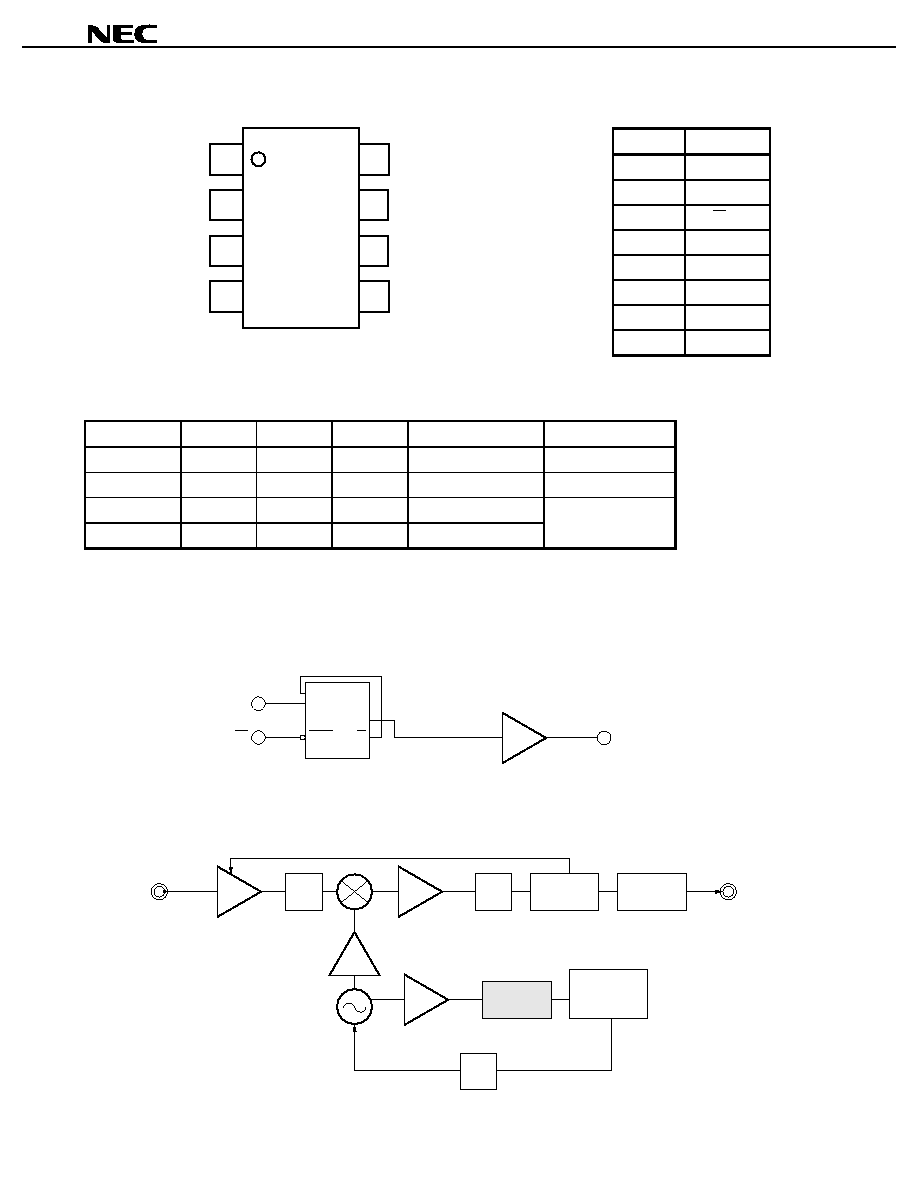
PIN CONNECTION (Top View)
Pin No.
Pin name
1
V
CC
2
IN
3
IN
4
GND
5
GND
6
NC
7
OUT
8
NC
PRODUCT LINE-UP
Product No.
I
CC
(mA)
f
in
(GHz)
V
CC
(V)
Package
Pin Connection
Ķ
PB581A
30
0.5 to 2.8
4.5 to 5.5
8 pins CAN
≠
Ķ
PB581C
30
0.5 to 2.2
4.5 to 5.5
8 pins DIP (300 mil)
NEC Original
Ķ
PB584G
18
0.5 to 2.5
4.5 to 5.5
8 pins SOP (225 mil)
NEC Original
Ķ
PB1508GV
12
0.5 to 3.0
4.5 to 5.5
8 pins SSOP (175 mil)
Remarks This table shows the TYP values of main parameters. Please refer to ELECTRICAL
CHARACTERISTICS.
Ķ
PB581A,
Ķ
PB581C and
Ķ
PB584G are discontinued.
INTERNAL BLOCK DIAGRAM
IN
IN
CLK
CLK
D
Q
Q
OUT
AMP
SYSTEM APPLICATION EXAMPLE
RF unit block of DBS tuners
1stIF input
from DBS converter
MIX
BPF
OSC
LPF
PB1508GV
Ķ
ų 2
Prescaler
PLLsynth.
for VHF/UHF
band
SAW
AGC amp.
FM demo.
Baseband output
1
2
3
4
8
7
6
5
3
Ķ
Ķ
Ķ
Ķ
PB1508GV
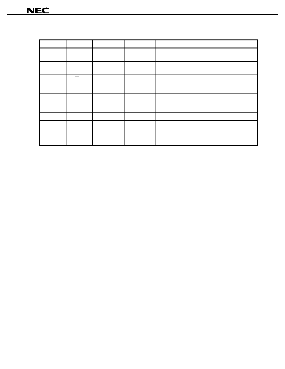
PIN EXPLANATION
Pin No.
Symbol
Applied voltage
PIN voltage
Functions and explanation
1
V
CC
4.5 to 5.5
Power supply pin. This pin must be equipped with bypass
capacitor (eg 1 000 pF) to minimize ground impedance.
2
IN
1.7 to 4.95
Signal input pin. This pin should be coupled to signal
source with capacitor (eg 1 000 pF) for DC cut.
3
IN
1.7 to 4.95
Signal input bypass pin. This pin must be equipped with
bypass capacitor (eg 1 000 pF) to minimize ground
impedance.
4, 5
GND
0
Ground pin. Ground pattern on the board should be
formed as wide as possible to minimize ground
impedance.
6, 8
NC
Non connection pins. These pins should be opened.
7
OUT
1.0 to 4.7
Divided frequency output pin. This pin is designed as
emitter follower output. This pin can be connected to
input of prescaler within PLL synthesizer through DC cut
capacitor.

4
Ķ
Ķ
Ķ
Ķ
PB1508GV
ABSOLUTE MAXIMUM RATINGS
PARAMETER
SYMBOL
CONDITION
RATINGS
UNIT
Supply voltage
V
CC
T
A
= +25
į
C
6.0
V
Input voltage
V
in
T
A
= +25
į
C
6.0
V
Total power dissipation
P
D
Mounted on double sided copper clad
50
◊
50
◊
1.6 mm epoxy glass PWB (T
A
= +85
į
C)
250
mW
Operating ambient temperature
T
A
-
40 to +85
į
C
Storage temperature
T
stg
-
55 to +150
į
C
RECOMMENDED OPERATING CONDITIONS
PARAMETER
SYMBOL
MIN.
TYP.
MAX.
UNIT
REMARKS
Supply voltage
V
CC
4.5
5.0
5.5
V
Operating ambient temperature
T
A
-
40
+25
+85
į
C
ELECTRICAL CHARACTERISTICS (T
A
=
-
-
-
-
40 to +85
į
į
į
į
C, V
CC
= 4.5 to 5.5 V, Z
S
= Z
L
= 50
)
PARAMETER
SYMBOL
TEST CONDITION
MIN.
TYP.
MAX.
UNIT
Circuit current
I
CC
No signals
7.6
12
14.5
mA
Upper limit operating frequency 1
f
in(U)1
P
in
=
-
10 to +6 dBm
3.0
GHz
Upper limit operating frequency 2
f
in(U)2
P
in
=
-
15 to +6 dBm
2.7
GHz
Lower limit operating frequency
f
in(L)
P
in
=
-
15 to +6 dBm
0.5
GHz
Input power 1
P
in1
f
in
= 2.7 to 3.0 GHz
-
10
+6
dBm
Input power 2
P
in2
f
in
= 0.5 to 2.7 GHz
-
15
+6
dBm
Output power
P
out
P
in
= 0 dBm, f
in
= 2 GHz
-
12
-
7
dBm

5
Ķ
Ķ
Ķ
Ķ
PB1508GV
TYPICAL CHARACTERISTICS (unless otherwise specified T
A
= +25įC)
15
10
5
0
0
1
2
3
V
CC
- Supply Voltage - V
I
CC
- Circuit Current - mA
4
5
6
CIRCUIT CURRENT vs. SUPPLY VOLTAGE
No signals
T
A
= +85 įC
T
A
= +25 įC
T
A
= ≠40 įC
+20
+10
0
≠10
≠20
≠30
≠40
≠50
≠60
100
1000
4000
f
in
- Input Frequency - MHz
P
in
- Input Power - dBm
P
in
- Input Power - dBm
P
out
- Output Power - dBm
P
out
- Output Power - dBm
INPUT POWER vs. INPUT FREQUENCY
+20
+10
0
≠10
≠20
≠30
≠40
≠50
≠60
100
1000
4000
f
in
-Input Frequency - MHz
f
in
- Input Frequency - MHz
f
in
-Input Frequency - MHz
INPUT POWER vs. INPUT FREQUENCY
OUTPUT POWER vs. INPUT FREQUENCY
OUTPUT POWER vs. INPUT FREQUENCY
0
≠2
≠4
≠6
≠8
≠10
≠12
≠14
≠16
0
≠2
≠4
≠6
≠8
≠10
≠12
≠14
≠16
100
1000
4000
100
1000
4000
T
A
= +25 įC
V
CC
= 5.0 V
P
in
= 0 dBm
Z
L
= 50
T
A
= +25 įC
P
in
= 0 dBm
Z
L
= 50
V
CC
= 4.5 to 5.5 V
V
CC
= 4.5 to 5.5 V
V
CC
= 4.5 to 5.5 V
T
A
= ≠40 įC
T
A
= ≠40 įC
T
A
= +25 įC
T
A
= +25 įC
T
A
= +85 įC
T
A
= +85 įC
V
CC
= 4.5 V
V
CC
= 5.0 V
V
CC
= 5.5 V
T
A
= ≠40 įC
T
A
= ≠40 įC
T
A
= +25 įC
T
A
= +25 įC
T
A
= +85 įC
T
A
= +85 įC
Guaranteed
Operating
Window
Guaranteed
Operating
Window