 | –≠–ª–µ–∫—Ç—Ä–æ–Ω–Ω—ã–π –∫–æ–º–ø–æ–Ω–µ–Ω—Ç: UPC1658G | –°–∫–∞—á–∞—Ç—å:  PDF PDF  ZIP ZIP |

Caution Electro-static sensitive devices
The information in this document is subject to change without notice. Before using this document, please
confirm that this is the latest version.
Not all devices/types available in every country. Please check with local NEC representative for
availability and additional information.
BIPOLAR ANALOG INTEGRATED CIRCUIT
µ
µ
µ
µ
PC1658G
LOW NOISE, HIGH FREQUENCY Si MMIC AMPLIFIER
Document No. P11120EJ3V0DS00 (3rd edition)
Date Published September 1999 N CP(K)
Printed in Japan
DATA SHEET
The mark
shows major revised points.
1996, 1999
©
DESCRIPTION
The
µ
PC1658G is a silicon monolithic integrated circuit designed as amplifier for high frequency system
applications. Bandwidth and output power level can be determined according to external resistor constants of
negative feedback and final stage collector. This IC is available in 8-pin plastic SOP.
This IC is manufactured using NEC's 10 GHz f
T
NESAT
TM
II silicon bipolar process. This process uses silicon
nitride passivation film and gold electrodes. These materials can protect chip surface from external pollution and
prevent corrosion/migration. Thus, this IC has excellent performance, uniformity and reliability.
FEATURES
∑
Low noise figure
: NF
3 dB
∑
Due to the external negative feedback circuit, the power gain can be adjustable by selecting appropriate
resistance constants.
: G
P
40 dB @ Without negative feedback resistor
: G
P
18 dB @ With negative feedback resistor
∑
Wideband response
: f
3dB
= 1.0 GHz @ G
P
= 18 dB
∑
External resistor can vary the collector current of the final transistor in the IC to adjust the saturated output level.
APPLICATIONS
∑
IF buffer amplifier of high frequency system
∑
Measurement equipment
ORDERING INFORMATION
Part Number
Package
Marking
Supplying Form
µ
PC1658G-E1
8-pin plastic SOP (225 mil)
1658
Embossed tape 12 mm wide.
1 pin is tape pull-out direction.
Qty 2.5 kp/reel.
Remark To order evaluation samples, please contact your local NEC sales office.
(Part number for sample order:
µ
PC1658G)
Caution TO-99 CAN package (
µ
µ
µ
µ
PC1658A) and 8-pin plastic DIP package (
µ
µ
µ
µ
PC1658C) products are
discontinued.
Data Sheet P11120EJ3V0DS00
2
µ
µ
µ
µ
PC1658G
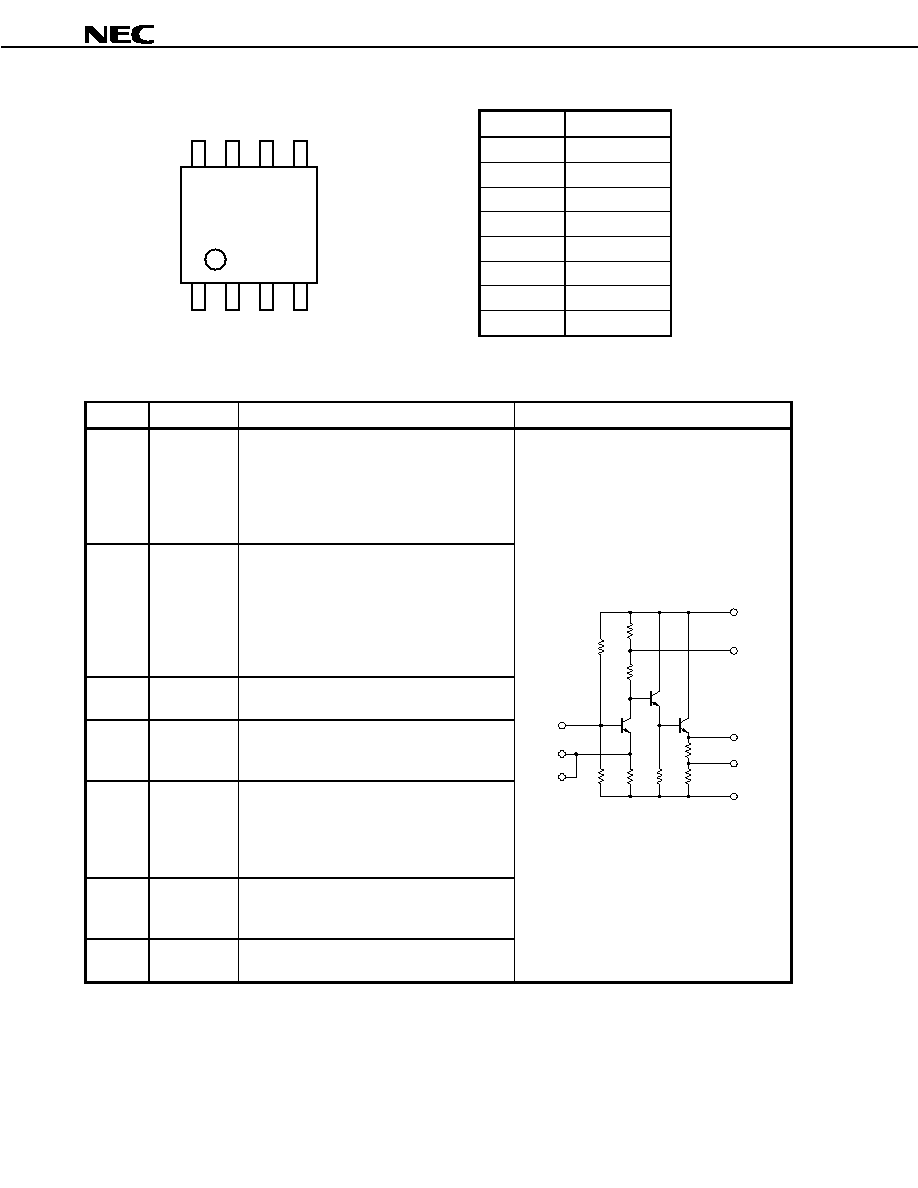
PIN CONNECTIONS
PIN EXPLANATION
Pin No.
Pin Name
Function and Applications
Internal Equivalent Circuit
1
GND
Ground pin. This pin should be connected to
system ground with minimum inductance.
Ground pattern on the board should be formed
as possible. All the ground pins must be
connected together with wide ground pattern to
decrease impedance difference.
2
Test Point
Test Point pin. The collector current of Q
2
and
Q
3
can be varied by connecting an appropriate
external resistance between this pin and GND
or by shorting this pin to GND. By increasing
the collector current of Q
3
, the output level
improves and the IC can operate as a low-
distortion amplifier.
3
Output
Signal output pin. This pin must be coupled to
signal source with capacitor for DC cut.
4
V
CC
Power supply pin. This pin should be externally
equipped with bypass capacitor to minimize its
impedance.
5
Test Point
By connecting this pin to the power supply
through an appropriate external resistance or by
shorting this pin directly to the power supply,
the gain can be adjustable (when using pin 2,
short the pin 5 to the power supply).
6
Input
Signal input pin. Through negative feedback
from output pin with an external circuit, the IC
operates as a wideband amplifier.
7
8
Bypass
Emitter bypass pins of Q
1
. Bypass these pins
to GND with a capacitor.
Q1
Q3
Q2
R4
R3
R1
6
7
8
Input
Bypass
Bypass
R2
R5
R6
R8
R7
3
2
1
Output
Test point
GND
5 Test point
4 V
CC
Pin No.
Pin Name
1
GND
2
Test Point
3
Output
4
V
CC
5
Test Point
6
Input
7
Bypass
8
Bypass
8
7
6
5
1
2
3
(Top View)
4

Data Sheet P11120EJ3V0DS00
3
µ
µ
µ
µ
PC1658G
ABSOLUTE MAXIMUM RATINGS
Parameter
Symbol
Conditions
Rating
Unit
Supply Voltage
V
CC
T
A
= +25 ∞C
12
V
Output Transistor Current
I
Q3
T
A
= +25 ∞C
40
mA
Power Dissipation
P
D
Mounted on double copper clad 50
◊
50
◊
1.6 mm
epoxy glass PWB (T
A
= +70
∞
C)
280
mW
Operating Ambient Temperature
T
A
≠40 to +75
∞C
Storage Temperature
T
stg
≠55 to +150
∞C
ELECTRICAL CHARACTERISTICS (T
A
= +25
∞
∞
∞
∞
C, V
CC
= 10.0 V, Z
S
= Z
L
= 50
, Test circuit 1)
Parameter
Symbol
Conditions
MIN.
TYP.
MAX.
Unit
Circuit Current
I
CC
No signal
9
-
18
mA
Power Gain 1
G
P1
f = 10 MHz
37
41
45
dB
Power Gain 2
G
P2
f = 100 MHz
28
31
34
dB
Power Gain 3
G
P3
f = 500 MHz
14
17
20
dB
Noise Figure 1
NF
1
f = 100 MHz
-
1.5
2.5
dB
Noise Figure 2
NF
2
f = 500 MHz
-
2.0
3.0
dB
TEST SET-UP
Signal Generator
INPUT
0.01 F
µ
Power Supply
Test Circuit
1 to 3
Z
S
= 50
Z
L
= 50
OUTPUT
Spectrum Analyzer or
Network Analyzer

Data Sheet P11120EJ3V0DS00
4
µ
µ
µ
µ
PC1658G
TEST CIRCUITS
TEST CIRCUIT 1 (Low-noise amplifier)
TEST CIRCUIT 2 (Wideband low-noise amplifier)
TEST CIRCUIT 3 (Wideband low-noise amplifier with improved output level)
Output
0.01 F
Input
0.01 F
0.01 F
V
CC
0.1 F
µ
µ
µ
µ
Output
0.01 F
Input
0.01 F
µ
µ
µ
µ
µ
µ
µ
µ
µ
µ
0.01 F
V
CC
0.1 F
0.01 F
R
F
Output
Input
0.01 F
V
CC
0.1 F
0.01 F
220
0.01 F
0.01 F
8
7
6
5
1
2
3
4
8
7
6
5
1
2
3
4
8
7
6
5
1
2
3
4
180

Data Sheet P11120EJ3V0DS00
5
µ
µ
µ
µ
PC1658G
ILLUSTRATION OF THE TEST CIRCUIT ASSEMBLED ON EVALUATION BOARD
C1
GND
C3
C4
C2
R1
OUT
V
CC
IN
1
PC1658G
µ
Notes 1. 50
◊
50
◊
0.4 mm double sided copper clad polyimide board.
2. Back side: GND pattern
3. Solder plated on pattern
4. : Through holes
COMPONENT LIST
Value
Remarks
C1 to C3
0.01
µ
F
C4
0.1
µ
F
Necessary to all the test circuits
Open
Note
In the case of Low-noise Amplifier
R1
180
In the case of Wideband Low-noise Amplifier with improved output level
Note In the case of Low-noise Amplifier, R1 is not mounted.