
Caution Electro-static sensitive devices
The information in this document is subject to change without notice. Before using this document, please
confirm that this is the latest version.
Not all devices/types available in every country. Please check with local NEC representative for
availability and additional information.
BIPOLAR ANALOG INTEGRATED CIRCUIT
µ
µ
µ
µ
PC1663
DC to VHF WIDEBAND DIFFERENTIAL INPUT AND OUTPUT AMPLIFIER IC
DATA SHEET
Document No. G11024EJ6V0DS00 (6th edition)
Date Published September 1999 N CP(K)
Printed in Japan
The mark
shows major revised points.
1987, 1999
©
DESCRIPTION
The
µ
PC1663 is a differential input, differential output wideband amplifier IC that uses an high frequency silicon
bipolar process. This process improves bandwidth phase characteristics, input noise voltage characteristics, and low
power consumption when compared to conventional HF-band differential amplifier ICs.
These features make this device suitable as a wideband amplifier in high-definition TVs, high-resolution monitors,
broadcasting satellite receivers, and video cameras, as a sense amplifier in high-density CCD and optical pick-up
products, or as a pulse amplifier for optical data links.
These ICs are manufactured using NEC's 6 GHz f
T
NESAT
TM
I silicon bipolar process. This process uses silicon
nitride passivation film and gold electrodes. These materials can protect chip surface from external pollution and
prevent corrosion/migration. Thus, these ICs have excellent performance, uniformity and reliability.
FEATURES
∑ Bandwidth and typical gain : 120 MHz @ A
VOL
= 300
700 MHz @ A
VOL
= 10
∑ Phase delay
: ≠85 deg. @ A
VOL
= 100, 100 MHz
∑ Input Noise Voltage
: 3
µ
V
r.m.s.
(R
S
= 50
, 10 k to 10 MHz)
∑ Supply Current
: 13mA TYP. @ V
CC
±
=
±
6 V
∑ Gain adjustable from 10 to 300 with external resistor
∑ No frequency compensation required (Small phase delay at 10 MHz or less)
ORDERING INFORMATION
Part Number
Package
Marking
Supplying Form
µ
PC1663G-E1
8-pin plastic SOP (225 mil)
Embossed tape 12 mm wide.
Pin 1 is in tape pull-out direction.
Qty 2.5 kp/reel.
µ
PC1663GV-E1
8-pin plastic SSOP (175 mil)
1663
Embossed tape 8 mm wide.
Pin 1 is in tape pull-out direction.
Qty 1 kp/reel.
Remark To order evaluation samples, please contact your local NEC sales office. (Part number for sample order:
µ
PC1663G,
µ
PC1663GV)
Caution
µ
µ
µ
µ
PC1663C (8-pin plastic DIP) is discontinued.

Data Sheet G11024EJ6V0DS00
2
µ
µ
µ
µ
PC1663
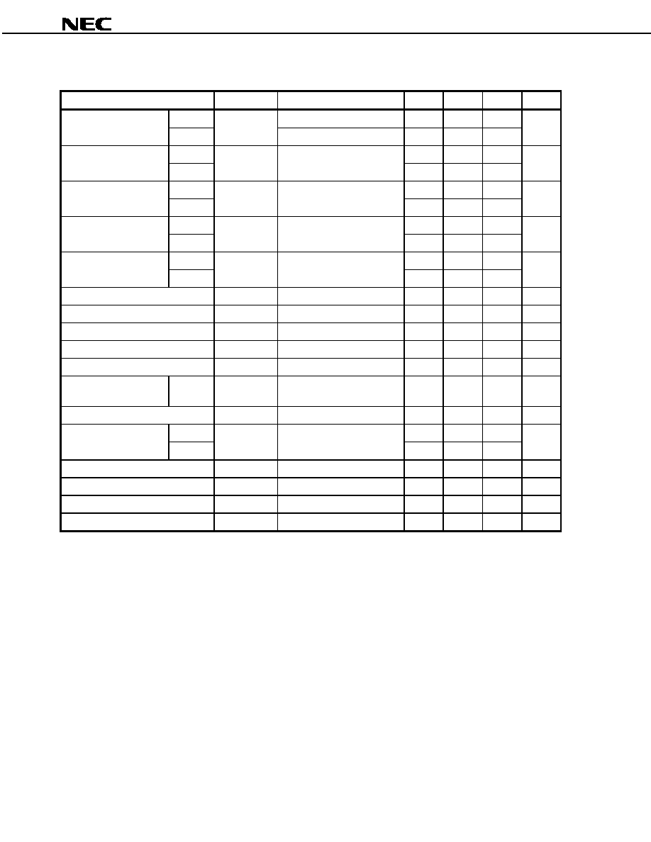
CONNECTION DIAGRAM
PIN EXPLANATIONS
Pin
No.
Pin
Name
In Dual
Bias
(V)
In Single
Bias
(V)
Functions and Applications
Internal Equivalent Circuit
8
1
IN
1
IN
2
Pin
voltage
0
Apply
voltage
V
CC
/2
Input pin
5
4
OUT
1
OUT
2
Pin
voltage
0
Apply
voltage
V
CC
/2
Output pin
6
V
CC
+
±
2 to
±
6.5
≠0.3 to +14
Plus voltage supply pin.
This pin should be
connected with bypass
capacitor to minimize AC
impedance.
3
V
CC
≠
GND
Minus voltage supply pin.
This pin should be
connected with bypass
capacitor to minimize AC
impedance.
7
2
G
1A
G
1B
--
--
Gain adjustment pin.
External resistor from 0 to
10 k
can be inserted
between pin 2 and 7 to
determine gain value.
(G
2A
)
(G
2B
)
Note
Note
8
1
7
2
6
5
4
3
Internal circuit constants should be referred to
application note.
Note
µ
PC1664 which had G
2A
, G
2B
of the other gain adjustment pins is discontinued.
Pin No.
Pin Name
1
IN
2
2
G
1B
3
V
CC
-
4
OUT
2
5
OUT
1
6
V
CC
+
7
G
1A
8
IN
1
8
7
6
5
1
(Top View)
2
3
4

Data Sheet G11024EJ6V0DS00
3
µ
µ
µ
µ
PC1663
ABSOLUTE MAXIMUM RATINGS (T
A
= +25 ∞C)
Parameter
Symbol
µ
PC1663G
µ
PC1663GV
Unit
Supply Voltage
V
CC
±
±
7
±
7
V
Power Dissipation
P
D
280 (T
A
= +75∞C)
Note
280 (T
A
= +75
∞
C)
Note
mW
Differential Input Voltage
V
ID
±
5
±
5
V
Input Voltage
V
ICM
±
6
(within V
CC
-
to V
CC
+
range)
±
6
(within V
CC
-
to V
CC
+
range)
V
Output Current
I
O
35
35
mA
Operating Ambient Temperature
T
A
-
45 to
+
75
-
45 to
+
75
∞C
Storage Temperature
T
stg
-
55 to
+
150
-
55 to
+
150
∞C
Note
Mounted on double sided copper clad 50
◊
50
◊
1.6 mm epoxy glass PWB
RECOMMENDED OPERATING CONDITIONS
Parameter
Symbol
MIN.
TYP.
MAX.
Unit
Supply Voltage
V
CC
±
±
2
±
6
±
6.5
V
Output Source Current
I
O source
--
--
20
mA
Output Sink Current
I
O sink
--
--
2.5
mA
Operating Frequency Range
f
opt
DC
--
200
MHz
Data Sheet G11024EJ6V0DS00
4
µ
µ
µ
µ
PC1663
ELECTRICAL CHARACTERISTICS (T
A
=
+
+
+
+
25 ∞C, V
CC
±
±
±
±
=
±
±
±
±
6 V)
Parameter
Symbol
Conditions
MIN.
TYP.
MAX.
Unit
Differential Voltage Gain
Gain 1
A
vd
f = 10 MHz
Note 1
200
320
500
--
Gain 2
f = 10 MHz
Note 2
8
10
12
Bandwidth
Gain 1
BW
R
S
= 50
(3 dB down point)
--
120
--
MHz
Gain 2
--
700
--
Rise Time
Gain 1
t
r
R
S
= 50
, V
out
= 1 V
P-P
--
2.9
--
ns
Gain 2
--
2.7
--
Propagation Delay
Gain 1
t
pd
R
S
= 50
, V
out
= 1 V
P-P
--
2
--
ns
Gain 2
--
1.2
--
Input Resistance
Gain 1
R
in
--
4.0
--
k
Gain 2
50
180
--
Input Capacitance
C
in
--
2
--
pF
Input Offset Current
I
IO
--
0.4
5.0
µ
A
Input Bias Current
I
B
--
20
40
µ
A
Input Noise Voltage
V
n
R
S
= 50
, 10 k to 10 MHz
--
3
--
µ
V
r.m.s.
Input Voltage Range
V
I
±
1.0
--
--
V
Common Mode
Rejection Ratio
Gain 2
CMR
V
cm
=
±
1 V, f
100 kHz
53
94
--
dB
Supply Voltage Rejection Ratio
SVR
V =
±
0.5 V
50
70
--
dB
Output Offset Voltage
Gain 1
V
O(off)
V
O(off)
= |OUT
1
≠ OUT
2
|
--
0.3
1.5
V
Gain 2
--
0.1
1.0
Output Common Mode Voltage
V
O(CM)
2.4
2.9
3.4
V
Output Voltage Swing
V
OP-P
Single-ended
3.0
4.0
--
V
P-P
Output Sink Current
I
sink
2.5
3.6
--
mA
Power Supply Current
I
CC
--
13
20
mA
Notes 1. Gain select pins G
1A
and G
1B
are connected.
2. All gain select pins are opened.
Data Sheet G11024EJ6V0DS00
5
µ
µ
µ
µ
PC1663
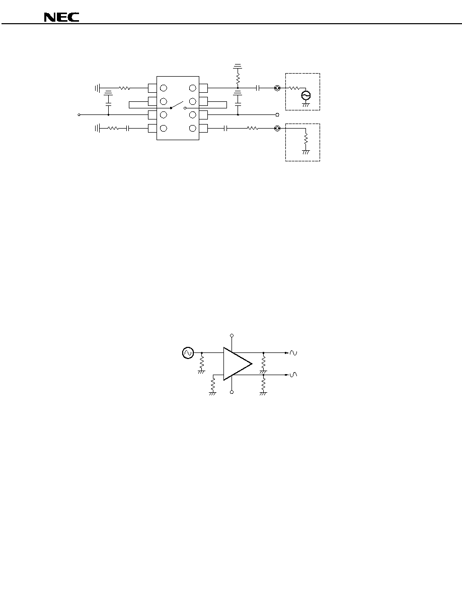
TEST CIRCUIT
50
1 000 pF
µ
µ
µ
1 k
V
CC
≠
0.1 F
1
2
3
4
8
7
6
5
50
IN
Z
S
= 50
Z
L
=
50
OUT
1 000 pF
950
0.1 F
0.1 F
V
CC
+
Remark Measurement value at
OUT connector should
be converced into DUT's
output value at pin 5.
Remark
Definition and test circuit of each characteristic should be referred to application note `Usage of
µ
PC1663 (Document No. G12290E)'.
NOTES ON CORRECT USE
(1)
Observe precautions for handling because of electro-static sensitive devices.
(2)
Form a ground pattern as wide as possible to minimize ground impedance (to prevent undesired
oscillation).
(3)
The bypass capacitor should be attached to V
CC
line.
(4)
When gain between Gain 1 and Gain 2 is necessary, insert adjustment resistor (0 to 10 k
) between
G
1A
and G
1B
to determine gain value.
(5)
Due to high-frequency characteristics, the physical circuit layout is very critical. Supply voltage line
bypass, double-sided printed-circuit board, and wide-area ground line layout are necessary for stable
operation. Two signal resistors connected to both inputs and two load resistors connected to both
outputs should be balanced for stable operation.
50
50
(150
to
)
(150
to
)
V
CC
+
V
CC
≠