
DATA SHEET
The information in this document is subject to change without notice. Before using this document, please
confirm that this is the latest version.
Not all devices/types available in every country. Please check with local NEC representative for
availability and additional information.
BIPOLAR ANALOG INTEGRATED CIRCUIT
µ
µ
µ
µ
PC1678G
5 V-BIAS, +17.5 dBm OUTPUT, 2.0 GHz WIDEBAND
Si MMIC AMPLIFIER
Document No. P11491EJ4V0DS00 (4th edition)
Date Published September 1999 N CP(K)
Printed in Japan
DATA SHEET
The mark
shows major revised points.
1996, 1999
©
DESCRIPTION
The
µ
PC1678G is a silicon monolithic integrated circuit designed as medium output power amplifier for high
frequency system applications. Due to +17.5 dBm TYP. output at 2 GHz, this IC is recommendable for transmitter
stage amplifier of L BAND wireless communication systems. This IC is packaged in 8-pin plastic SOP.
This IC is manufactured using NEC's 20 GHz f
T
NESATTMIV silicon bipolar process. This process uses silicon
nitride passivation film and gold electrodes. These materials can protect chip surface from external pollution and
prevent corrosion/migration. Thus, this IC has excellent performance, uniformity and reliability.
FEATURES
∑
Supply voltage
: V
CC
= 4.5 to 5.5 V
∑
Saturated output power
: P
O(sat)
= +17.5 dBm TYP. @ f = 500 MHz with external inductor
∑
Wideband response
: f
u
= 2.0 GHz TYP. @ 3 dB bandwidth
∑
Power gain
: G
P
= 23 dB TYP. @ f = 500 MHz
∑
Isolation
: ISL = 35 dB TYP. @ f = 500 MHz
APPLICATIONS
∑
PA driver for high frequency system.
ORDERING INFORMATION
Part Number
Package
Marking
Supplying Form
µ
PC1678G
Plastic magazine case
µ
PC1678G -E1
Embossed tape 12 mm wide.
1 pin is tape pull-out direction.
Qty 2.5 kp/reel.
µ
PC1678G -E2
8-pin plastic SOP (225 mil)
1678
Embossed tape 12 mm wide.
1 pin is tape roll-in direction.
Qty 2.5 kp/reel.
Remark
To order evaluation samples, please contact your local NEC sales office.
(Part number for sample order:
µ
PC1678G)
Caution Electro-static sensitive devices
Data Sheet P11491EJ4V0DS00
2
µ
µ
µ
µ
PC1678G
PIN CONNECTIONS
Pin No.
Pin Name
1
INPUT
2
GND
3
GND
4
GND
5
OUTPUT
6
GND
7
GND
1
(Top Veiw)
2
3
4
8
7
6
5
8
V
CC
PRODUCT LINE-UP (T
A
= +25 ∞C, V
CC
= V
out
= 5.0 V, Z
L
= Z
S
= 50
)
Part Number
f
u
(GHz)
P
O(sat)
(dBm)
G
P
(dB)
NF (dB)
I
CC
(mA)
Package
µ
PC1678G
2.0
+17.5
23
6.0
49
8-pin plastic SOP (225 mil)
µ
PC1678GV
2.0
+17.5
23
6.0
49
8-pin plastic SSOP (175 mil)
Remark
Typical performance. Please refer to ELECTRICAL CHARACTERISTICS in detail.
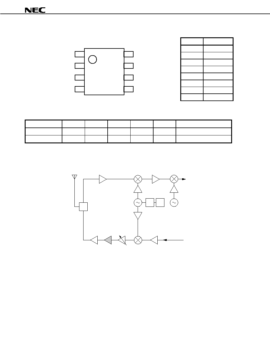
SYSTEM APPLICATION EXAMPLE
SW
N
PLL
RX
TX
PA
driver
PC1678G/GV
µ
˜
Data Sheet P11491EJ4V0DS00
3
µ
µ
µ
µ
PC1678G
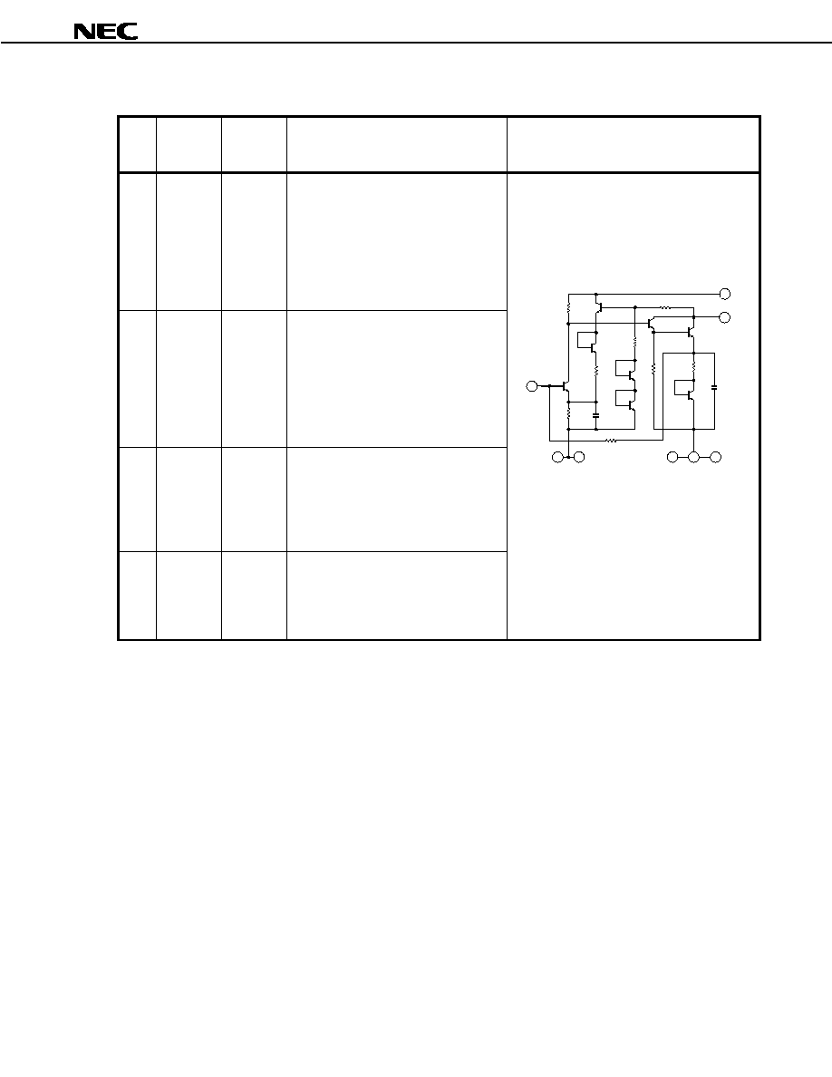
PIN EXPLANATION
Pin
No.
Pin Name
Applied
Voltage
(V)
Function and Applications
Internal Equivalent Circuit
1
INPUT
≠
Signal input pin. A internal matching
circuit, configured with resisters, enables
50
connection over a wide band.
A multi-negative feedback circuit is
designed to cancel the deviations of h
FE
and resistance.
This pin must be coupled to signal source
with capacitor for DC cut.
2
3
4
6
7
GND
0
Ground pin. This pin should be
connected to system ground with
minimum inductance. Ground pattern on
the board should be formed as widely as
possible. All the ground pins must be
connected together with wide ground
pattern to decrease impedance
difference.
5
OUTPUT
Voltage
as same
as V
CC
through
external
inductor
Signal output pin. The inductor must be
attached between V
CC
and output pins to
supply current to the internal output
transistors.
8
V
CC
4.5 to 5.5
Power supply pin, which biases the
internal input transistors.
This pin should be externally equipped
with bypass capacitor to minimize its
impedance.
5
8
1
IN
6
7
2
4
3
V
CC
OUT
GND
GND
2, 3, 4, 6 and 7 are shorted by a lead frame.

Data Sheet P11491EJ4V0DS00
4
µ
µ
µ
µ
PC1678G
ABSOLUTE MAXIMUM RATINGS
Parameter
Symbol
Conditions
Rating
Unit
Supply Voltage
V
CC
T
A
= +25 ∞C, pin 5 and 8
6
V
Power Dissipation
P
D
Mounted on double copper clad 50
◊
50
◊
1.6 mm
epoxy glass PWB (T
A
= +85 ∞C)
360
mW
Operating Ambient Temperature
T
A
-
45 to +85
∞C
Storage Temperature
T
stg
-
55 to +150
∞C
Input Power
P
in
T
A
= +25 ∞C
+10
dBm
RECOMMENDED OPERATING RANGE
Parameter
Symbol
MIN.
TYP.
MAX.
Unit
Notice
Supply Voltage
V
CC
4.5
5.0
5.5
V
The same voltage should be applied
to pin 5 and 8
Operating Ambient Temperature
T
A
-
45
+25
+85
∞C
ELECTRICAL CHARACTERISTICS (T
A
= +25 ∞C, V
CC
= V
out
= 5.0 V, Z
S
= Z
L
= 50
)
Parameter
Symbol
Conditions
MIN.
TYP.
MAX.
Unit
Circuit Current
I
CC
No signal
40.0
49.0
60.0
mA
Power Gain
G
P
f = 500 MHz
21
23
25
dB
Noise Figure
NF
f = 500 MHz
-
6.0
8.0
dB
Upper Limit Operating Frequency
f
u
3 dB down below the gain at 0.1 GHz
1.7
2.0
-
GHz
Isolation
ISL
f = 500 MHz
30
35
-
dB
Input Return Loss
RL
in
f = 500 MHz
11
14
-
dB
Output Return Loss
RL
out
f = 500 MHz
1
4
-
dB
Saturated Output Power
P
O(sat)
f = 500 MHz
+15.5
+17.5
-
dBm

Data Sheet P11491EJ4V0DS00
5
µ
µ
µ
µ
PC1678G
TEST CIRCUIT
1 800 pF
1 800 pF
1 800 pF
V
CC
L
5
1
8
2, 3, 4, 6, 7
OUT
IN
50
50
L: 20.5 T, 2 mm I.D.,
0.25 UEW
(about 300 nH)
INDUCTOR FOR THE OUTPUT PIN
The internal output transistor of this IC consumes 30 mA, to output medium power. To supply current for output
transistor, connect an inductor between the V
CC
pin (pin 8) and output pin (pin 5).
The inductor has both DC and AC effects. In terms of DC, the inductor biases the output transistor with minimum
voltage drop to output enable high level. In terms of AC, the inductor make output-port impedance higher to get
enough gain. In this case, large inductance and Q is suitable.
CAPACITORS FOR THE V
CC
, INPUT AND OUTPUT PINS
Capacitors of 1 800 pF are recommendable as the bypass capacitor for the V
CC
pin and the coupling capacitors
for the input and output pins.
The bypass capacitor connected to the V
CC
pin is used to minimize ground impedance of V
CC
pin. So, stable bias
can be supplied against V
CC
fluctuation.
The coupling capacitors, connected to the input and output pins, are used to cut the DC and minimize RF serial
impedance. Their capacitance are therefore selected as lower impedance against a 50
load. The capacitors thus
perform as high pass filters, suppressing low frequencies to DC.
To obtain a flat gain from 100 MHz upwards, 1 800 pF capacitors are used in the test circuit. In the case of under
100 MHz operation, increase the value of coupling capacitor such as 10 000 pF. Because the coupling capacitors
are determined by equation, C = 1/(2
Rfc).