
Caution Electro-static sensitive devices
The information in this document is subject to change without notice. Before using this document, please
confirm that this is the latest version.
Not all devices/types available in every country. Please check with local NEC representative for
availability and additional information.
BIPOLAR ANALOG INTEGRATED CIRCUIT
µ
µ
µ
µ
PC1686G/GV
GENERAL PURPOSE 5 V FREQUENCY DOWN-CONVERTER IC
Document No. P11100EJ4V0DS00 (4th edition)
Date Published October 1999 N CP(K)
Printed in Japan
DATA SHEET
The mark
shows major revised points.
1996, 1999
©
DESCRIPTION
The
µ
PC1686 is Silicon monolithic IC designed for VHF band receiver applications. This IC consists of double
balanced mixer, local oscillator, IF amplifier, and voltage regulator.
The package is 8-pin SOP or SSOP suitable for high-density surface mount.
FEATURES
∑
VHF/CATV band operation
∑
Single-end push-pull IF amplifier suppresses fluctuation in output impedance.
∑
Good capability of VHF-varactor diode due to balanced amplifier oscillator
∑
Supply voltage: 5 V
∑
Packaged in 8-pin SOP or SSOP suitable for high-density mounting
APPLICATIONS
∑
Tuners for TV and VCR
∑
Receivers for VHF band
ORDERING INFORMATION
Part Number
Package
Supplying Form
µ
PC1686G-E1
8-pin plastic SOP (225 mil)
Embossed tape 12 mm wide.
Pin 1 indicates pull-out direction of tape.
Qty 2.5 kp/reel.
µ
PC1686GV-E1
8-pin plastic SSOP (175 mil)
Embossed tape 8 mm wide.
Pin 1 indicates pull-out direction of tape.
Qty 1 kp/reel.
Remark To order evaluation samples, please contact your local NEC office. (Part number for sample order:
µ
PC1686G,
µ
PC1686GV)
Data Sheet P11100EJ4V0DS00
2
µ
µ
µ
µ
PC1686G/GV
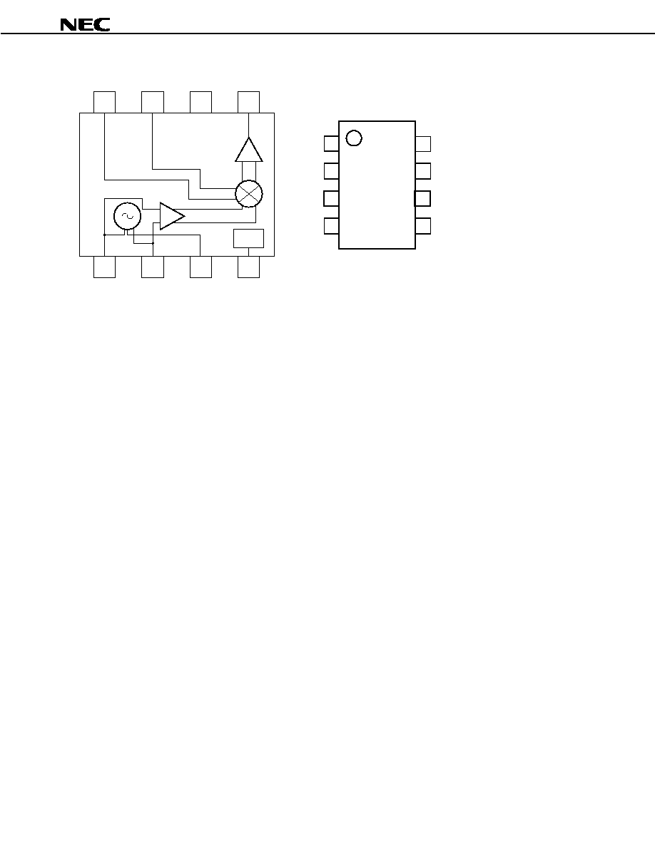
INTERNAL BLOCK DIAGRAM
PIN CONFIGURATION (Top View)
8
7
6
5
1
2
3
4
IF Pre
Amp.
MIX
OSC
OSC
Buffer
REG.
1
2
3
4
8
7
6
5
1.
2.
3.
4.
5.
6.
7.
8.
OSC base (bypass)
OSC base (feedback)
OSC collector (coupling)
V
CC
IF output (open collector)
GND
RF input1 (bypass)
RF input2
Data Sheet P11100EJ4V0DS00
3
µ
µ
µ
µ
PC1686G/GV
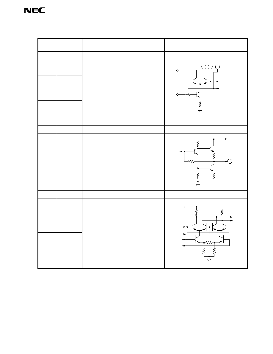
PIN EXPLANATION
Pin
No.
Symbol
Function and Explanation
Equivalent Circuit
1
OSC base
(bypass)
Internal oscillator consists in balance amplifier.
2 pin and 3 pin should be externally equiped
with tank resonater circuit in order to oscillate
with feedback loop.
2
OSC base
(feedback)
1 pin should be grounded through approximate
10 pF coupling capacitor.
3
OSC
collector
(coupling)
V
CC
V
REF
amp.
3
1
2
to OSC buffer
4
V
CC
Supply voltage pin for the IC.
5
IF output
IF output pin. IF amplifier is designed as single-
end push-pull amplifier.
This pin is assigned for the emitter follower
output with 50
constant resistive impedance
in wide band.
V
CC
5
IF
output
from
IF pre
amp.
6
GND
GND pin for the IC.
7
RF input 1
(bypass)
7 pin and 8 pin are inputs for mixer designed as
double balanced type.
Either pin can be assigned for input and another
for ground.
8
RF input 2
V
CC
RF
input
from
OSC
buffer
to IF
amp.
3 pin is defined as open collector. This pin
should be coupled through resistor or
chock coil in order to adjust Q and be
supplied voltage. In case of abnormal
oscillation, adjust its Q lower to stabilize
the operation.
Data Sheet P11100EJ4V0DS00
4
µ
µ
µ
µ
PC1686G/GV
ABSOLUTE MAXIMUM RATINGS
Parameter
Symbol
Conditions
Rating
Unit
Supply Voltage
V
CC
T
A
= +25 ∞C
6.0
V
Power Dissipation
P
D
T
A
= +85 ∞C
Note
250
mW
Operating Ambient Temperature
T
A
-
40 to
+
85
∞C
Storage Temperature
T
stg
-
65 to
+
150
∞C
Note Mounted on 50
◊
50
◊
1.6-mm epoxy glass PWB, with copper patterning on both sides.
RECOMMENDED OPERATING RANGE
Parameter
Symbol
MIN.
TYP.
MAX.
UNIT
Supply Voltage
V
CC
4.5
5.0
5.5
V
Operating Ambient Temperature
T
A
-
40
+
25
+
85
∞C
ELECTRICAL CHARACTERISTICS (V
CC
= 5 V, T
A
= +25
∞
∞
∞
∞
C)
Parameter
Symbol
Conditions
MIN.
TYP.
MAX.
Unit
Circuit Current 1
I
CC
1
no input signal
Note
25
38
48
mA
Conversion Gain 1
CG1
f
RF
= 55 MHz, f
IF
= 44 MHz,
P
RF
=
-
40 dBm, P
OSC
=
-
5 dBm
Note
15
19
22
dB
Conversion Gain 2
CG2
f
RF
= 200 MHz, f
IF
= 50 MHz,
P
RF
=
-
40 dBm, P
OSC
=
-
5 dBm
Note
15.5
19.5
22.5
dB
Conversion Gain 3
CG3
f
RF
= 440 MHz, f
IF
= 50 MHz,
P
RF
=
-
40 dBm, P
OSC
=
-
5 dBm
Note
16
20
23
dB
Noise Figure 1
NF1
f
RF
= 55 MHz, f
IF
= 44 MHz,
P
OSC
=
-
5 dBm
Note
-
11
14
dB
Noise Figure 2
NF2
f
RF
= 200 MHz, f
IF
= 50 MHz
P
OSC
=
-
5 dBm
Note
-
11
14
dB
Noise Figure 3
NF3
f
RF
= 440 MHz, f
IF
= 50 MHz,
P
OSC
=
-
5 dBm
Note
-
12
15
dB
Maximum Output Power 1
P
O(sat)
1
f
RF
= 55 MHz, f
IF
= 44 MHz,
P
RF
= 0 dBm, P
OSC
=
-
5 dBm
Note
-
+
10
-
dBm
Maximum Output Power 2
P
O(sat)
2
f
RF
= 200 MHz, f
IF
= 50 MHz,
P
RF
= 0 dBm, P
OSC
=
-
5 dBm
Note
-
+
10
-
dBm
Maximum Output Power 3
P
O(sat)
3
f
RF
= 440 MHz, f
IF
= 50 MHz,
P
RF
= 0 dBm, P
OSC
=
-
5 dBm
Note
-
+
10
-
dBm
Note By test circuit 1
Data Sheet P11100EJ4V0DS00
5
µ
µ
µ
µ
PC1686G/GV
STANDARD CHARACTERISTICS (FOR REFERENCE) (V
CC
= 5 V, T
A
= +25
∞
∞
∞
∞
C unless otherwise specified)
Parameter
Symbol
Conditions
Reference Values
Unit
Oscillation Frequency Stability
f
stb
V
CC
= ±10 %, f
OSC
= 100 to 490 MHz Note 1
±
100
kHz
Oscillation Frequency Drift
f
drift
f
OSC
= 100 to 490 MHz, 30 min
Note 1
100
kHz
Oscillation Start Voltage
V
OSC
f
OSC
= 100 to 490 MHz
Note 1
3.0
V
1 % Cross-modulation Distortion 1
CM1
f
RF
= 55 MHz, f
IF
= 44 MHz
Note 2, 3
94
dB
µ
1 % Cross-modulation Distortion 2
CM2
f
RF
= 200 MHz, f
IF
= 50 MHz
Note 2, 3
94
dB
µ
1 % Cross-modulation Distortion 3
CM3
f
RF
= 440 MHz, f
IF
= 50 MHz
Note 2, 3
94
dB
µ
Notes 1. By test circuit 2
2. By test circuit 1
3. f
undes
= f
RF
±
12 MHz, P
RF
=
-
31 dBm, P
OSC
=
-
5 dBm
AM: 100 kHz, 30 % Mod., S/I Ratio = 46 dBc, output 75
open