 | –≠–ª–µ–∫—Ç—Ä–æ–Ω–Ω—ã–π –∫–æ–º–ø–æ–Ω–µ–Ω—Ç: UPC1909CX | –°–∫–∞—á–∞—Ç—å:  PDF PDF  ZIP ZIP |

The information in this document is subject to change without notice. Before using this document, please
confirm that this is the latest version.
Not all devices/types available in every country. Please check with local NEC representative for
availability and additional information.
Bipolar Analog Integrated Circuit
µ
µ
µ
µ
PC1909
SWITCHING REGULATOR CONTROL IC
Document No. G14309EJ1V0DS00 (1st edition)
Date Published July 1999 N CP(K)
Printed in Japan
DATA SHEET
1999
©
The
µ
PC1909 is a switching regulator control IC ideal for primary side control of active-clamp type
Note
DC/DC
converters. This IC has 2 outputs employing a totem-pole circuit with peak output current 1.2 A, and is capable of
directly driving a power MOS-FET. As a result, it has been possible to realize primary side control of an active-clamp
type converter on a single chip.
Note It is necessary to obtain license from Vicor Corporation before using the
µ
PC1909 in an active-clamp type
circuit.
FEATURES
∑
2 on-chip outputs; for Q and Q
∑
Capable of directly driving a power MOS-FET
∑
Drive supply voltage range: 7 V to 24 V
∑
On-chip remote control circuit
∑
On-chip pulse-by-pulse overcurrent protection circuit
∑
On-chip overvoltage latch circuit
ORDERING INFORMATION
Part Number
Package
µ
PC1909CX
16-pin plastic DIP (300 mils)
µ
PC1909GS
16-pin plastic SOP (300 mils)
Data Sheet G14309EJ1V0DS00
2
µ
µ
µ
µ
PC1909
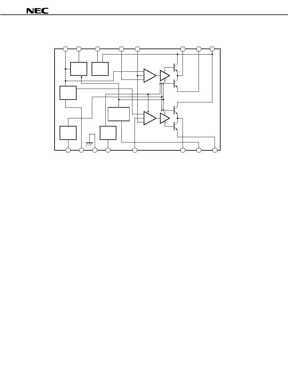
BLOCK DIAGRAM
EMI
1
ON/OFF
OUT
1
V
REF
C
T
R
T
V
CC
DTC
1
FB
OV
C
T2
GND
OC
DTC
2
OUT
2
EMI
2
Over-
current
protection
Over-
voltage
protection
ON/OFF
control
Oscillator
OLS
Reference
power
supply
PWM
comparator 1
≠
+
+
PWM
comparator 2
+
≠
≠
1
2
3
4
5
6
7
8
16
15
14
13
12
11
10
9

Data Sheet G14309EJ1V0DS00
3
µ
µ
µ
µ
PC1909
PIN CONFIGURATION (TOP VIEW)
16-pin plastic DIP (300 mils)
µ
µ
µ
µ
PC1909CX
16-pin plastic SOP (300 mils)
µ
µ
µ
µ
PC1909GS
1
2
3
4
16
15
14
13
5
12
6
11
7
10
8
9
C
T
R
T
V
REF
DTC
1
EMI
1
V
CC
OUT
1
FB
OV
C
T2
GND
OC
DTC
2
OUT
2
ON/OFF
EMI
2
PIN FUNCTION LIST
Pin Number
Pin Name
Function
Pin Number
Pin Name
Function
1
OV
Overvoltage protection
9
V
CC
Power supply
2
C
T2
OLS shift setting
10
EMI
1
OUT
1
emitter
3
GND
Ground
11
OUT
1
OUT
1
output
4
OC
Overcurrent protection
12
FB
Feedback input
5
DTC
2
OUT
2
dead-time setting
13
DTC
1
OUT
1
dead-time setting
6
OUT
2
OUT
2
output
14
V
REF
Reference voltage output
7
ON/OFF
ON/OFF control
15
R
T
Timing resistance
8
EMI
2
OUT
2
emitter
16
C
T
Timing capacitance

Data Sheet G14309EJ1V0DS00
4
µ
µ
µ
µ
PC1909
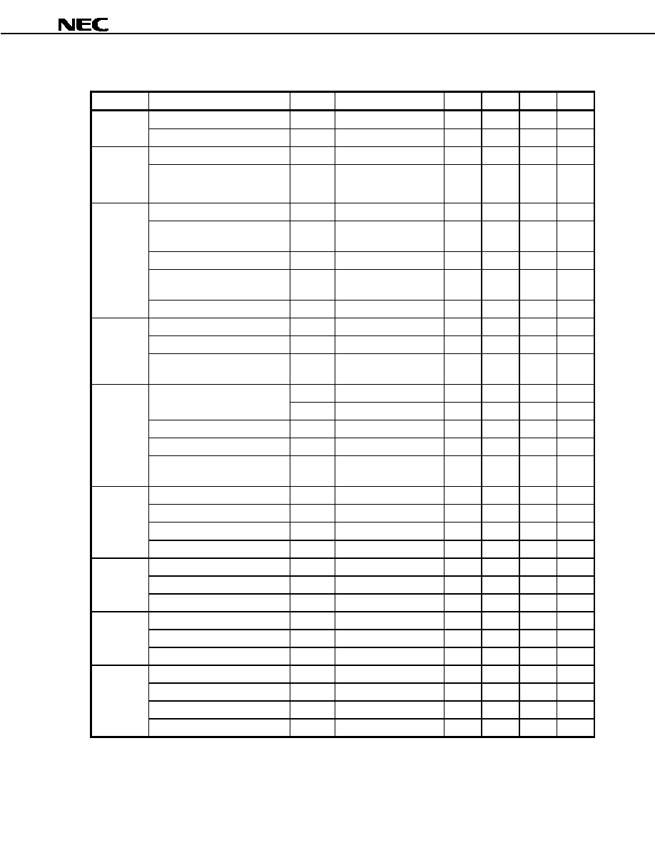
ELECTRICAL SPECIFICATIONS
Absolute Maximum Ratings (Unless otherwise specified, T
A
= 25
∞
∞
∞
∞
C)
Parameter
Symbol
µ
PC1909CX
µ
PC1909GS
Unit
Supply Voltage
V
CC
26
V
Output Current (DC, per output)
I
C (DC)
100
mA
Output Current (peak, per output)
I
C (peak)
1.2
A
Total Power Dissipation
P
T
1000
694
mW
Operating Ambient Temperature
T
A
-
20 to +85
∞
C
Operating Junction Temperature
T
J
-
20 to +150
∞
C
Storage Temperature
T
stg
-
55 to +150
∞
C
Caution Product quality may suffer if the absolute maximum rating is exceeded even momentarily for any
parameter. That is, the absolute maximum ratings are rated values at which the product is on
the verge of suffering physical damage, and therefore the product must be used under
conditions that ensure that the absolute maximum ratings are not exceeded.
Recommended Operating Conditions
Parameter
Symbol
MIN.
TYP.
MAX.
Unit
Supply Voltage
V
CC
7
10
24
V
Oscillation Frequency
f
OSC
50
200
500
kHz
Output Load Capacitance
C
L
2200
3000
pF
Output Load Resistance
R
L
10
k
Operating Junction Temperature
T
J
-
20
+100
∞
C
Data Sheet G14309EJ1V0DS00
5
µ
µ
µ
µ
PC1909
Electrical Characteristics (Unless otherwise specified, T
A
= 25
∞
∞
∞
∞
C, V
CC
= 10 V, R
T
= 10 k
, fosc = 200 kHz)
Block
Parameter
Symbol
Conditions
MIN.
TYP.
MAX.
Unit
Standby Current
I
CC (SB)
V
CC
= 7 V
0.1
mA
Total
Circuit Current
I
CC
Without load
6
12
18
mA
Start-Up Threshold Voltage
V
CC (L to H)
8
9
10
V
Under-
Voltage
Lockout
Circuit
Operating Voltage Hysteresis
Width
V
H
3
4
5
V
Output Voltage
V
REF
I
REF
= 0 A
4.7
4.9
5.1
V
Line Regulation
REG
IN
8 V
V
CC
15 V,
I
REF
= 0 A
1
10
mV
Load Regulation
REG
L
1 mA
I
REF
4 mA
6
12
mV
Output Voltage Temperature
Coefficient
V
REF
/
T
-
10
∞
C
T
A
+85
∞
C,
I
REF
= 0 A
400
(700)
µ
V/
∞
C
Reference
Voltage
Short Circuit Current
I
O short
I
REF
= 0 A
15
mA
Oscillation Frequency
f
OSC
180
200
220
kHz
Frequency Line Regulation
f/
V
8 V
V
CC
15 V
1
%
Oscillation
Frequency Temperature
Coefficient
f/
T
-
10
∞
C
T
A
+85
∞
C
2
(5)
%
I
B (COMP1)
V
COMP1
= V
REF
10
µ
A
Input Bias Current
I
B (COMP2)
V
COMP2
= V
REF
10
µ
A
Low-level Threshold Voltage
V
TH (L)
1.5
V
High-level Threshold Voltage
V
TH (H)
3.5
V
PWM
Comparator
Dead-time Temperature
Coeficient
DT/
T
-
10
∞
C
T
A
+85
∞
C,
V
D
= 0.46 V
REF
3
%
Low-level Output Voltage
V
OL
I
SINK
= 3 mA
0.5
V
High-level Output Voltage
V
OH
I
SOURCE
= 30 mA
V
CC
-
1.6
V
Rise Time
t
r
R
L
= 15
, C
L
= 2200 pF
60
ns
Output
Fall Time
t
f
R
L
= 15
, C
L
= 2200 pF
40
ns
Input Voltage at Output ON
V
IN (ON)
2.4
2.6
2.8
V
Input Voltage at Output OFF
V
IN (OFF)
2.2
2.4
2.6
V
Remote
Control
Hysteresis Width
V
H
0.1
0.2
0.3
V
Overcurrent Threshold Voltage
V
TH (OC)
190
210
230
mV
Input Bias Current
I
B (OC)
V
CC
= 0 V
200
µ
A
Overcurrent
Latch
Delay to Output
t
d (OC)
150
ns
Overvoltage Threshold Voltage
V
TH (OV)
2
2.4
2.8
V
Input Bias Current
I
B (OV)
V
OV
= V
REF
4
µ
A
OVL Reset Voltage
V
R (OV)
2
V
Overvoltage
Latch
Delay to Output
t
d (OV)
750
ns
Remark Values in parentheses ( ) represent reference values.