 | –≠–ª–µ–∫—Ç—Ä–æ–Ω–Ω—ã–π –∫–æ–º–ø–æ–Ω–µ–Ω—Ç: UPC1934 | –°–∫–∞—á–∞—Ç—å:  PDF PDF  ZIP ZIP |
Document Outline
- COVER
- DESCRIPTION
- FEATURES
- ORDERING INFORMATION
- BLOCK DIAGRAM
- PIN CONFIGURATION (Top view)
- PIN FUNCTIONS
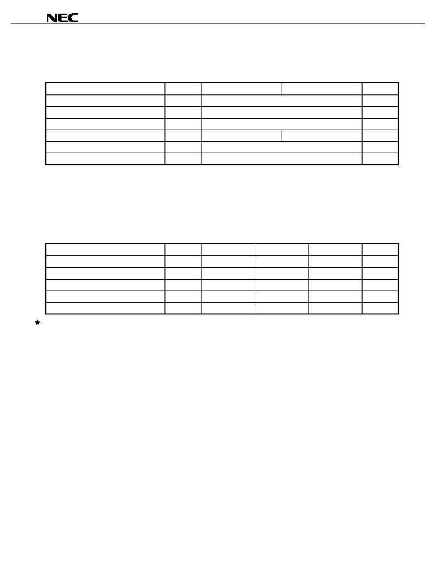
- 1. ELECTRICAL SPECIFICATIONS
- 2. CONFIGURATION AND OPERATION OF EACH BLOCK
- 2.1 Reference Voltage Generator
- 2.2 Oscillator
- 2.3 Under Voltage Lock-out Circuit
- 2.4 Error Amplifiers
- 2.5 PWM Comparators
- 2.6 Timer Latch-Method Short Circuit Protection Circuit
- 2.7 Output Circuit
- 3. NOTES ON USE
- 3.1 Setting the Output Voltage
- 3.2 Setting the Oscillation Frequency
- 3.3 Preventing Malfunction of the Timer Latch-Method Short Circuit Protection Circuit
- 3.4 Connecting Unused Error Amplifiers
- 3.5 ON/OFF Control
- 3.6 Notes on Actual Pattern Wiring
- 4. APPLICATION EXAMPLE
- 4.1 Application Example
- 4.2 List of External Parts
- 5. PACKAGE DRAWINGS
- 6. RECOMMENDED SOLDERING CONDITIONS

The information in this document is subject to change without notice. Before using this document, please
confirm that this is the latest version.
Not all devices/types available in every country. Please check with local NEC representative for
availability and additional information.
1998
BiCMOS INTEGRATED CIRCUIT
µ
µ
µ
µ
PC1934
DC-DC CONVERTER CONTROL IC
DATA SHEET
Document No. G13567EJ3V0DS00 (3rd edition)
Date Published April 2000 NS CP (K)
Printed in Japan
The mark
5
shows major revised points.
DESCRIPTION
The
µ
PC1934 is an IC that controls a low-voltage input DC-DC converter. This IC is suitable for an operation with 3-V,
3.3-V input or a lithium ion secondary battery input, because the minimum operation supply voltage is 2.5 V. Because of
its wide operating voltage range, it can also be used to control DC-DC converters that use an AC adapter for input.
FEATURES
∑
Low supply voltage: 2.5 V (MIN.)
∑
Operating voltage range: 2.5 to 20 V (breakdown voltage: 30 V)
∑
Timer latch circuit for short-circuit protection.
∑
Ceramic capacitor with low capacitance (0.1
µ
F) can be used for short-circuit protection.
∑
Open drain outputs (Each of the outputs can be used to control a step-down converter, a step-up converter and an
inverted converter.)
∑
Can control two output channels.
ORDERING INFORMATION
Part Number
Package
µ
PC1934GR-1JG
16-pin plastic SSOP (5.72 mm (225))
µ
PC1934GR-PJG
16-pin plastic TSSOP (5.72 mm (225))

Data Sheet G13567EJ3V0DS00
2
µ
µ
µ
µ
PC1934
BLOCK DIAGRAM
DLY
I
N2
V
REF
E/A
2
E/A
1
PWM
1
PWM
2
I
I2
OUT
2
V
CC
DTC
2
FB
2
+
≠
≠
Timer latch for
short-circuit
protection section
Reference
voltage
section
Oscillation
section
GND
OUT
1
FB
1
R
T
C
T
I
I1
I
N1
DTC
1
≠
+
≠
MOS input
MOS output
MOS input
MOS output
Channel 1
Channel 2
+
≠
≠
+
1
2
3
4
5
6
7
8
16
15
14
13
12
11
10
9

Data Sheet G13567EJ3V0DS00
3
µ
µ
µ
µ
PC1934
PIN CONFIGURATION (Top View)
16-pin plastic SSOP (5.72 mm (225))
∑
∑
∑
∑ µµµµ
PC1934GR-1JG
16-pin plastic TSSOP (5.72 mm (225))
∑
∑
∑
∑ µµµµ
PC1934GR-PJG
PIN FUNCTIONS
Pin No.
Symbol
Function
Pin No.
Symbol
Function
1
C
T
Frequency setting capacitor connection
9
V
CC
Power supply
2
R
T
Frequency setting resistor connection
10
OUT
2
Channel 2 open drain output
3
I
N1
Channel 1 error amplifier non-inverted
input
11
DTC
2
Channel 2 dead time setting
4
I
I1
Channel 1 error amplifier inverted input
12
FB
2
Channel 2 error amplifier output
5
FB
1
Channel 1 error amplifier output
13
I
I2
Channel 2 error amplifier inverted input
6
DTC
1
Channel 1 dead time setting
14
I
N2
Channel 2 error amplifier non-inverted
input
7
OUT
1
Channel 1 open drain output
15
DLY
Delay capacitor connection of short-
circuit protection
8
GND
Ground
16
V
REF
Reference voltage output
1
2
3
4
16
15
14
13
5
12
6
11
7
10
8
9
V
REF
DLY
I
N2
I
I2
OUT
2
V
CC
DTC
2
FB
2
C
T
R
T
I
N1
I
I1
FB
1
DTC
1
OUT
1
GND

Data Sheet G13567EJ3V0DS00
4
µ
µ
µ
µ
PC1934
CONTENTS
1.
ELECTRICAL SPECIFICATIONS ................................................................................................................ 5
2.
CONFIGURATION AND OPERATION OF EACH BLOCK.................................................................... 10
2.1
Reference Voltage Generator ...........................................................................................................................10
2.2
Oscillator ...........................................................................................................................................................10
2.3
Under Voltage Lock-out Circuit ........................................................................................................................11
2.4
Error Amplifiers.................................................................................................................................................11
2.5
PWM Comparators ............................................................................................................................................11
2.6
Timer Latch-Method Short Circuit Protection Circuit ....................................................................................11
2.7
Output Circuit ....................................................................................................................................................11
3.
NOTES ON USE........................................................................................................................................ 12
3.1
Setting the Output Voltage ...............................................................................................................................12
3.2
Setting the Oscillation Frequency ...................................................................................................................13
3.3
Preventing Malfunction of the Timer Latch-Method Short Circuit Protection Circuit..................................13
3.4
Connecting Unused Error Amplifiers ..............................................................................................................13
3.5
ON/OFF Control.................................................................................................................................................14
3.6
Notes on Actual Pattern Wiring........................................................................................................................14
4.
APPLICATION EXAMPLE ......................................................................................................................... 15
4.1
Application Example.........................................................................................................................................15
4.2
List of External Parts ........................................................................................................................................15
5.
PACKAGE DRAWINGS.............................................................................................................................. 16
6.
RECOMMENDED SOLDERING CONDITIONS ....................................................................................... 18
Data Sheet G13567EJ3V0DS00
5
µ
µ
µ
µ
PC1934
1.
ELECTRICAL SPECIFICATIONS
Absolute Maximum Ratings (unless otherwise specified, T
A
=
=
=
=
25
∞
∞
∞
∞
C)
Parameter
Symbol
µ
PC1934GR-1JG
µ
PC1934GR-PJG
Unit
Supply voltage
V
CC
30
V
Output voltage
V
O
30
V
Output current (open drain output)
I
O
21
mA
Total power dissipation
P
T
417
400
mW
Operating ambient temperature
T
A
≠20 to + 85
∞
C
Storage temperature
T
stg
≠55 to + 150
∞
C
Caution
Product quality may suffer if the absolute maximum rating is exceeded even momentarily for any
parameter. That is, the absolute maximum ratings are rated values at which the product is on the verge
of suffering physical damage, and therefore the product must be used under conditions that ensure
that the absolute maximum ratings are not exceeded.
Recommended Operating Conditions
Parameter
Symbol
MIN.
TYP.
MAX.
Unit
Supply voltage
V
CC
2.5
20
V
Output voltage
V
O
0
20
V
Output current
I
O
20
mA
Operating temperature
T
A
-
20
+
85
∞
C
Oscillation frequency
f
OSC
20
1000
kHz
Caution
The recommended operating range may be exceeded without causing any problems provided that the
absolute maximum ratings are not exceeded. However, if the device is operated in a way that exceeds
the recommended operating conditions, the margin between the actual conditions of use and the
absolute maximum ratings is small, and therefore thorough evaluation is necessary. The recommended
operating conditions do not imply that the device can be used with all values at their maximum values.
Data Sheet G13567EJ3V0DS00
6
µ
µ
µ
µ
PC1934
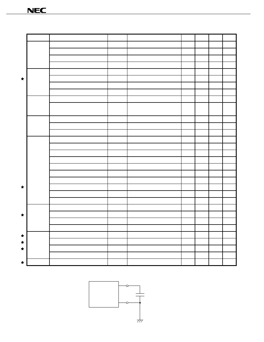
Electrical Characteristics (unless otherwise specified, T
A
=
25
∞
∞
∞
∞
C, V
CC
=
=
=
=
3 V, f
OSC
= 100 kHz)
Block
Parameter
Symbol
Conditions
MIN.
TYP.
MAX.
Unit
Start-up voltage
V
CC (L-H)
I
REF
= 0.1 mA
1.57
V
Operation stop voltage
V
CC (H-L)
I
REF
= 0.1 mA
1.5
V
Hysteresis voltage
V
H
I
REF
= 0.1 mA
30
70
mV
Under
voltage
Lock-out
section
Reset voltage (timer latch)
V
CCR
I
REF
= 0.1 mA
1.0
V
Reference voltage
V
REF
I
REF
= 1 mA
2.0
2.1
2.2
V
Line regulation
REG
IN
2.5 V
V
CC
20 V
2
12.5
mV
Load regulation
REG
L
0.1 mA
I
REF
1 mA
2
7.5
mV
Reference
Voltage
section
Temperature coefficient
V
REF
/
T
-
20
∞
C
T
A
+
85
∞
C, I
REF
= 0 A
0.5
%
f
OSC
setting accuracy
f
OSC
R
T
= 11 k
, C
T
= 330 pF
-
15
+
15
%
Oscillation
section
f
OSC
total stability
f
OSC
-
20
∞
C
T
A
+
85
∞
C,
2.5 V
V
CC
20 V
-
30
+
30
%
Input bias current
I
BD
0.4
1.0
µ
A
Low-level threshold voltage
V
TH (L)
Duty = 100 %
1.2
V
Dead time
control
section
High-level threshold voltage
V
TH (H)
Duty = 0 %
1.6
V
Input offset voltage
V
IO
-
10
+
10
mV
Input offset current
I
IO
-
100
+
100
nA
Input bias current
I
B
-
100
+
100
nA
Common mode input voltage range
V
IMC
0
0.4
V
Open loop gain
A
v
V
O
= 0.3 V
70
80
dB
Unity gain
f
unity
V
O
= 0.3 V
1.5
MHz
Maximum output voltage (
+
)
V
OM
+
I
O
=
-
45
µ
A
1.6
2
V
Maximum output voltage (
-
)
V
OM
-
I
O
= 45
µ
A
0.02
0.5
V
Output sink current
I
Osink
V
FB
= 0.5 V
0.8
1.4
mA
Error
Amplifier
section
Output source current
I
Osource
V
FB
= 1.6 V
-
70
-
45
µ
A
Drain cutoff current
I
LEAK
V
O
= 30 V
100
µ
A
Output ON voltage
V
OL
R
L
= 150
0.2
0.6
V
Rise time
t
r
R
L
= 150
50
ns
Output
section
Fall time
t
f
R
L
= 150
60
ns
Input sense voltage
V
TH
0.5
0.63
0.75
V
UV sense voltage
V
UV
0.6
0.8
0.95
V
Source current on short-circuiting
I
OUV
1.0
1.6
2.5
µ
A
Short-circuit
Protection
section
Delay time
t
DLY
C
DLY
= 0.1
µ
F
50
ms
Overall
Circuit operation current
I
CC
V
CC
= 3 V
1.4
2.2
3.7
mA
Caution Connect a capacitor of 0.01 to 10
µ
µ
µ
µ
F to the V
REF
pin.
C
REF
= 0.01 to 10 F
µ
µ
PC1934
16
8

Data S
h
e
e
t
G1
356
7E
J3V
0
DS
0
0
7
µ
µ
µ
µ
PC1934
Channel 1
Channel 1 soft start
Normal operation
OUT
1
Short-load
Stop output
OFF
ON
DTC
1
FB
1
C
T
V
TH
Channel 2
OUT
2
DLY
OFF
ON
DTC
2
FB
2
C
T
V
UV
Remark These timings are an example when the channel 1 output has been a short- load. The outputs of channel 1 and 2 are also stopped when a short-
circuit protection circuit starts operation by detecting a short- load of channel 2.
Timing Charts

Data Sheet G13567EJ3V0DS00
8
µ
µ
µ
µ
PC1934
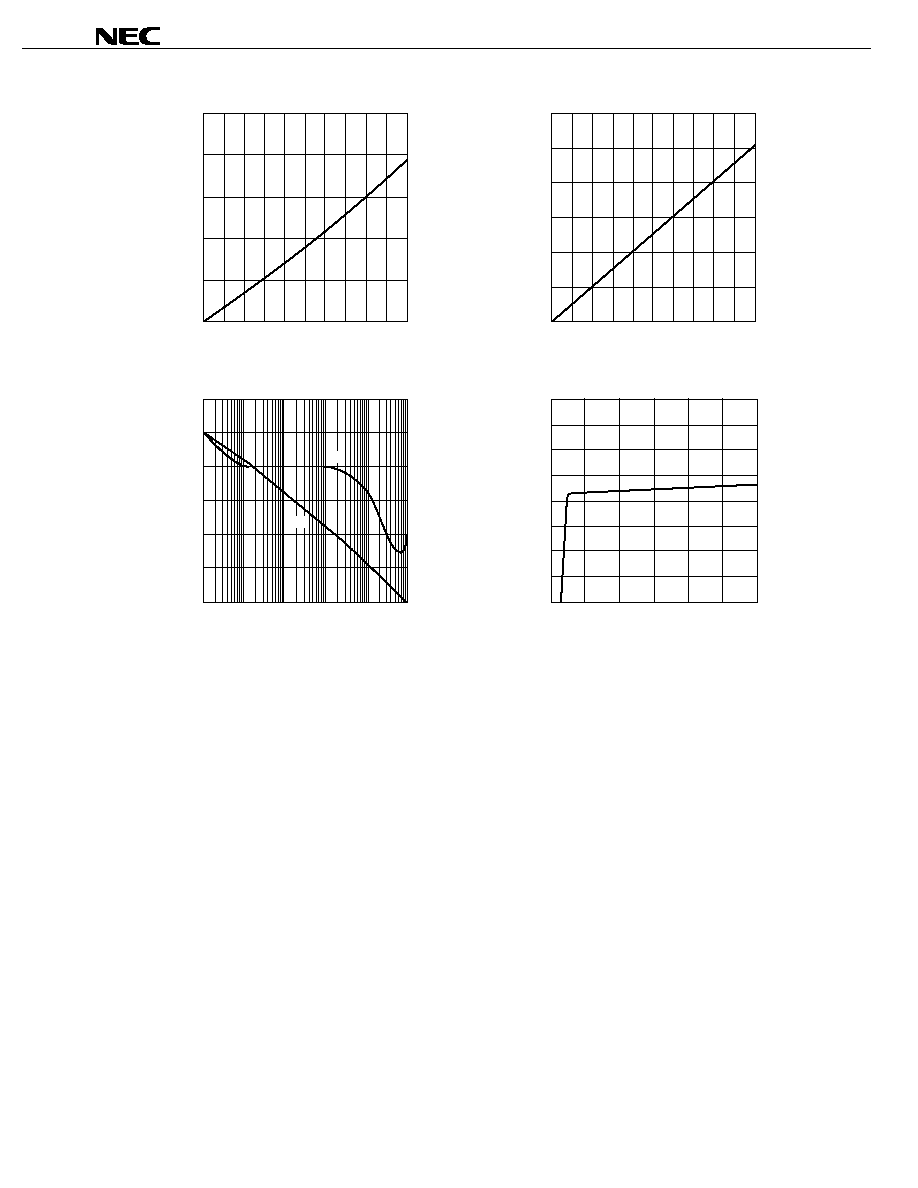
Typical Characteristic Curves (unless otherwise specified, V
CC
= 3 V, f
OSC
= 100 kHz, T
A
= 25
∞
∞
∞
∞
C) (Nominal)
V
REF
vs V
CC
2.5
2.0
1.5
1.0
0.5
0
1
2
3
4
5
Supply voltage V
CC
(V)
Reference voltage V
REF
(V)
I
REF
= 0 A
P
T
vs T
A
0.5
0.4
0.3
0.2
0.1
0
25
50
75
100
125
150
Operating ambient temperature T
A
(
∞
C)
Total power dissipation P
T
(W)
300
∞
C/W
PC1934GR-1JG
µ
312.5
∞
C/W
PC1934GR-PJG
µ
V
REF
vs T
A
2.13
2.12
2.11
2.10
2.08
2.07
2.09
≠25
0
25
50
75
100
I
REF
= 0 A
Operating ambient temperature T
A
(
∞
C)
Reference voltage V
REF
(V)
f
OSC
vs R
T
1000
100
10
1
10
1000
100
Timing resistance R
T
(k
)
Oscillation frequency f
OSC
(kHz)
C
T
= 150 pF
C
T
= 1500 pF
C
T
= 330 pF
f
OSC
vs T
A
6
4
2
0
≠2
≠4
≠6
0
≠25
25
50
75
100
R
T
= 10 k
C
T
= 330 pF
Operating ambient temperature T
A
(
∞
C)
Oscillation frequency accuracy
f
OSC
(%)
V
OL
vs T
A
0.5
0.4
0.3
0.2
0.1
0
0
≠25
25
75
50
100
Output ON voltage V
OL
(V)
Operating ambient temperature T
A
(
∞
C)
I
O
= 20 mA
Data Sheet G13567EJ3V0DS00
9
µ
µ
µ
µ
PC1934
V
OL
vs I
O
0.5
0.4
0.3
0
0.1
0.2
4
8
12
16
20
Output current I
O
(mA)
Output ON voltage V
OL
(V)
t
DLY
vs C
DLY
600
500
400
300
200
100
0
1.0
0.8
0.6
0.4
0.2
DLY pin capacitor capacitance C
DLY
( F)
Short-circuit protection circuit delay time t
DLY
(ms)
µ
100
60
80
40
20
0
≠20
100
10 k
1 k
10 M
≠90
≠20
0
45
90
135
180
1 M
100 k
Frequency f (Hz)
Gain A
v
(dB)
A
v
, vs f
A
v
Phase (deg)
I
CC
vs V
CC
4
3
2
1
0
5
10
15
20
25
30
Supply voltage V
CC
(V)
Circuit operation I
CC
(mA)

Data Sheet G13567EJ3V0DS00
10
µ
µ
µ
µ
PC1934
2.
CONFIGURATION AND OPERATION OF EACH BLOCK
Figure 2-1 Block Diagram
2.1
Reference Voltage Generator
The reference voltage generator is comprised of a band-gap reference circuit, and outputs a temperature-compensated
reference voltage (2.1 V). The reference voltage can be used as the power supply for internal circuits, or as a reference
voltage, and can also be accessed externally via the V
REF
pin (pin 16).
2.2
Oscillator
The oscillator self-oscillates if a timing resistor is attached to the R
T
pin (pin 2). Also, the oscillator outputs the
symmetrical triangular waveform if a timing capacitor is attached to the C
T
pin (pin 1). This oscillator waveform is input to
the non-inverted input pins of the two PWM comparators to determine the oscillation frequency.
8
10
Error amplifier
Output
section
PWM
comparator
SCP
comparator
OUT
2
DTC
2
FB
2
I
I2
7
Error amplifier
Output
section
PWM
comparator
OUT
1
DTC
1
FB
1
I
I1
1
C
T
2
R
T
Oscillation
section
S
Q
Q
GND
DLY
C
DLY
15
0.63 V
9
V
CC
11
12
13
6
5
4
16
V
REF
Q
2
Q
1
Reference
voltage
section
Under voltage
lock-out
section
I
N1
3
I
N2
14
Timer latch for
short-circuit
protection section

Data Sheet G13567EJ3V0DS00
11
µ
µ
µ
µ
PC1934
2.3
Under Voltage Lock-out Circuit
The under voltage lock-out circuit prevents malfunctioning of the internal circuits when the supply voltage is low, such as
when the supply voltage is first applied, or when the power supply is interrupted. When the voltage is low, the two output
transistors are cut off at the same time.
2.4
Error Amplifiers
The circuits of the error amplifiers E/A
1
and E/A
2
are exactly the same. The first stage of the error amplifier is a P-
channel MOS transistor input. Be careful of the input voltage ranges (the common mode input voltage ranges are all 0 to
0.4 V (TYP.)).
2.5
PWM Comparators
The output ON duty is controlled according to the outputs of the error amplifiers and the voltage input to the Dead Time
Control pin.
A triangular waveform is input to the non-inverted pin, and the error amplifier output and Dead Time Control pin voltage
are input to the inverted pins of the PWM comparators. Therefore, the output transistor ON period is the period when the
triangular waveform is higher than the error amplifier output and Dead Time Control pin voltage (refer to Timing Charts).
2.6
Timer Latch-Method Short Circuit Protection Circuit
When the converter outputs either a channel or both channels drop, the FB outputs of the error amplifiers of those
outputs go low. If the FB output goes lower than the timer latch input detection voltage (V
TH
= 0.63 V)), then the output of
the SCP comparator goes low, and Q
1
goes off.
When Q
1
turns OFF, the constant-current supply charges C
DLY
via the DLY pin. The DLY pin is internally connected to a
flip-flop. When the DLY pin voltage reaches the UV detection voltage (V
UV
= 0.8 V (TYP.)), the output Q of the flip-flop goes
low, and the output stage of each channel is latched to OFF (refer to Figure 2-1 Block Diagram).
Make the power supply voltage briefly less than the reset voltage (V
CCR
, 1.0 V TYP.) to reset the latch circuit when the
short-circuit protection circuit has operated.
2.7
Output Circuit
The output circuit has an N-channel open-drain output providing an output withstand voltage of 30 V (absolute maximum
rating), and an output current of 21 mA (absolute maximum rating).
Data Sheet G13567EJ3V0DS00
12
µ
µ
µ
µ
PC1934
3.
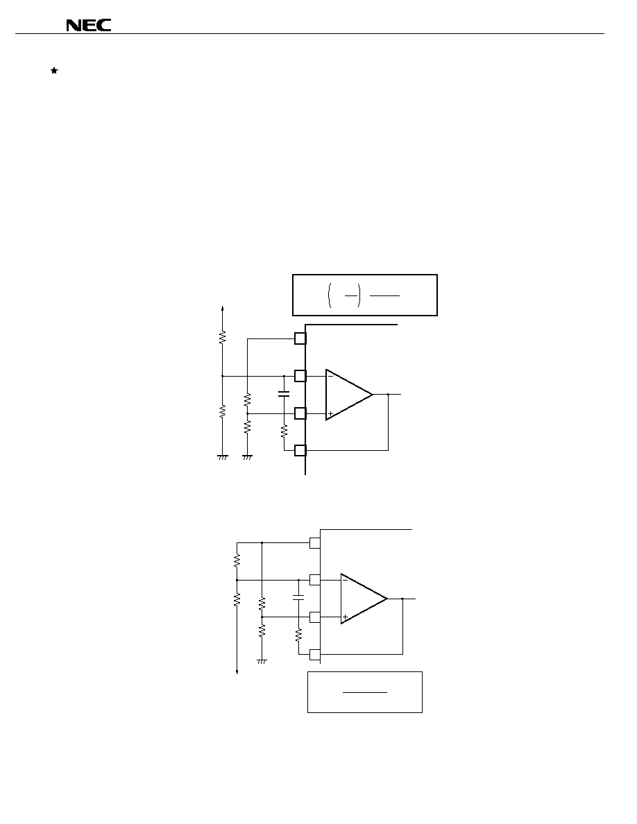
NOTES ON USE
3.1
Setting the Output Voltage
Figure 3-1 illustrates the method of setting the output voltage. The output voltage is obtained using the formula shown in
the figure.
The common mode input voltage range of the error amplifier is 0 to 0.4 V (TYP.) for both the error amplifiers, E/A
1
and
E/A
2
. Therefore, select a resistor value that gives this voltage range.
Figure 3-1 Setting the Output Voltage
(1) When setting a positive output voltage using error amplifier E/A
1
.
(2) When setting a negative output voltage using error amplifier E/A
2
.
16
4
3
5
R
NF
C
NF
R
4
R
3
R
2
R
1
V
REF
V
REF
V
OUT
(positive voltage)
V
OUT
= 1 +
R
1
R
2
∑
∑
R
4
R
3
+ R
4
E/A
1
16
13
14
12
R
NF
C
NF
R
4
R
3
R
2
R
1
V
REF
V
REF
V
OUT
(negative voltage)
V
OUT
=
∑
R
1
R
4
-
R
2
R
3
R
1
(R
3
+R
4
)
E/A
2

Data Sheet G13567EJ3V0DS00
13
µ
µ
µ
µ
PC1934
3.2
Setting the Oscillation Frequency
Choose R
T
according to the oscillation frequency (f
OSC
) vs timing resistor (C
T
, R
T
) characteristics (refer To Typical
Characteristics Curves f
OSC
vs C
T
, R
T
). The formula below (3-1) gives an approximation of f
OSC
. However, the result of
formula 3-1 is only an approximation, and the value must be confirmed in actual operation, especially for high-frequency
operation.
f
OSC
[Hz]
0.375/(C
T
[F] x R
T
[
]) (3-1)
3.3
Preventing Malfunction of the Timer Latch-Method Short Circuit Protection Circuit
The timer latch short-circuit protection circuit operates when the error amplifier outputs (pin 5 and 12) goes below
approximately 0.63 V, and cuts off the output. However, if the rise of the power supply voltage is fast, or if there is noise on
the DLY pin (pin 15), the latch circuit may malfunction and cut the output off.
To prevent this, lower the wiring impedance between the DLY pin and the GND pin (pin 8), and avoid applying noise to
the DLY pin.
3.4
Connecting Unused Error Amplifiers
When one of the two control circuits is used, connect the circuit so that the output of the error amplifier of unused circuit
is high. Figure 3-2 shows examples of how to connect unused error amplifiers.
Figure 3-2 Examples of Connecting Unused Error Amplifiers
(1) Error amplifier E/A
1
(2) Error amplifier E/A
2
16
3
4
5
6
V
REF
DTC
1
E/A
1
16
14
13
12
11
V
REF
DTC
2
E/A
2

Data Sheet G13567EJ3V0DS00
14
µ
µ
µ
µ
PC1934
3.5
ON/OFF Control
The ON/OFF control method of the output oscillation is to input the ON/OFF signal from ON as shown in Figure 3-3.
The PWM converter can be turned ON/OFF by controlling the level of the DTC pin. However, it is necessary to keep the
level of the FB
output high so that the timer latch does not start when the PWM converter is OFF. In this circuit example,
the FB
output level is controlled by controlling the level of the I
I
pin.
Figure 3-3 ON/OFF Control
(1) When ON is high: OFF status
Q
1
: ON
Q
2
: ON
DTC pin: High level
Output duty of PWM comparator: 0 %
Q
3
: ON
I
I
pin: Low level
FB output: High level
SCP comparator output: High level
Q is ON.
Timer latch stops.
(2) When ON
3
is low: ON status
Q
1
: OFF
Q
2
is OFF.
C
1
is charged in the sequence of [V
REF
C
1
R
4
]
DTC pin voltage drops.
Soft start
Q
3
: OFF
I
I
pin: High level
FB output: Low level
SCP comparator output: Low level
Q: OFF
Charging C
DLY
starts (timer latch start).
Caution Keep the high-level voltage of the DTC pin at 1.6 V or higher and the low-level voltage of the I
I
pin
within (R6/(R5+R6))
∑
∑
∑
∑
V
REF
. The maximum voltage that is applied to the I
I
pin must be equal to or lower
than V
REF
.
3.6
Notes on Actual Pattern Wiring
When actually carrying out the pattern wiring, it is necessary to separate control-related grounds and power-related
grounds, and make sure that they do not share impedances as far as possible. In addition, make sure the high-frequency
impedance is lowered using capacitors and other components to prevent noise input to the V
REF
pin.
≠
≠
+
+
≠
≠
+
ON
Q
1
Q
2
Q
3
Q
PWM
comparator
DTC
R
2
V
REF
C
DLY
C
1
FB
DLY
R
1
V
O
R
5
R
6
V
REF
R
4
R
3
I
I
I
N
0.3 V
0.63 V
Error
amplifier
To output stage
Oscillation section
(common to each channel)
SCP comparator
(common to each channel)

Data Sheet G13567EJ3V0DS00
15
µ
µ
µ
µ
PC1934
4.
APPLICATION EXAMPLE
4.1
Application Example
Figure 4-1 shows an example circuit for obtaining
±
5 V/50 mA from a +3 V power supply.
Figure 4-1 Chopper-Method Step-up/Inverting-Type Switching Regulator
4.2
List of External Parts
The list below shows the external parts.
Table 4-1 List of External Parts
Symbol
Parameter
Function
Part number
Maker
Remark
C
2
10
µ
F
Input stable capacitor
25SC10M
SANYO
OS-CON, SC series
C
14
68
µ
F
Output capacitor
20SA68M
SANYO
OS-CON, SA series
D
11
Schottkey diode
D1FS4
SHINDENGEN
L
11
100
µ
H
Choke inductor
636FY-101M
TOKO
D73F series
Q
11
, Q
12
Buffer transistor
µ
PA609T
NEC
Transistor array
Q
13
Switching transistor
2SB1572
NEC
C
21
68
µ
F
Output capacitor
20SA68M
SANYO
OS-CON, SA series
D
21
Schottkey diode
D1FS4
SHINDENGEN
L
21
100
µ
H
Choke inductor
636FY-101M
TOKO
D73F series
Q
21
, Q
22
Buffer transistor
µ
PA609T
NEC
Transistor array
Q
23
Switching transistor
2SD2403
NEC
Remarks 1.
The capacitors that are not specified in the above list are multilayer ceramic capacitors.
2.
The resistors that are not specified in the above list are 1/4W resistors.
4
1
2
3
8
5
6
7
13
16
15
14
9
12
11
10
µ
F
CH2
V
O
= +5.0 V
I
O
= 50 mA
CH1
V
O
=
-
5.0 V
I
O
= 50 mA
GND
GND
R
21
47 k
C
24
68
µ
H
µ
F
C
14
68
R
22
5 k
R
214
10 k
R
12
20 k
R
11
5.1 k
R
111
470
R
111
10
R
212
10
R
210
470
R
211
24 k
R
24
2 k
R
23
12 k
R
18
12 k
R
18
2 k
R
18
12 k
R
16
10 k
R
17
5 k
R
19
80
R
29
510
R
T
R
111
100
C
23
100 pF
C
T
100 pF
C
11
1
C
11
C
23
3300 pF
C
23
3300 pF
5.1 k
R
25
12 k
R
15
12 k
R
26
10 k
R
27
5 k
R
28
15 k
C
2
10
C
1
1
R
113
10 k
R
112
20
D
21
Q
23
Q
23
Q
23
Q
11
Q
13
Q
12
D
11
C
113
100 pF
L
11
100
µ
H
L
11
100
µ
F
µ
F
µ
F
µ
F
µ
PC1934
0.1
C
21
µ
F
1
C
DLY
µ
F
0.1
I
I1
C
T
R
T
I
N1
GND
FB
1
DTC
1
OUT
1
II
2
V
REF
DLY
IN
2
V
CC
FB
2
DTC
2
OUT
2
V
IN
= 3 V
COM
Data Sheet G13567EJ3V0DS00
16
µ
µ
µ
µ
PC1934
5.
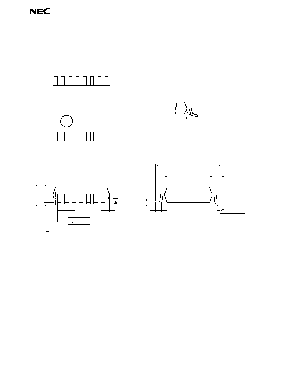
PACKAGE DRAWINGS
16
9
1
8
S
N
S
detail of lead end
C
M
M
A
H
K
L
P
J
I
G
E
F
D
B
ITEM
B
C
H
L
M
16-PIN PLASTIC SSOP (5.72 mm (225))
A
J
D
E
F
G
I
N
MILLIMETERS
0.65 (T.P.)
0.475 MAX.
0.5
±
0.2
6.2
±
0.3
0.10
5.2
±
0.3
0.9
±
0.2
0.22
±
0.8
0.125
±
0.075
1.44
1.565
±
0.235
4.4
±
0.2
0.10
5
∞±
5
∞
P
NOTE
Each lead centerline is located within 0.10 mm of
its true position (T.P.) at maximum material condition.
K
0.17
+
0.08
-
0.07
P16GM-65-225B-4

Data Sheet G13567EJ3V0DS00
17
µ
µ
µ
µ
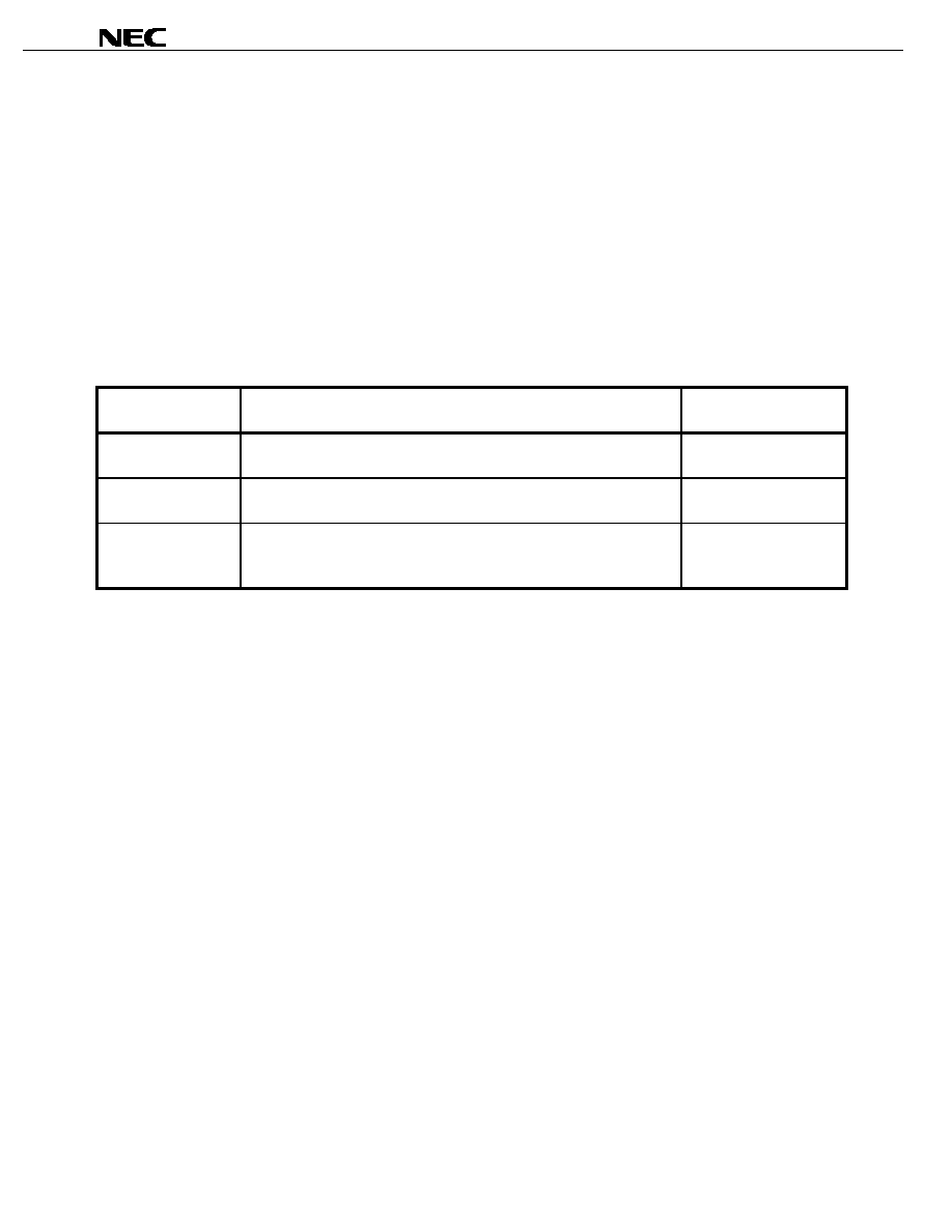
PC1934
B
detail of lead end
K
D
J
M
M
C
16
9
1
8
S
S
A
A'
N
R
F
G
E
P
L
S
H
I
ITEM
B
C
J
16-PIN PLASTIC TSSOP (5.72 mm (225))
D
G
H
I
P
MILLIMETERS
0.65 (T.P.)
0.375 MAX.
1.0
±
0.2
0.24
0.92
4.4
±
0.1
6.4
±
0.2
+
0.06
-
0.04
3
∞+
5
∞
-
3
∞
NOTE
Each lead centerline is located within 0.10 mm of
its true position (T.P.) at maximum material condition.
E
0.09
+
0.06
-
0.04
F
1.01
+
0.09
-
0.06
A
A'
5.0
±
0.1
5.15
±
0.15
K
L
M
N
0.5
0.145
0.10
0.10
+
0.055
-
0.045
R
S
0.25
0.6
±
0.15
S16GR-65-PJG-1
Data Sheet G13567EJ3V0DS00
18
µ
µ
µ
µ
PC1934
6.
RECOMMENDED SOLDERING CONDITIONS
Recommended solder conditions for this product are described below.
For details on recommended soldering conditions, refer to Information Document "Semiconductor Device Mounting
Technology Manual" (C10535E).
For soldering methods and conditions other than those recommended, consult NEC.
Surface Mount Type
µ
µ
µ
µ
PC1934GR-1JG: 16-pin plastic SSOP (5.72 mm (225))
µ
µ
µ
µ
PC1934GR-PJG: 16-pin plastic TSSOP (5.72 mm (225))
Soldering Method
Soldering Conditions
Symbol of Recommended
Conditions
Infrared reflow
Package peak temperature: 235 ∞C, Time: 30 seconds MAX. (210 ∞C MIN.),
Number of times: 3 MAX.
IR35-00-3
VPS
Package peak temperature: 215 ∞C, Time: 40 seconds MAX. (200 ∞C MIN.),
Number of times: 3 MAX.
VP15-00-3
Wave soldering
Soldering bath temperature: 260 ∞C MAX., Time: 10 seconds MAX.,
Number of times: 1,
Preheating temperature: 120 ∞C MAX. (package surface temperature)
WS60-00-1
Caution Do not use two or more soldering methods in combination.

Data Sheet G13567EJ3V0DS00
19
µ
µ
µ
µ
PC1934
NOTES FOR BiCMOS DEVICES
1
PRECAUTION AGAINST ESD FOR SEMICONDUCTORS
Note:
Strong electric field, when exposed to a device, can cause destruction of the gate oxide and
ultimately degrade the device operation. Steps must be taken to stop generation of static electricity
as much as possible, and quickly dissipate it once, when it has occurred. Environmental control
must be adequate. When it is dry, humidifier should be used. It is recommended to avoid using
insulators that easily build static electricity. Semiconductor devices must be stored and transported
in an anti-static container, static shielding bag or conductive material. All test and measurement
tools including work bench and floor should be grounded. The operator should be grounded using
wrist strap. Semiconductor devices must not be touched with bare hands. Similar precautions need
to be taken for PW boards with semiconductor devices on it.
2
HANDLING OF UNUSED INPUT PINS
Note:
No connection for device inputs can be cause of malfunction. If no connection is provided to the
input pins, it is possible that an internal input level may be generated due to noise, etc., hence
causing malfunction. Input levels of devices must be fixed high or low by using a pull-up or pull-
down circuitry. Each unused pin should be connected to V
DD
or GND with a resistor, if it is
considered to have a possibility of being an output pin. All handling related to the unused pins must
be judged device by device and related specifications governing the devices.
3
STATUS BEFORE INITIALIZATION OF BiCMOS DEVICES
Note:
Power-on does not necessarily define initial status of device. Production process of BiCMOS does
not define the initial operation status of the device. Immediately after the power source is turned
ON, the devices with reset function have not yet been initialized. Hence, power-on does not
guarantee out-pin levels, I/O settings or contents of registers. Device is not initialized until the reset
signal is received. Reset operation must be executed immediately after power-on for devices
having reset function.

µ
µ
µ
µ
PC1934
[MEMO]
∑
The information in this document is subject to change without notice. Before using this document, please
confirm that this is the latest version.
∑
No part of this document may be copied or reproduced in any form or by any means without the prior written
consent of NEC Corporation. NEC Corporation assumes no responsibility for any errors which may appear in
this document.
∑
NEC Corporation does not assume any liability for infringement of patents, copyrights or other intellectual property
rights of third parties by or arising from use of a device described herein or any other liability arising from use
of such device. No license, either express, implied or otherwise, is granted under any patents, copyrights or other
intellectual property rights of NEC Corporation or others.
∑
Descriptions of circuits, software, and other related information in this document are provided for illustrative
purposes in semiconductor product operation and application examples. The incorporation of these circuits,
software, and information in the design of the customer's equipment shall be done under the full responsibility
of the customer. NEC Corporation assumes no responsibility for any losses incurred by the customer or third
parties arising from the use of these circuits, software, and information.
∑
While NEC Corporation has been making continuous effort to enhance the reliability of its semiconductor devices,
the possibility of defects cannot be eliminated entirely. To minimize risks of damage or injury to persons or
property arising from a defect in an NEC semiconductor device, customers must incorporate sufficient safety
measures in its design, such as redundancy, fire-containment, and anti-failure features.
∑
NEC devices are classified into the following three quality grades:
"Standard", "Special", and "Specific". The Specific quality grade applies only to devices developed based on a
customer designated "quality assurance program" for a specific application. The recommended applications of
a device depend on its quality grade, as indicated below. Customers must check the quality grade of each device
before using it in a particular application.
Standard: Computers, office equipment, communications equipment, test and measurement equipment,
audio and visual equipment, home electronic appliances, machine tools, personal electronic
equipment and industrial robots
Special: Transportation equipment (automobiles, trains, ships, etc.), traffic control systems, anti-disaster
systems, anti-crime systems, safety equipment and medical equipment (not specifically designed
for life support)
Specific: Aircraft, aerospace equipment, submersible repeaters, nuclear reactor control systems, life
support systems or medical equipment for life support, etc.
The quality grade of NEC devices is "Standard" unless otherwise specified in NEC's Data Sheets or Data Books.
If customers intend to use NEC devices for applications other than those specified for Standard quality grade,
they should contact an NEC sales representative in advance.
M7 98. 8