
DATA SHEET
BIPOLAR ANALOG INTEGRATED CIRCUIT
µ
µ
µ
µ
PC2756TB
MIXER+OSCILLATOR SILICON MMIC FOR FREQUENCY
DOWNCONVERTER OF L BAND WIRELESS RECEIVER
1997
©
Document No. P12807EJ2V0DS00 (2nd edition)
Date Published February 1999 N CP(K)
Printed in Japan
DATA SHEET
The information in this document is subject to change without notice.
The mark
shows major revised points
DESCRIPTION
The
µ
PC2756TB is a silicon monolithic integrated circuit designed as L band frequency downconverter for receiver
stage of wireless systems. The IC consists of mixer and local oscillator. The TB suffix IC which is smaller package
than conventional T suffix IC contributes to reduce your system size.
The
µ
PC2756TB is manufactured using NEC's 20GHz f
T
NESATTM III silicon bipolar process. This process uses
silicon nitride passivation film and gold electrodes. These materials can protect chip surface from external pollution
and prevent corrosion/migration. Thus, this IC has excellent performance, uniformity and reliability.
FEATURES
∑
Wideband operation
: f
RFin
= 0.1 GHz to 2.0 GHz, f
IFout
= 10 MHz to 300 MHz
∑
High-density surface mounting
: 6-pin super mini mold package
∑
Low current consumption
: I
CC
= 6.0 mA TYP. @ V
CC
= 3.0 V
∑
Supply voltage
: V
CC
= 2.7 to 3.3 V
∑
Suppressed spurious signals
: Due to double balanced mixer
∑
Equable output impedance
: Single-end push-pull IF amplifier
∑
Equable temperature-drift oscillator : Differential amplifier type oscillator
APPLICATIONS
∑
Data carrier up to 2.0 GHz MAX.
∑
Wireless LAN up to 2.0 GHz MAX.
ORDERING INFORMATION
Part Number
Marking
Package
Supplying Form
µ
PC2756TB-E3
C1W
6
-
pin super minimold
Embossed tape 8mm wide.
Pin1, 2, 3 face to tape perforation side.
QTY 3kp/reel.
Remark
To order evaluation samples, please contact your local NEC sales office.
(Part number for sample order:
µ
PC2756TB)
Caution Electro-static sensitive devices.
Data Sheet P12807EJ2V0DS00
2
µ
µ
µ
µ
PC2756TB
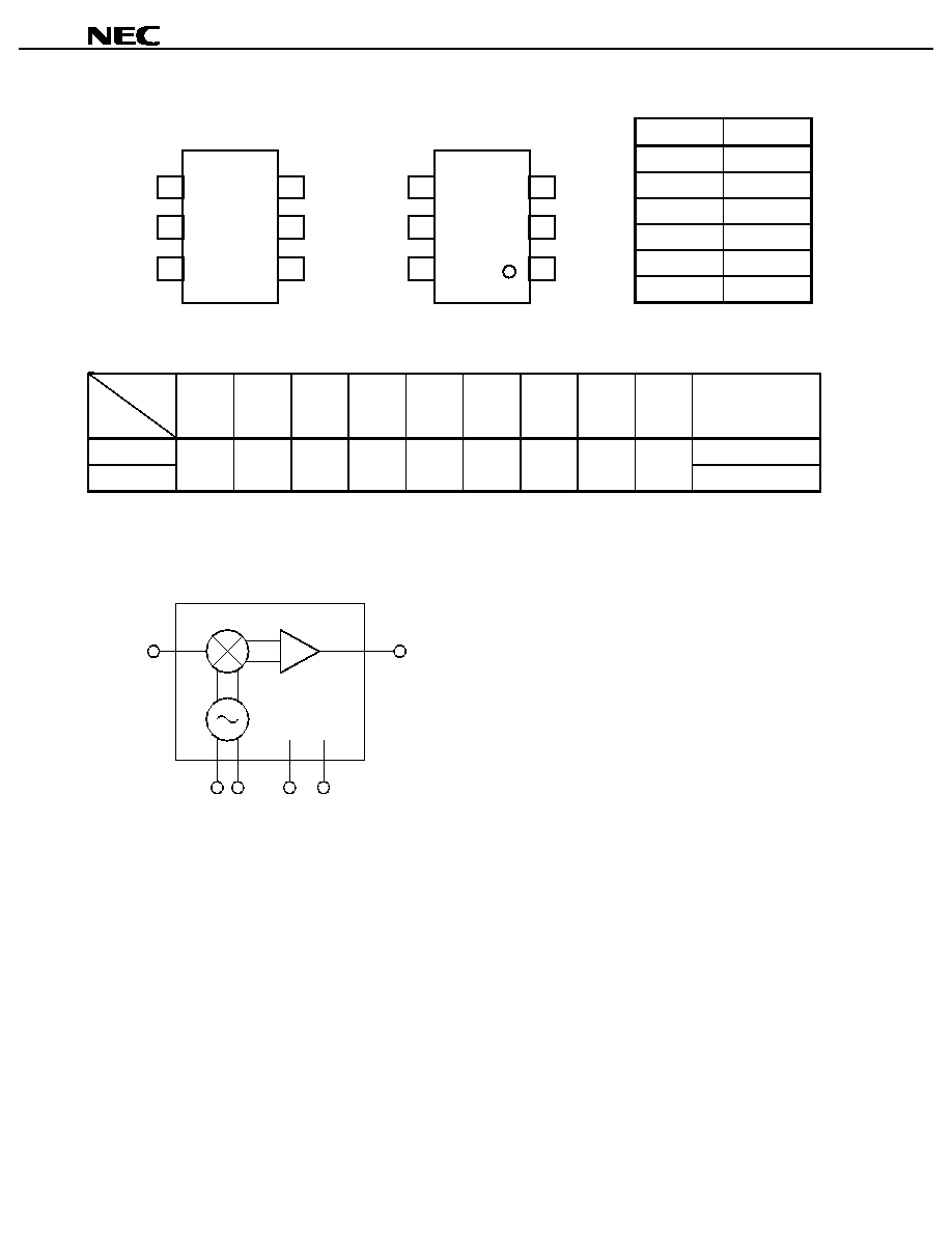
PIN CONNECTIONS
PRODUCT LINE-UP (T
A
= +25 ∞C, V
CC
= 3.0 V, Z
L
= Z
S
= 50
)
Items
V
CC
(V)
I
CC
(mA)
900 MHz
CG
(dB)
1.6 GHz
CG
(dB)
900 MHz
NF
(dB)
1.6 GHz
NF
(dB)
f
RFin
(GHz)
f
IFout
(GHz)
f
OSC
(GHz)
Package
µ
PC2756T
2.7 to 3.3
6.0
14
14
10
13
0.1 to 2.0 10 to 300
to 2.2
6-pin minimold
µ
PC2756TB
6-pin super minimold
Remark Typical performance. Please refer to ELECTRICAL CHARACTERISTICS in detail.
INTERNAL BLOCK DIAGRAM
Pin No.
Pin Name
1
RF
in
2
GND
3
LO
1
4
LO
2
5
V
CC
6
IF
out
Part
Number
3
2
1
4
5
6
C1W
(Top View)
3
2
1
4
5
6
(Bottom View)
RF
input
IF
output
LO
1
LO
2
V
CC
GND
Oscillator
IF amplifier
Mixer
Note Oscillator tank circuit must be externally
attached to LO
1
and LO
2
pins.
Data Sheet P12807EJ2V0DS00
3
µ
µ
µ
µ
PC2756TB
µ
µ
µ
µ
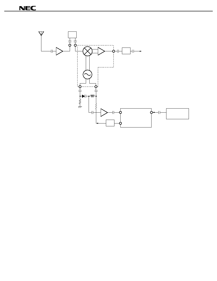
PC2756TB LOCATION EXAMPLE IN THE SYSTEM
PC2745TB
µ
PC2756TB
µ
V
T
BPF
BPF
RX
1st
MIXER
LPF
PLL frequency
synthesizer
Reference
osillator
This document is to be specified for
µ
PC2756TB. For the other part number mentioned in this document, please
refer to the data sheet of each part number.
Data Sheet P12807EJ2V0DS00
4
µ
µ
µ
µ
PC2756TB
6
V
CC
V
CC
3
4
1
V
CC
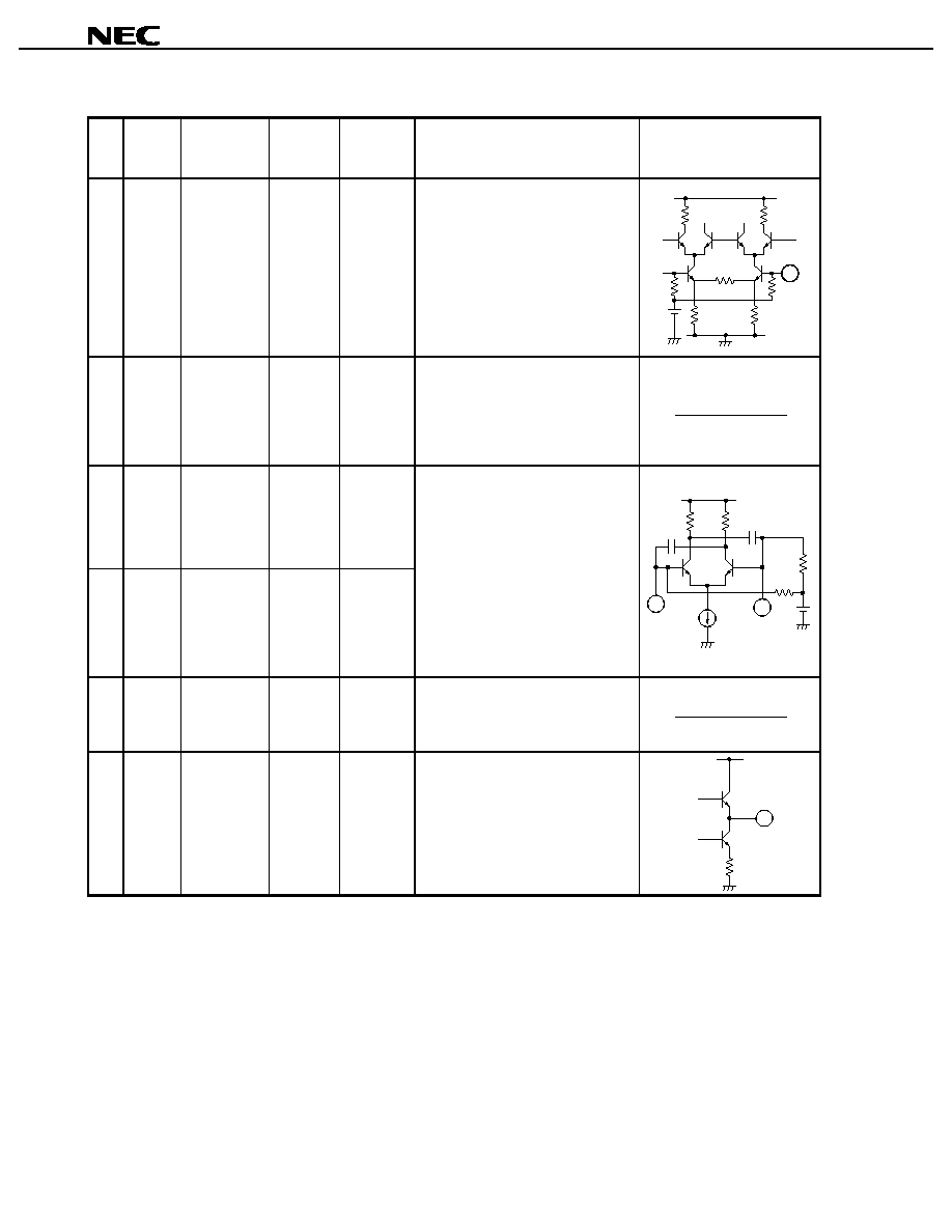
PIN EXPLANATION
Pin
No.
Symbol
Assignment
Applied
Voltage
V
Pin
Voltage
V
Note
Function and Application
Equivalent Circuit
1
RF
in
RF input
≠
1.2
This pin is RF input for mixer designed
as double balance type.
This circuit contributes to suppress
spurious signal with minimum LO and
bias power consumption.
Also this symmetrical circuit can keep
specified performance insensitive to
process-condition distribution.
This pin must be externally coupled to
front stage with capacitor for DC cut.
2
GND
Ground
0
≠
Must be connected to the system
ground with minimum inductance.
Ground pattern on the board should
be formed as wide as possible.
(Track length should be kept as short
as possible.)
3
4
LO
1
LO
2
Local oscillator
base collector
Local oscillator
base collector
≠
≠
1.2
1.2
These pins are both base-collector of
oscillator. This oscillator is designed
as differential amplifier type.
3 pin and 4 pin should be externally
equipped with tank resonator circuit in
order to oscillate with feedback loop.
Also this symmetrical circuit can keep
specified performance insensitive to
process-condition distribution.
Each pin must be externally coupled
to tank circuit with capacitor for DC
cut.
5
V
CC
Power supply
2.7 to 3.3
≠
Supply voltage 3.0
±
0.3 V for
operation. Must be connected bypass
capacitor (e.g. 1 000 pF) to minimize
ground impedance.
6
IF out
IF output
≠
1.7
This pin is output from IF buffer
amplifier designed as single-ended
push-pull type.
This pin is assigned for emitter
follower output with low-impedance.
This pin must be externally coupled to
next stage with capacitor for DC cut.
Note Pin voltage is measured at V
CC
= 3.0 V
APPLICATION
This IC is guaranteed on the test circuit constructed with 50
equipment and transmission line. This IC, however,
does not have 50
input/output impedance, but electrical characteristics such as conversion gain and
intermodulation distortion are described herein on these conditions without impedance matching. So, you should
understand that conversion gain and intermodulation distortion at input level will vary when you improve VS of RF
input with external circuit (50
termination or impedance matching).
External circuits of the IC are explained in a following application note.
∑
To RF and IF port : Application Note "Usage and Application Characteristics of
µ
PC2757T,
µ
PC2758T and
µ
PC8112T, 3-V Power Supply, 1.9-GHz Frequency Down Converter ICs for Cellular/Cordless Telephone and
Portable Wireless Communication" (Document No. P11997E)
Data Sheet P12807EJ2V0DS00
5
µ
µ
µ
µ
PC2756TB
ABSOLUTE MAXIMUM RATINGS
Parameter
Symbol
Conditions
Rating
Unit
Supply Voltage
V
CC
T
A
= +25 ∞C
5.5
V
Power Dissipation
P
D
Mounted on double sided copper clad
50
◊
50
◊
1.6 mm epoxy glass PWB (T
A
= +85 ∞C)
200
mW
Operating Ambient Temperature
T
A
≠40 to +85
∞C
Storage Temperature
T
stg
≠55 to +150
∞C
RECOMMENDED OPERATING RANGE
Parameter
Symbol
MIN.
TYP.
MAX.
Unit
Supply Voltage
V
CC
2.7
3.0
3.3
V
Operating Ambient Temperature
T
A
≠40
+25
+85
∞C
ELECTRICAL CHARACTERISTICS (T
A
= +25 ∞C, V
CC
= 3.0 V, Z
L
= Z
S
= 50
, Test circuit)
Parameter
Symbol
Conditions
MIN.
TYP.
MAX.
Unit
Circuit Current
I
CC
No input signals
3.5
6.0
8.0
mA
RF Frequency Response
f
RFin
CG
(CG1 ≠3 dB)
f
IFout
= 150 MHz constant
0.1
≠
2.0
GHz
IF Frequency Response
f
IFout
CG
(CG1 ≠3 dB)
f
RFin
= 0.9 GHz constant
10
≠
300
MHz
Conversion Gain 1
CG1
f
RFin
= 0.9 GHz, f
IFout
= 150 MHz
P
RFin
= ≠40 dBm
11
14
17
dB
Conversion Gain 2
CG2
f
RFin
= 1.6 GHz, f
IFout
= 20 MHz
P
RFin
= ≠40 dBm
11
14
17
dB
Single Sideband Noise Figure 1
NF1
f
RFin
= 0.9 GHz, f
IFout
= 150 MHz
≠
10
13
dB
Single Sideband Noise Figure 2
NF2
f
RFin
= 1.6 GHz, f
IFout
= 20 MHz
≠
13
16
dB
Maximum IF Output Level 1
P
O (SAT) 1
f
RFin
= 0.9 GHz, f
IFout
= 150 MHz
P
RFin
= ≠10 dBm
≠11
≠8
≠
dBm
Maximum IF Output Level 2
P
O (SAT) 2
f
RFin
= 1.6 GHz, f
IFout
= 20 MHz
P
RFin
= ≠10 dBm
≠15
≠12
≠
dBm
STANDARD CHARACTERISTICS FOR REFERENCE (Unless otherwise specified, T
A
= +25 ∞C, V
CC
= 3.0 V,
Z
L
= Z
S
= 50
)
Parameter
Symbol
Conditions
Reference
Unit
Output 3rd Order Intercept Point
OIP
3
f
RFin
= 0.8 to 2.0 GHz, f
IFout
= 0.1 GHz, Cross point IP.
+4.0
dBm
Phase Noise
PN
f
OSC
= 1.9 GHz
Note
≠68
dBc/Hz
LO Leakage at RF Pin
LO
rf
f
LOin
= 0.8 to 2.0 GHz
≠35
dB
LO Leakage at IF Pin
LO
if
f
LOin
= 0.8 to 2.0 GHz
≠23
dB
Maximum Oscillating Frequency
f
OSCMAX.
VaractorDi: 1SV210, L: 7 nH
Note
2.2
GHz
Note On application circuit example.

Data Sheet P12807EJ2V0DS00
6
µ
µ
µ
µ
PC2756TB
SCHEMATIC SUPPLEMENT FOR RF, IF SPECIFICATIONS
CG1
CG1
-
3 dB
0.1
0.9
2.0
RF Frequency f
RF
(GHz)
Guaranteed gain level
f
IF
= 150 MHz
P
RFin
=
-
40 dBm
RF Frequency Response
Conversion Gain CG (dB)
CG1
CG1
-
3 dB
10
150
300
IF Frequency f
IF
(GHz)
Guaranteed gain level
f
RF
= 0.9 GHz
P
RFin
=
-
40 dBm
IF Frequency Response
Conversion Gain CG (dB)
MIN.
TYP.
MAX.
Unit
CG1
11
14
17
dB
CG1-3 dB
8
11
14
dB
Data Sheet P12807EJ2V0DS00
7
µ
µ
µ
µ
PC2756TB
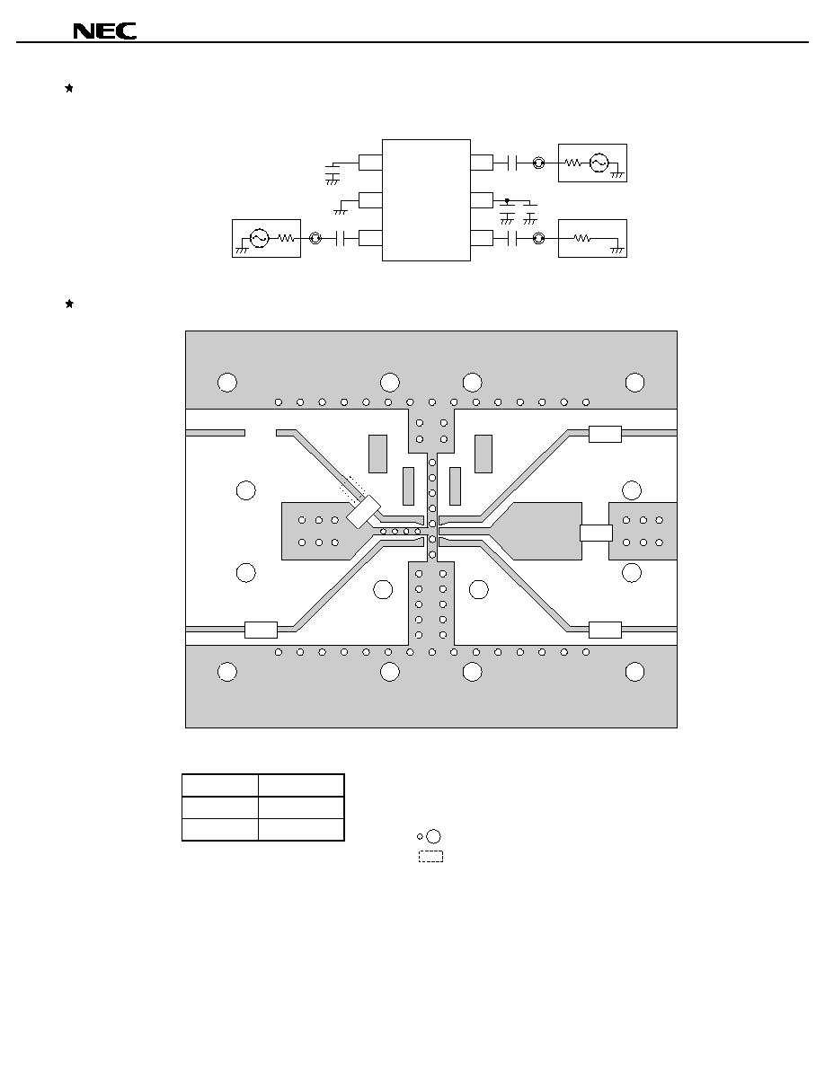
TEST CIRCUIT
LO
1
GND
RF
in
LO
2
V
CC
IF
out
3
2
1
4
5
6
50
1 000 pF
C
3
3 300 pF
3 V
3 300 pF
C
5
C
4
1 000 pF
C
2
C
1
1 000 pF
(Top View)
Signal Generator
50
Signal Generator
50
Spectram Analyzer
ILLUSTRATION OF THE TEST CIRCUIT ASSEMBLED ON EVALUATION BOARD
C
1
C
3
C
4
GND
V
CC
LO
1
RF
input
LO
2
IF
output
C
5
C
2
Notes
(1) 35
◊
42
◊
0.4 mm double copper clad polyimide board.
(2) Back side: GND pattern
(3) Solder plated on pattern
(4) : Through holes
(5)
pattern should be removed on this testing.
COMPONENT LIST
No.
Value
C
1
to C
3
1 000 pF
C
4
, C
5
3 300 pF
Data Sheet P12807EJ2V0DS00
8
µ
µ
µ
µ
PC2756TB
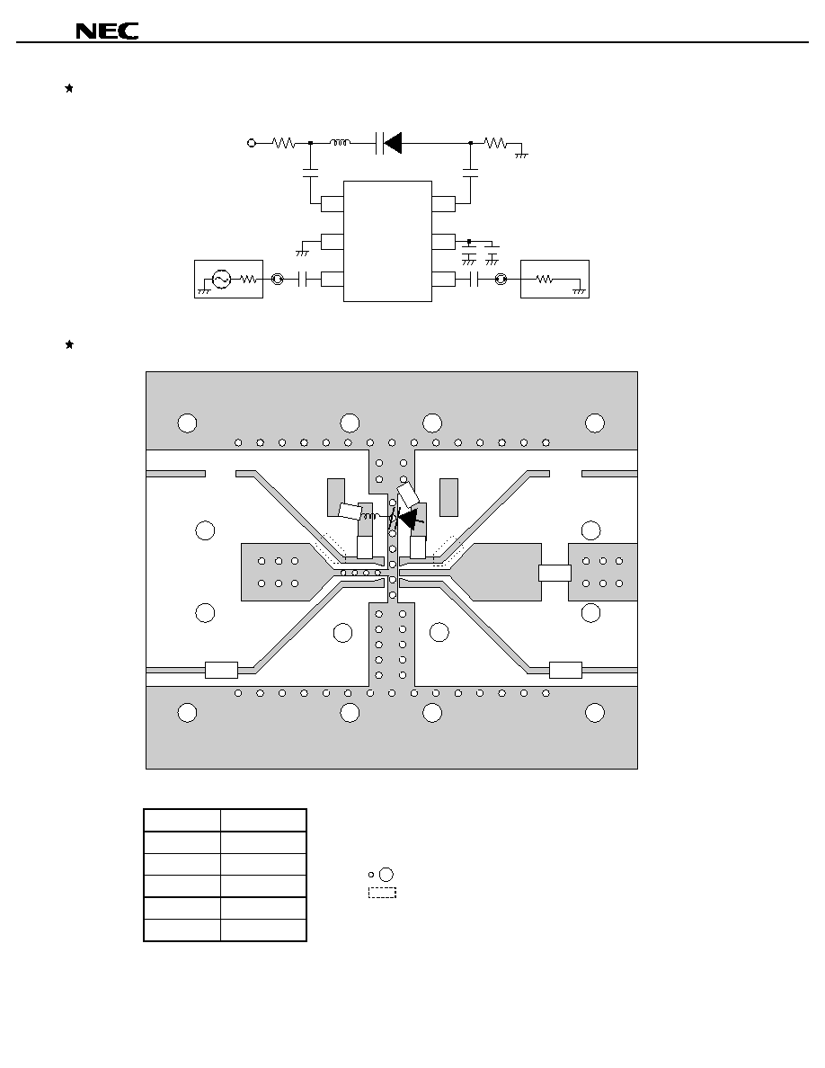
COMPONENT LIST
No.
Value
C
1
to C
3
1 000 pF
C
4
, C
5
3 300 pF
R
1
, R
2
15 k
L
5 nH to 30 nH
HVU12
APPLICATION CIRCUIT EXAMPLE
LO
1
GND
RF
in
LO
2
V
CC
IF
out
3
2
1
4
5
6
1 000 pF
C
3
3 300 pF
3 V
3 300 pF
C
5
C
4
1 000 pF
C
2
C
1
1 000 pF
(Top View)
15 k
V
T
bias
R
2
R
1
15 k
L
5 nH
30 nH
HVU12
50
Signal Generator
50
Spectram Analyzer
ILLUSTRATION OF THE APPLICATION CIRCUIT ASSEMBLED ON EVALUATION BOARD
GND
V
CC
RF
input
IF
output
C
1
C
4
R
2
R
1
V
T
C
5
C
3
C
2
The application circuits and their parameters are for reference only and are not intended for use in actual design-ins.
Notes
(1) 35
◊
42
◊
0.4 mm double copper clad polyimide board.
(2) Back side: GND pattern
(3) Solder plated on pattern
(4) : Through holes
(5) pattern should be removed on this testing.
Data Sheet P12807EJ2V0DS00
9
µ
µ
µ
µ
PC2756TB
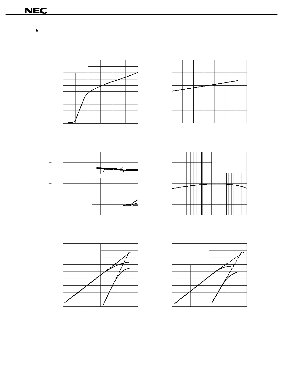
TYPICAL CHARACTERISTICS (T
A
= +25
∞
∞
∞
∞
C)
-
ON THE TEST CIRCUIT
-
CIRCUIT CURRENT vs. SUPPLY VOLTAGE
Supply Voltage V
CC
(V)
Circuit Current I
CC
(mA)
0
CONVERSION GAIN, SSB NOISE FIGURE vs. RF INPUT FREQUENCY
RF Input Frequency f
RFin
(GHz)
Single Side Band Noise Figure SSBNF (dB)
10
IF OUTPUT LEVEL, IM
3
vs. RF INPUT LEVEL
RF Input Level P
RFin
(dBm)
-
70
-
80
2
2
4
6
8
10
4
6
20
25
1.0
0.5
1.5
2.0
-
40
-
10
+
20
-
40
-
20
0
1
3
5
Conversion Gain CG (dB)
15
5
15
20
10
P
RFin
= ≠55 dBm
P
L0in
= ≠10 dBm
f
IF
= 150 MHz
(Low-Side LO)
NF
f
RF1
= 900 MHz
f
RF2
= 905 MHz
f
LO
= 800 MHz
V
CC
= 3.0 V
+
10
0
-
30
-
20
-
50
-
60
-
60
CG
V
CC
= 3.3 V
V
CC
= 2.7 V
V
CC
= 3.0 V
CIRCUIT CURRENT vs. OPERATING AMBIENT TEMPERATURE
Operating Ambient Temperature T
A
(
∞
C)
Circuit Current I
CC
(mA)
-
40
CONVERSION GAIN vs. IF OUTPUT FREQUENCY
IF Output Frequency f
IFout
(MHz)
Conversion Gain CG (dB)
0
1
-
20
0
+
20
+
80
+
100
2
4
6
8
10
10
5
20
15
30
+
40
+
60
0
No input signal
V
CC
= 3.0 V
25
2
5
10
20
50
100
300
V
CC
= 3.0 V
P
RFin
= ≠55 dBm
P
L0in
= ≠10 dBm
f
RF
= 1.6 GHz
IF coupling = 0.1 F
µ
IF OUTPUT LEVEL, IM
3
vs. RF INPUT LEVEL
-
70
-
40
-
10
+
20
f
RF1
= 2.0 GHz
f
RF2
= 2.005 GHz
f
LO
= 1.9 GHz
V
CC
= 3.0 V
+
10
0
-
30
-
20
-
50
-
60
-
80
-
40
-
20
0
-
60
IF
Output Level
P
IFout
(dBm)
3rd Order Intermodulation Distortion
IM
3
(dBm)
RF Input Level P
RFin
(dBm)
IF Output Level P
IFout
(dBm)
3rd Order Intermodulation Distortion IM
3
(dBm)
No input signal

Data Sheet P12807EJ2V0DS00
10
µ
µ
µ
µ
PC2756TB
-
ON THE APPLICATION CIRCUIT
-
LO LEAKAGE AT IF PIN vs. LOCAL INPUT FREQUENCY
Local Input Frequency f
LO
(GHz)
Local Leakage at IF Output Pin LO
if
(dBm)
1.2
1.0
1.4
1.6
-
60
-
40
-
30
-
50
V
CC
= 3.0 V
P
L0in
=
-
10 dBm
0
-
10
-
20
0.8
LO LEAKAGE AT RF PIN vs. LOCAL INPUT FREQUENCY
1.6
1.8
-
60
-
40
-
30
-
50
2.0
0
-
10
-
20
1.4
Local Input Frequency f
LO
(GHz)
Local Leakage at RF Pin LO
rf
(dBm)
V
CC
= 3.0 V
P
L0in
= -10 dBm
Data Sheet P12807EJ2V0DS00
11
µ
µ
µ
µ
PC2756TB
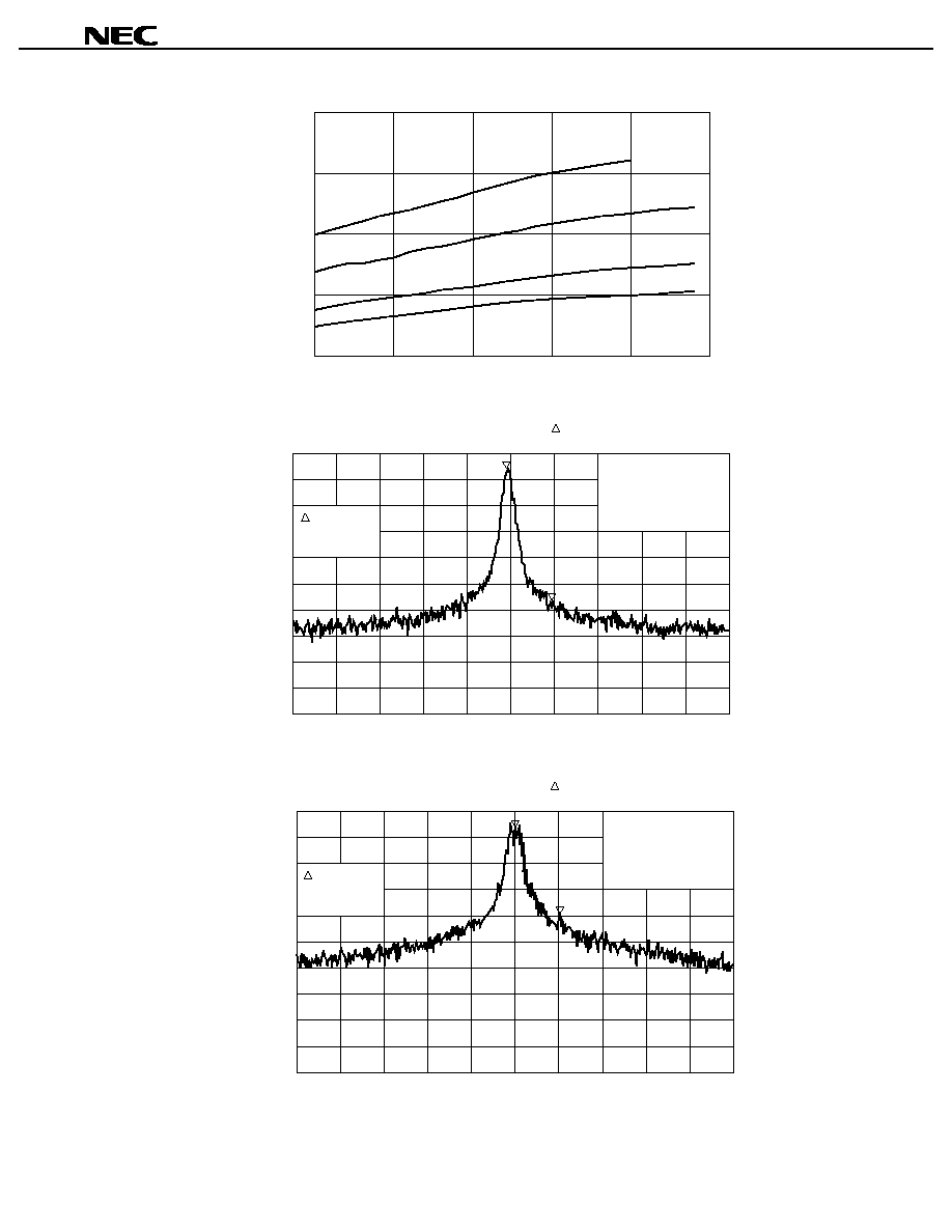
VCO OSCILLATION FREQUENCY vs. TUNING VOLTAGE
2.5
2.0
1.5
1.0
0.5
0
5
10
15
20
25
Tuning Voltage V
tu
(V)
VCO Oscillation Frequency f
VCO
(GHz)
L = 7 nH
L = 15 nH
L = 30 nH
L = 50 nH
ATTEN 10 dB
RL
-
40.0 dBm
10 dB /
MKR
-
53.16 dB
10.0 kHz
V
CC
= 3 V
Vtune = 3 V
T
A
=
+
25
∞
C
Monitor at pin 6
MKR
10.0 kHz
-
53.16 dB
CENTER 774.425 8 MHz
RBW 1.0 kHz ++ VBW 100 Hz
SPAN 100.0 kHz
SWP 3.0 s
VCO Phase Noise (f
VCO
= 774.425 8 MHz center)
ATTEN 10 dB
RL ≠40.0 dBm
10 dB /
MKR ≠40.34 dB
10.2 kHz
MKR
10.2 kHz
≠40.34 dB
CENTER 1.639 194 2 GHz
RBW 1.0 kHz
++
VBW 100 Hz
SPAN 100.0 kHz
SWP 3.0 s
VCO Phase Noise (f
VCO
= 1.639 194 2 GHz center)
D
K
D
K
V
CC
= 3 V
Vtune = 3 V
T
A
= +25
∞
C
Monitor at pin 6
Data Sheet P12807EJ2V0DS00
12
µ
µ
µ
µ
PC2756TB
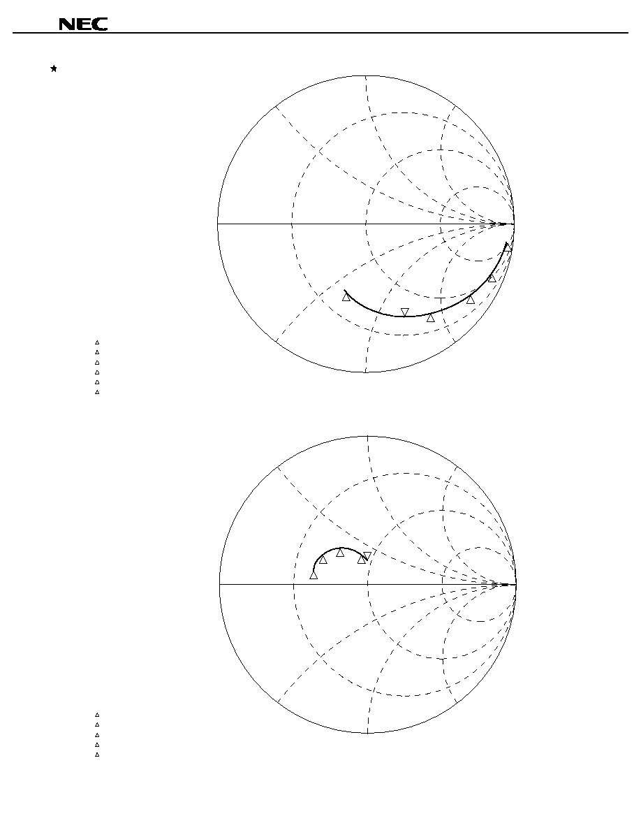
S-PARAMETOR
RF Port
V
CC
= 3.0 V
1
: 100 MHz 519.8
-
j 1.1
2
: 500 MHz 59.3
-
j 281.0
3
: 900 MHz 38.3
-
j 157.0
4
: 1 500 MHz 31.5
-
j 90.1
5
: 1 900 MHz 28.5
-
j 67.9
6
: 3 000 MHz 25.7
-
j 31.7
IF Port
V
CC
= 3.0 V
1
: 50 MHz 22.5
+
j 6.1
2
: 80 MHz 24.2
+
j 11.3
3
: 130 MHz 30.2
+
j 16.6
4
: 240 MHz 42.6
+
j 17.5
5
: 300 MHz 46.6
+
j 15.6
1
START 0.100000000 GHz
STOP 3.100000000 GHz
2
3
4
6
5
1
START 0.050000000 GHz
STOP 0.300000000 GHz
3
2
4
5
Data Sheet P12807EJ2V0DS00
13
µ
µ
µ
µ
PC2756TB
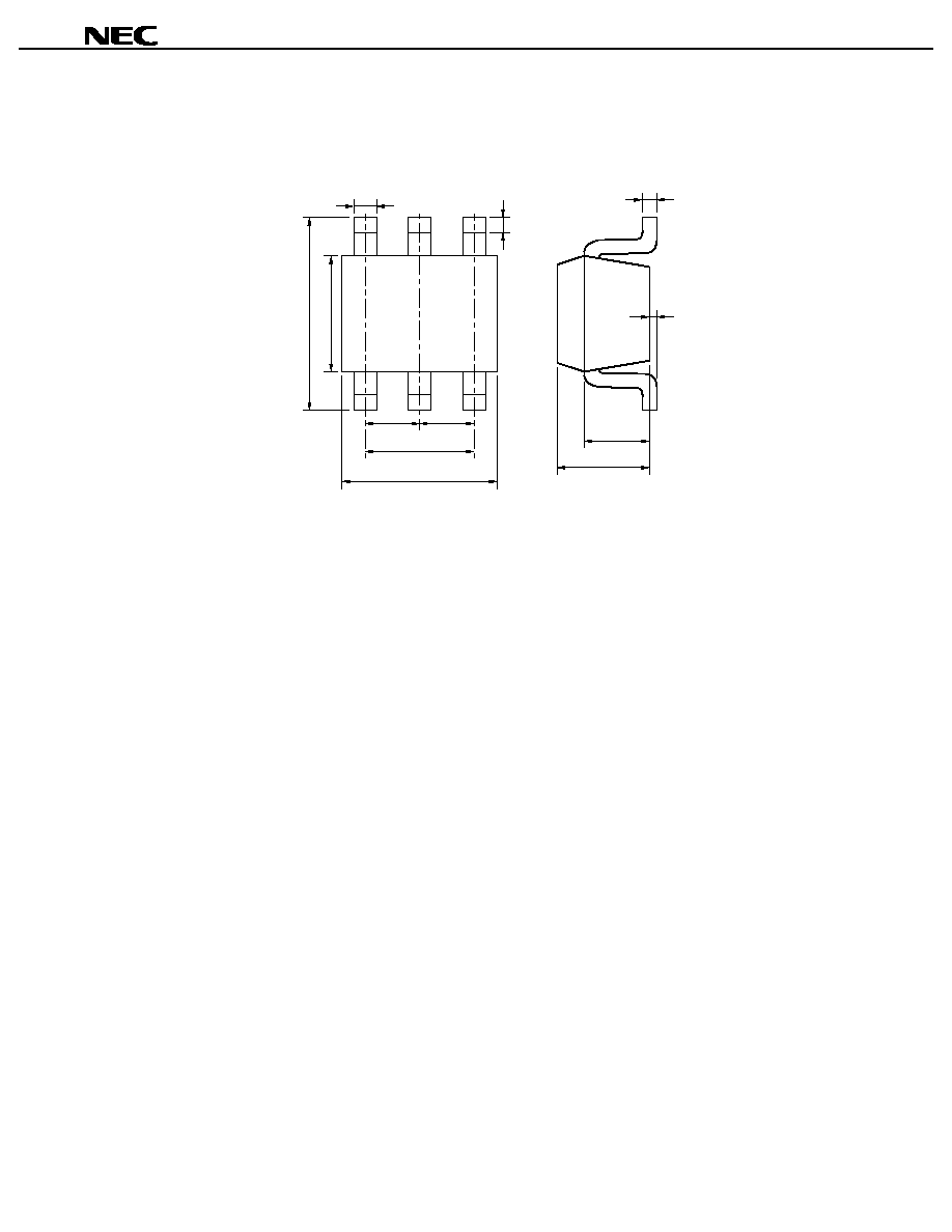
PACKAGE DIMENSIONS
6 pin super minimold (unit: mm)
2.0±0.2
1.3
0.65
0.65
1.25±0.1
2.1±0.1
0.2
+0.1
≠0
0.1 MIN.
0.7
0.9±0.1
0 to 0.1
0.15
+0.1
≠0
Data Sheet P12807EJ2V0DS00
14
µ
µ
µ
µ
PC2756TB
NOTE ON CORRECT USE
(1) Observe precautions for handling because of electro-static sensitive devices.
(2) Form a ground pattern as widely as to minimize ground impedance (to prevent abnormal oscillation).
(3) Keep the track length between the ground pins as short as possible.
(4) Connect a bypass capacitor (example 1 000 pF) to the V
CC
pin.
(5) To construct oscillator, tank circuit must be externally attached to pin 3 and 4.
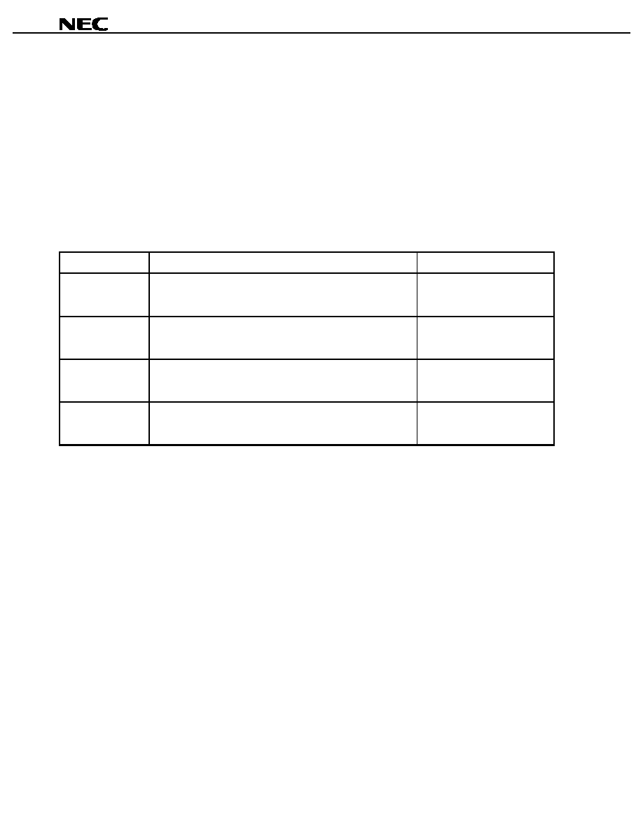
RECOMMENDED SOLDERING CONDITIONS
This product should be soldered under the following recommended conditions. For soldering methods and
conditions other than those recommended below, contact your NEC sales representative.
µ
µ
µ
µ
PC2756TB
Soldering Method
Soldering Conditions
Recommended Condition Symbol
Infrared Reflow
Package peak temperature: 235 ∞C or below
Time: 30 seconds or less (at 210 ∞C)
Count: 3, Exposure limit
Note
: None
IR35-00-3
VPS
Package peak temperature: 215 ∞C or below
Time: 40 seconds or less (at 200 ∞C)
Count: 3, Exposure limit
Note
: None
VP15-00-3
Wave Soldering
Soldering bath temperature: 260 ∞C or below
Time: 10 seconds or less
Count: 1, Exposure limit
Note
: None
WS60-00-1
Partial Heating
Pin temperature: 300 ∞C
Time: 3 seconds or less (per side of device)
Exposure limit
Note
: None
≠
Note After opening the dry pack, keep it in a place below 25 ∞C and 65 % RH for the allowable storage period.
Caution Do not use different soldering methods together (except for partial heating).
For details of recommended soldering conditions for surface mounting, refer to information document
SEMICONDUCTOR DEVICE MOUNTING TECHNOLOGY MANUAL (C10535E).

Data Sheet P12807EJ2V0DS00
15
µ
µ
µ
µ
PC2756TB
[MEMO]

µ
µ
µ
µ
PC2756TB
ATTENTION
OBSERVE PRECAUTIONS
FOR HANDLING
ELECTROSTATIC
SENSITIVE
DEVICES
The application circuits and their parameters are for reference only and are not intended for use in actual design-ins.
NESAT (NEC Silicon Advanced Technology) is a trademark of NEC Corporation.
No part of this document may be copied or reproduced in any form or by any means without the prior written
consent of NEC Corporation. NEC Corporation assumes no responsibility for any errors which may appear in
this document.
NEC Corporation does not assume any liability for infringement of patents, copyrights or other intellectual property
rights of third parties by or arising from use of a device described herein or any other liability arising from use
of such device. No license, either express, implied or otherwise, is granted under any patents, copyrights or other
intellectual property rights of NEC Corporation or others.
While NEC Corporation has been making continuous effort to enhance the reliability of its semiconductor devices,
the possibility of defects cannot be eliminated entirely. To minimize risks of damage or injury to persons or
property arising from a defect in an NEC semiconductor device, customers must incorporate sufficient safety
measures in its design, such as redundancy, fire-containment, and anti-failure features.
NEC devices are classified into the following three quality grades:
"Standard", "Special", and "Specific". The Specific quality grade applies only to devices developed based on a
customer designated "quality assurance program" for a specific application. The recommended applications of
a device depend on its quality grade, as indicated below. Customers must check the quality grade of each device
before using it in a particular application.
Standard: Computers, office equipment, communications equipment, test and measurement equipment,
audio and visual equipment, home electronic appliances, machine tools, personal electronic
equipment and industrial robots
Special: Transportation equipment (automobiles, trains, ships, etc.), traffic control systems, anti-disaster
systems, anti-crime systems, safety equipment and medical equipment (not specifically designed
for life support)
Specific: Aircrafts, aerospace equipment, submersible repeaters, nuclear reactor control systems, life
support systems or medical equipment for life support, etc.
The quality grade of NEC devices is "Standard" unless otherwise specified in NEC's Data Sheets or Data Books.
If customers intend to use NEC devices for applications other than those specified for Standard quality grade,
they should contact an NEC sales representative in advance.
Anti-radioactive design is not implemented in this product.
M4 96. 5