Document Outline
- COVER
- DESCRIPTION
- FEATURES
- APPLICATIONS
- ORDERING INFORMATION
- PIN CONNECTIONS
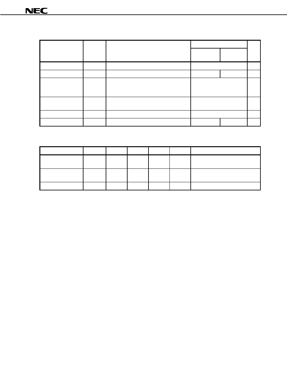
- PRODUCT LINE-UP (TA = +25 degrees, VCC = Vout = 3.0 V, ZL = ZS = 50 ohm)
- SYSTEM APPLICATION EXAMPLE
- PIN EXPLANATION
- ABSOLUTE MAXIMUM RATINGS
- RECOMMENDED OPERATING CONDITIONS
- ELECTRICAL CHARACTERISTICS (TA = +25 degrees, VCC = Vout = 3.0 V, ZL = ZS = 50 ohm)
- STANDARD CHARACTERISTICS FOR REFERENCE (TA = +25 degrees, VCC = Vout = 3.0 V, ZL = ZS = 50 ohm)
- TEST CIRCUIT
- COMPONENTS OF TEST CIRCUIT FOR MEASURING ELECTRICAL CHARACTERISTICS
- EXAMPLE OF ACTUAL APPLICATION COMPONENTS
- INDUCTOR FOR THE OUTPUT PIN
- CAPACITORS FOR THE VCC, INPUT, AND OUTPUT PINS
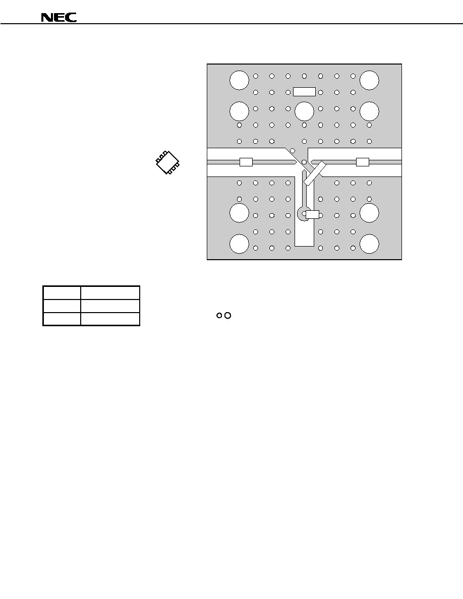
- ILLUSTRATION OF THE TEST CIRCUIT ASSEMBLED ON EVALUATION BOARD
- COMPONENT LIST
- TYPICAL CHARACTERISTICS (Unless otherwise specified, TA = +25 degrees)
- S-PARAMETER (TA = +25 degrees, VCC = Vout = 3.0 V)
- TYPICAL S-PARAMETER VALUES (TA = +25 degrees)
- TYPICAL CHARACTERISTICS (Unless otherwise specified, TA = +25 degrees)
- S-PARAMETER (TA = +25 degrees, VCC = Vout = 3.0 V)
- TYPICAL S-PARAMETER VALUES (TA = +25 degrees)
- TYPICAL CHARACTERISTICS (Unless otherwise specified, TA = +25 degrees)
- S-PARAMETER (TA = +25 degrees, VCC = Vout = 3.0 V)
- TYPICAL S-PARAMETER VALUES (TA = +25 degrees)
- PACKAGE DIMENSIONS
- NOTES ON CORRECT USE
- RECOMMENDED SOLDERING CONDITIONS
Caution Electro-static sensitive devices
The information in this document is subject to change without notice. Before using this document, please
confirm that this is the latest version.
Not all devices/types available in every country. Please check with local NEC representative for
availability and additional information.
3 V, SUPER MINIMOLD SILICON MMIC
MEDIUM OUTPUT POWER AMPLIFIER
FOR MOBILE COMMUNICATIONS
Document No. P12710EJ2V0DS00 (2nd edition)
Date Published June 1999 N CP(K)
Printed in Japan
DATA SHEET
BIPOLAR ANALOG INTEGRATED CIRCUITS
µ
µ
µ
µ
PC2762TB,
µ
µ
µ
µ
PC2763TB,
µ
µ
µ
µ
PC2771TB
1997, 1999
©
The mark
shows major revised points.
DESCRIPTION
The
µ
PC2762TB,
µ
PC2763TB and
µ
PC2771TB are silicon monolithic integrated circuits designed as amplifier for
mobile communications. Each of the ICs is packaged in super minimold package which is smaller than conventional
minimold. The
µ
PC2762TB,
µ
PC2763TB and
µ
PC2771TB have compatible pin connections and performance to
µ
PC2762T,
µ
PC2763T and
µ
PC2771T of conventional minimold version. So, in the case of reducing your system
size,
µ
PC2762TB,
µ
PC2763TB and
µ
PC2771TB are suitable to replace from
µ
PC2762T,
µ
PC2763T and
µ
PC2771T.
These IC is manufactured using NEC's 20 GHz f
T
NESATTMIII silicon bipolar process. This process uses silicon
nitride passivation film and gold electrodes. These materials can protect chip surface from external pollution and
prevent corrosion/migration. Thus, this IC has excellent performance, uniformity and reliability.
FEATURES
∑
High-density surface mounting : 6-pin super minimold package (2.0
◊
1.25
◊
0.9 mm)
∑
Supply voltage
: V
CC
= 2.7 to 3.3 V
∑
Medium output power
:
µ
PC2762TB: P
O(1 dB)
= +8.0 dBm TYP. @ 0.9 GHz
µ
PC2763TB: P
O(1 dB)
= +9.5 dBm TYP. @ 0.9 GHz
µ
PC2771TB: P
O(1 dB)
= +11.5 dBm TYP. @ 0.9 GHz
∑
Power gain
:
µ
PC2762TB: G
P
= 13 dB TYP. @ 0.9 GHz
µ
PC2763TB: G
P
= 20 dB TYP. @ 0.9 GHz
µ
PC2771TB: G
P
= 21 dB TYP. @ 0.9 GHz
APPLICATIONS
∑
Buffer amplifiers for mobile telephones :
µ
PC2762TB,
µ
PC2763TB
∑
PA driver for PDC800M
:
µ
PC2771TB
ORDERING INFORMATION
Part Number
Package
Marking
Supplying Form
µ
PC2762TB-E3
C1Z
µ
PC2763TB-E3
6-pin super minimold
C2A
µ
PC2771TB-E3
C2H
Embossed tape 8 mm wide.
1, 2, 3 pins face to perforation side of the tape.
Qty 3 kp/reel.
Remark To order evaluation samples, please contact your local NEC sales office.
(Part number for sample order:
µ
PC2762TB,
µ
PB2763TB,
µ
PC2771TB)
Data Sheet P12710EJ2V0DS00
2
µ
µ
µ
µ
PC2762TB,
µ
µ
µ
µ
PC2763TB,
µ
µ
µ
µ
PC2771TB
PIN CONNECTIONS
Marking is an example of
µ
PC2762TB
PRODUCT LINE-UP (T
A
= +25 ∞C, V
CC
= V
out
= 3.0 V, Z
L
= Z
S
= 50
)
Part No.
f
u
(GHz)
P
O (1 dB)
(dBm)
P
O (sat)
(dBm)
G
P
(dB)
I
CC
(mA)
Package
Marking
µ
PC2762T
2.9
+8.0
+9.0
13
26.5
6-pin minimold
µ
PC2762TB
6-pin super minimold
µ
PC2763T
2.7
+9.5
+11.0
20
27.0
6-pin minimold
µ
PC2763TB
6-pin super minimold
µ
PC2771T
2.2
+11.5
+12.5
21
36.0
6-pin minimold
µ
PC2771TB
6-pin super minimold
Remark Typical performance. Please refer to ELECTRICAL CHARACTERISTICS in detail.
Notice The package size distinguishes between minimold and super minimold.
C2H
Pin No.
Pin Name
1
INPUT
2
GND
3
GND
4
OUTPUT
5
GND
6
V
CC
4
5
6
3
2
1
(Top View)
C1Z
3
2
1
4
5
6
(Bottom View)
C1Z
C2A
Data Sheet P12710EJ2V0DS00
3
µ
µ
µ
µ
PC2762TB,
µ
µ
µ
µ
PC2763TB,
µ
µ
µ
µ
PC2771TB
SYSTEM APPLICATION EXAMPLE
Digital cellular telephone
DEMO
PLL
Phase
shifter
0
∞
90
∞
I
Q
I
Q
PA
SW
TX
RX
PLL
˜
N
µ
PC2762TB
or
PC2763TB
PC2771TB
µ
µ
Note The insertion point is different due to the specifications of conjunct devices.
For conjunction with your devices, refer to the data sheets to confirm their conbination.
Data Sheet P12710EJ2V0DS00
4
µ
µ
µ
µ
PC2762TB,
µ
µ
µ
µ
PC2763TB,
µ
µ
µ
µ
PC2771TB
PIN EXPLANATION
Pin
No.
Pin Name
Applied
Voltage
(V)
Pin
Voltage
(V)
Note
Function and Applications
Internal Equivalent Circuit
1
INPUT
≠
1.31
1.01
0.97
Signal input pin. A internal
matching circuit, configured with
resistors, enables 50
connection over a wide band.
A multi-feedback circuit is
designed to cancel the
deviations of h
FE
and resistance.
This pin must be coupled to
signal source with capacitor for
DC cut.
4
OUTPUT
Voltage
as same
as V
CC
through
external
inductor
≠
Signal output pin. The inductor
must be attached between V
CC
and output pins to supply
current to the internal output
transistors.
6
V
CC
2.7 to 3.3
≠
Power supply pin, which biases
the internal input transistor.
This pin should be externally
equipped with bypass capacitor
to minimize its impedance.
2
3
5
GND
0
≠
Ground pin. This pin should be
connected to system ground
with minimum inductance.
Ground pattern on the board
should be formed as wide as
possible.
All the ground pins must be
connected together with wide
ground pattern to decrease
impedance difference.
6
4
1
5
*
* PC2762TB does not have
this capacitance.
µ
2
3
GND
GND
Note
Pin voltage is measured at V
CC
= 3.0 V. Above:
µ
PC2762TB, Center:
µ
PC2763TB, Below:
µ
PC2771TB.
Data Sheet P12710EJ2V0DS00
5
µ
µ
µ
µ
PC2762TB,
µ
µ
µ
µ
PC2763TB,
µ
µ
µ
µ
PC2771TB
ABSOLUTE MAXIMUM RATINGS
Ratings
Parameter
Symbol
Conditions
µ
PC2762TB
µ
PC2763TB
µ
PC2771TB
Unit
Supply Voltage
V
CC
T
A
= +25
∞
C, pin 4 and 6
3.6
V
Total Circuit Current
I
CC
T
A
= +25
∞
C
70
77.7
mA
Power Dissipation
P
D
Mounted on double copper clad
50
◊
50
◊
1.6 mm epoxy glass PWB
T
A
= +85
∞
C
200
mW
Operating Ambient
Temperature
T
A
-
40 to +85
∞
C
Storage Temperature
T
stg
-
55 to +150
∞
C
Input Power
P
in
T
A
= +25
∞
C
+10
+13
dBm
RECOMMENDED OPERATING CONDITIONS
Parameter
Symbol
MIN.
TYP.
MAX.
Unit
Remark
Supply Voltage
V
CC
2.7
3.0
3.3
V
Same voltage should be applied to pin
4 and 6.
Operating Ambient
Temperature
T
A
-
40
+25
+85
∞C
-
Operating Frequency
f
opt
0.8
-
1.9
GHz
Only for
µ
PC2771TB
Data Sheet P12710EJ2V0DS00
6
µ
µ
µ
µ
PC2762TB,
µ
µ
µ
µ
PC2763TB,
µ
µ
µ
µ
PC2771TB
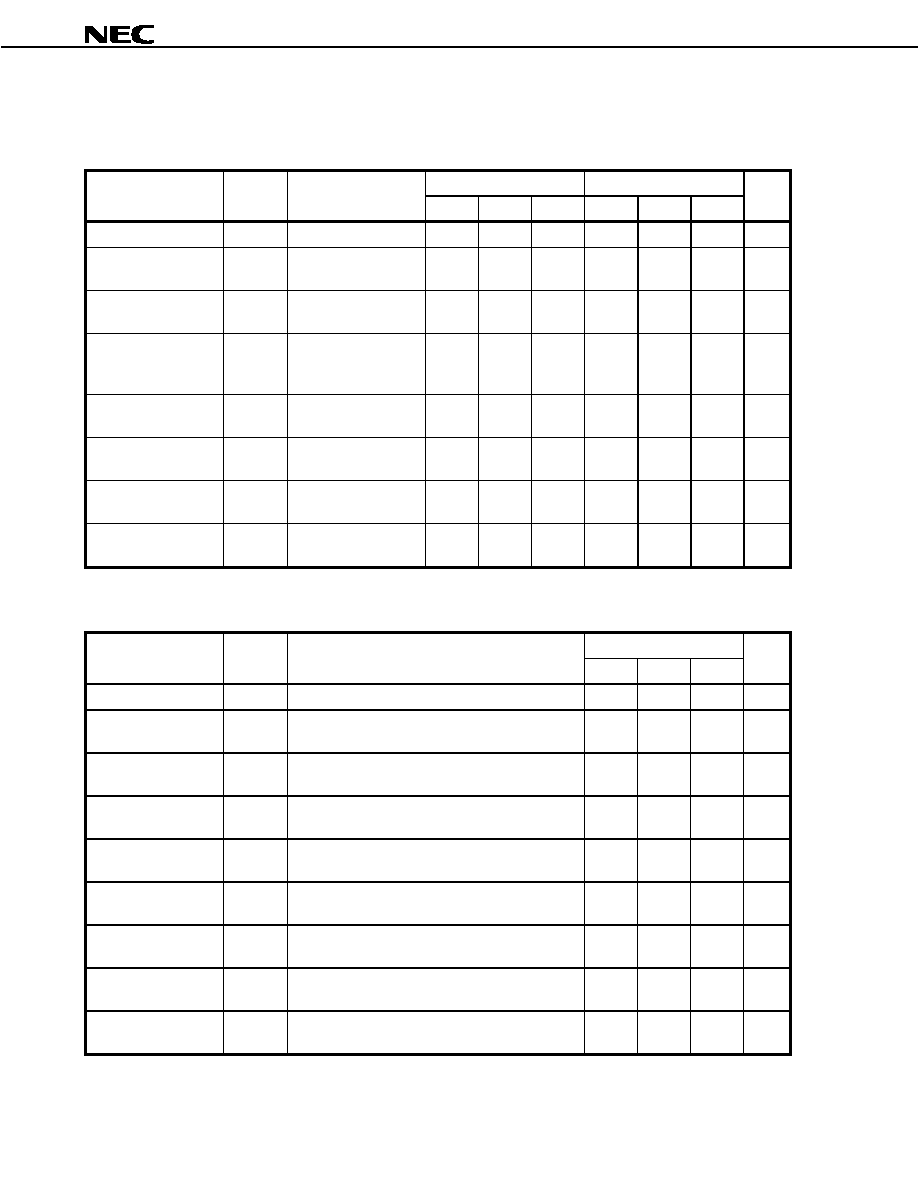
ELECTRICAL CHARACTERISTICS (T
A
= +25 ∞C, V
CC
= V
out
= 3.0 V, Z
L
= Z
S
= 50
)
µ
µ
µ
µ
PC2762TB,
µ
µ
µ
µ
PC2763TB
µ
PC2762TB
µ
PC2763TB
Parameter
Symbol
Test Conditions
MIN.
TYP.
MAX.
MIN.
TYP.
MAX.
Unit
Circuit Current
I
CC
No signal
-
26.5
35.0
-
27.0
35.0
mA
Power Gain
G
P
f = 0.9 GHz
f = 1.9 GHz
11
11.5
13
15.5
16
17.5
18
18
20
21
23
24
dB
Noise Figure
NF
f = 0.9 GHz
f = 1.9 GHz
-
-
6.5
7.0
8.0
9.0
-
-
5.5
5.5
7.0
7.5
dB
Upper Limit Operating
Frequency
f
u
3 dB down below
from gain at
f = 0.1 GHz
2.7
2.9
-
2.3
2.7
-
GHz
Isolation
ISL
f = 0.9 GHz
f = 1.9 GHz
22
20
27
25
-
-
25
24
30
29
-
-
dB
Input Return Loss
RL
in
f = 0.9 GHz
f = 1.9 GHz
6.0
5.5
9.0
8.5
-
-
8.0
8.0
11.0
11.0
-
-
dB
Output Return Loss
RL
out
f = 0.9 GHz
f = 1.9 GHz
8.0
9.0
11.0
12.0
-
-
5.0
6.0
7.0
9.0
-
-
dB
1 dB Gain Compres-
sion Output Level
P
O (1 dB)
f = 0.9 GHz
f = 1.9 GHz
+5.5
+4.5
+8.0
+7.0
-
-
+7.0
+4.0
+9.5
+6.5
-
-
dBm
µ
µ
µ
µ
PC2771TB
µ
PC2771TB
Parameter
Symbol
Test Conditions
MIN.
TYP.
MAX.
Unit
Circuit Current
I
CC
No signal
-
36.0
45.0
mA
Power Gain
G
P
f = 0.9 GHz
f = 1.5 GHz
19
18
21
21
24
24
dB
Noise Figure
NF
f = 0.9 GHz
f = 1.5 GHz
-
-
6.0
6.0
7.5
7.5
dB
Upper Limit Operating
Frequency
f
u
3 dB down below from gain at f = 0.1 GHz
1.8
2.2
-
GHz
Isolation
ISL
f = 0.9 GHz
f = 1.5 GHz
25
25
30
30
-
-
dB
Input Return Loss
RL
in
f = 0.9 GHz
f = 1.5 GHz
10
10
14
14
-
-
dB
Output Return Loss
RL
out
f = 0.9 GHz
f = 1.5 GHz
6.5
5.5
9.0
8.5
-
-
dB
1 dB Gain Compres-
Sion Output Level
P
O (1 dB)
f = 0.9 GHz
f = 1.5 GHz
+9.0
+7.0
+11.5
+9.5
-
-
dBm
Saturated Output
Power Level
P
O (sat)
f = 0.9 GHz
f = 1.5 GHz
-
-
+12.5
+11
-
-
dBm
Data Sheet P12710EJ2V0DS00
7
µ
µ
µ
µ
PC2762TB,
µ
µ
µ
µ
PC2763TB,
µ
µ
µ
µ
PC2771TB
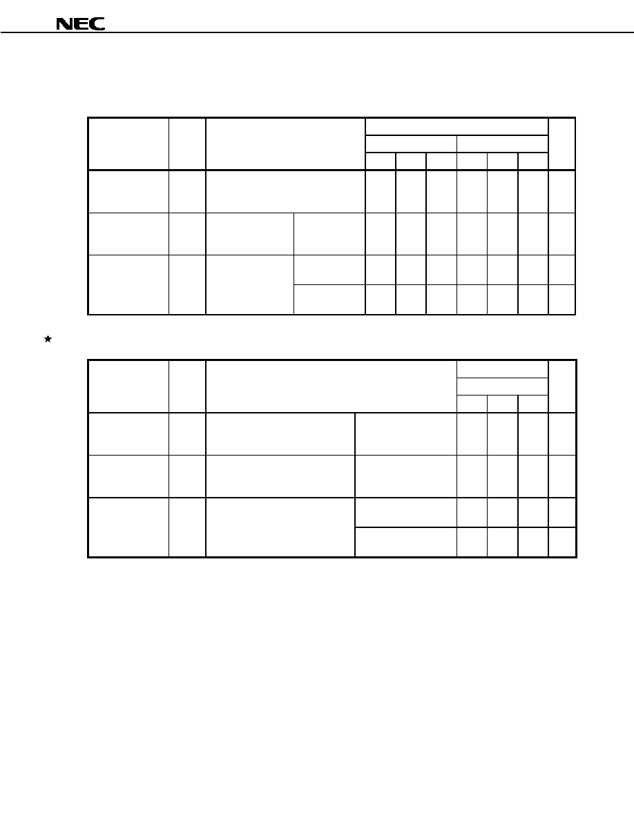
STANDARD CHARACTERISTICS FOR REFERENCE (T
A
= +25 ∞C, V
CC
= V
out
= 3.0 V, Z
L
= Z
S
= 50
)
µ
µ
µ
µ
PC2762TB,
µ
µ
µ
µ
PC2763TB
Reference
µ
PC2762TB
µ
PC2763TB
Parameter
Symbol
Test Conditions
MIN.
TYP.
MAX.
MIN.
TYP.
MAX.
Unit
Saturated
Output Power
Level
P
O (sat)
f = 0.9 GHz
f = 1.9 GHz
-
-
+9.0
+8.5
-
-
-
-
+11.0
+8.0
-
-
dBm
Adjacent channel
power
P
adj
f = 0.9 GHz
/4 QPSK wave
Note
P
O
= +4 dBm
f =
±
50 kHz
f =
±
100 kHz
-
-
-
64
-
64
-
-
-
-
-
61
-
62
-
-
dBc
Third order
intermodulation
IM
3
2 sine wave input.
Output of each tone
f
1
= 0.900 GHz
f
2
= 0.902 GHz
-
-
16
-
-
-
27
-
dBc
distortion
P
O
(each)
= +4 dBm
f
1
= 1.900 GHz
f
2
= 1.902 GHz
-
-
10
-
-
-
14
-
dBc
µ
µ
µ
µ
PC2771TB
Reference
µ
PC2771TB
Parameter
Symbol
Test Conditions
MIN.
TYP.
MAX.
Unit
Adjacent channel
power 1
P
adj
1
f = 0.9 GHz
/4 QPSK wave
Note
P
O
= +7 dBm
f =
±
50 kHz
f =
±
100 kHz
-
-
-
61
-
72
-
-
dBc
Adjacent channel
power 2
P
adj
2
f = 1.5 GHz
/4 QPSK wave
Note
P
O
= +7 dBm
f =
±
50 kHz
f =
±
100 kHz
-
-
-
59
-
71
-
-
dBc
Third order
intermodulation
IM
3
2 sine wave input.
Output of each tone
f
1
= 0.900 GHz
f
2
= 0.902 GHz
-
-
18
-
dBc
distortion
P
O
(each)
= +7 dBm
f
1
= 1.500 GHz
f
2
= 1.502 GHz
-
-
12
-
dBc
Note
/4 DQPSK modulated wave input, data rate 42 kbps, Filter roll off
= 0.5, PN 9
Data Sheet P12710EJ2V0DS00
8
µ
µ
µ
µ
PC2762TB,
µ
µ
µ
µ
PC2763TB,
µ
µ
µ
µ
PC2771TB
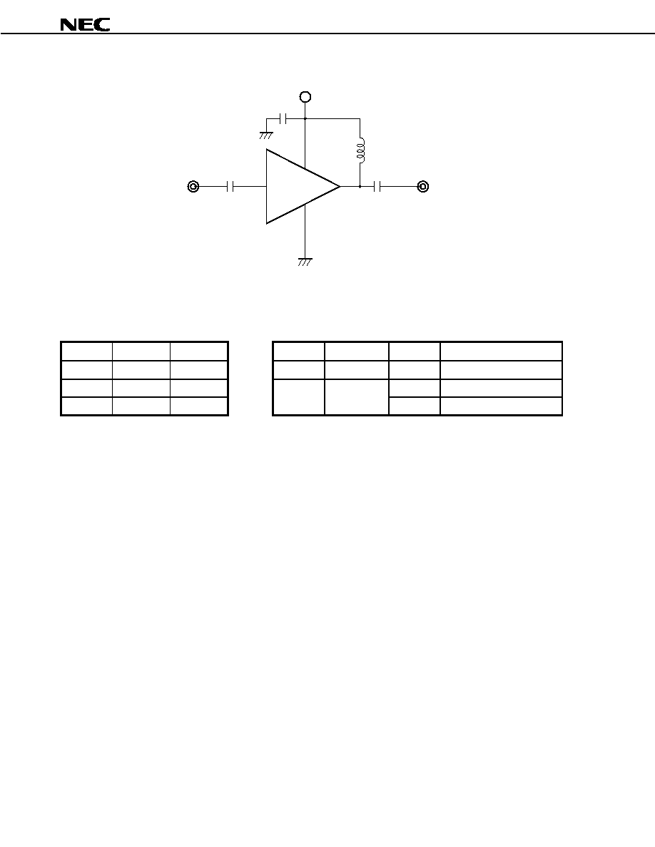
TEST CIRCUIT
V
CC
1 000 pF
1 000 pF
1 000 pF
C
1
C
2
L
4
6
1
2, 3, 5
50
50
OUT
IN
C
3
COMPONENTS OF TEST CIRCUIT
EXAMPLE OF ACTUAL APPLICATION COMPONENTS
FOR MEASURING ELECTRICAL
CHARACTERISTICS
Type
Value
Type
Value
Operating Frequency
C
1
, C
2
Bias Tee
1 000 pF
C
1
to C
3
Chip capacitor
1 000 pF
100 MHz or higher
C
3
Capacitor
1 000 pF
L
Chip inductor
100 nH
100 MHz or higher
L
Bias Tee
1 000 nH
10 nH
2.0 GHz or higher
INDUCTOR FOR THE OUTPUT PIN
The internal output transistor of this IC consumes 20 mA, to output medium power. To supply current for output
transistor, connect an inductor between the Vcc pin (pin 6) and output pin (pin 4). Select large value inductance, as
listed above.
The inductor has both DC and AC effects. In terms of DC, the inductor biases the output transistor with minimum
voltage drop to output enable high level. In terms of AC, the inductor make output-port-impedance higher to get
enough gain. In this case, large inductance and Q is suitable.
For above reason, select an inductance of 100
or over impedance in the operating frequency. The gain is a
peak in the operating frequency band, and suppressed at lower frequencies.
The recommendable inductance can be chosen from example of actual application components list as shown
above.
CAPACITORS FOR THE V
CC
, INPUT, AND OUTPUT PINS
Capacitors of 1 000 pF are recommendable as the bypass capacitor for the Vcc pin and the coupling capacitors
for the input and output pins.
The bypass capacitor connected to the Vcc pin is used to minimize ground impedance of Vcc pin. So, stable bias
can be supplied against Vcc fluctuation.
The coupling capacitors, connected to the input and output pins, are used to cut the DC and minimize RF serial
impedance. Their capacitance are therefore selected as lower impedance against a 50
load. The capacitors thus
perform as high pass filters, suppressing low frequencies to DC.
To obtain a flat gain from 100 MHz upwards, 1 000 pF capacitors are used in the test circuit. In the case of under
10 MHz operation, increase the value of coupling capacitor such as 10 000 pF. Because the coupling capacitors are
determined by equation, C = 1/(2
Rfc).
Data Sheet P12710EJ2V0DS00
9
µ
µ
µ
µ
PC2762TB,
µ
µ
µ
µ
PC2763TB,
µ
µ
µ
µ
PC2771TB
ILLUSTRATION OF THE TEST CIRCUIT ASSEMBLED ON EVALUATION BOARD
C1Z
3
2
1
4
5
6
Top View
IN
OUT
C
V
CC
AMP-2
C
C
L
Mounting direction
(Marking is an example for PC2762TB)
Notes
1.
2.
3.
4.
30
◊
30
◊
0.4 mm double sided copper clad polyimide board.
Back side: GND pattern
Solder plated on pattern
: Through holes
For more information on the use of this IC, refer to the following application note: USAGE AND APPLICATION OF
SILICON MEDIUM-POWER HIGH-FREQUENCY AMPLIFIER MMIC (P12152E).
COMPONENT LIST
Value
C
1 000 pF
L
Example: 10 nH
Data Sheet P12710EJ2V0DS00
10
µ
µ
µ
µ
PC2762TB,
µ
µ
µ
µ
PC2763TB,
µ
µ
µ
µ
PC2771TB
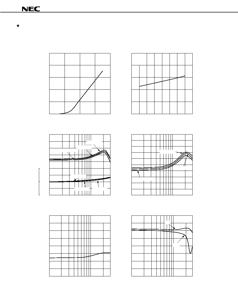
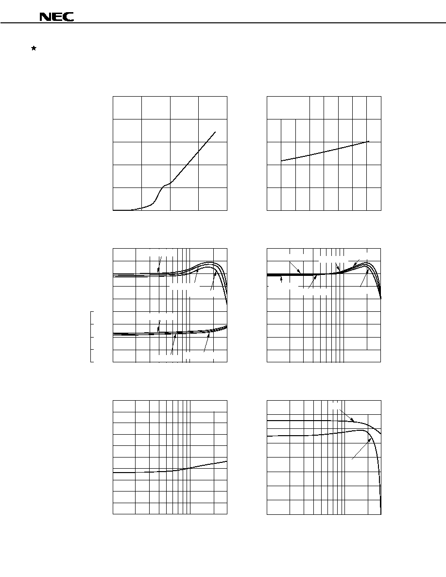
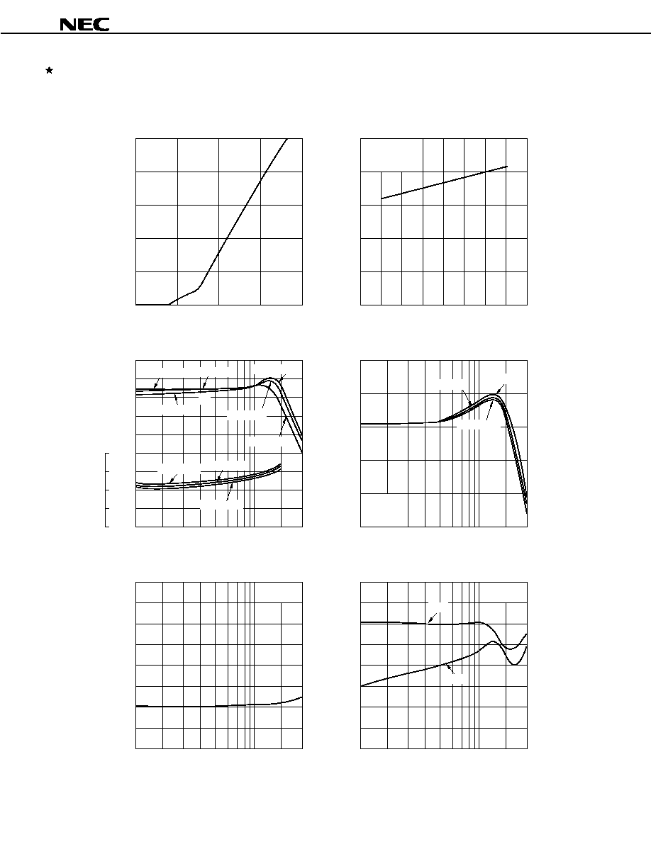
TYPICAL CHARACTERISTICS (Unless otherwise specified, T
A
= +25
∞
∞
∞
∞
C)
-
µ
PC2762TB
-
CIRCUIT CURRENT vs. SUPPLY VOLTAGE
CIRCUIT CURRENT vs. OPERATING
AMBIENT TEMPERATURE
Circuit Current I
CC
(mA)
Supply Voltage V
CC
(V)
Operating Ambient Temperature T
A
(
∞
C)
Frequency f (GHz)
ISOLATION vs. FREQUENCY
INPUT RETURN LOSS, OUTPUT RETURN
LOSS vs. FREQUENCY
Isolation ISL (dB)
Frequency f (GHz)
Frequency f (GHz)
Frequency f (GHz)
0
≠60
10
20
30
40
50
≠40 ≠20
0
+20
+40
+60
+80 +100
No signal
V
CC
= 3.0 V
NOISE FIGURE AND INSERTION POWER
GAIN vs. FREQUENCY
INSERTION POWER GAIN vs. FREQUENCY
Circuit Current I
CC
(mA)
Insertion Power Gain G
P
(dB)
No signal
0
10
20
30
40
50
1
2
3
4
≠40
≠30
≠20
0
≠10
1.0
3.0
0.1
0.3
V
CC
= 3.0 V
Input Return Loss RL
in
(dB)
Output Return Loss RL
out
(dB)
≠40
≠30
≠20
0
1.0
3.0
≠10
0.3
0.1
RL
in
RL
out
V
CC
= 3.0 V
Noise Figure NF (dB)
Insertion Power Gain G
P
(dB)
1.0
3.0
0.3
0.1
4
6
12
16
20
8
10
14
18
2
G
P
NF
V
CC
= 3.0 V
V
CC
= 3.3 V
V
CC
= 2.7 V
V
CC
= 3.3 V
V
CC
= 3.0 V
V
CC
= 2.7 V
4
6
8
10
2
8
0.1
10
12
14
16
18
T
A
= +85
∞
C
T
A
= ≠40
∞
C
T
A
= +25
∞
C
1.0
3.0
0.3
V
CC
= 3.0 V
Data Sheet P12710EJ2V0DS00
11
µ
µ
µ
µ
PC2762TB,
µ
µ
µ
µ
PC2763TB,
µ
µ
µ
µ
PC2771TB
-
µ
PC2762TB
-
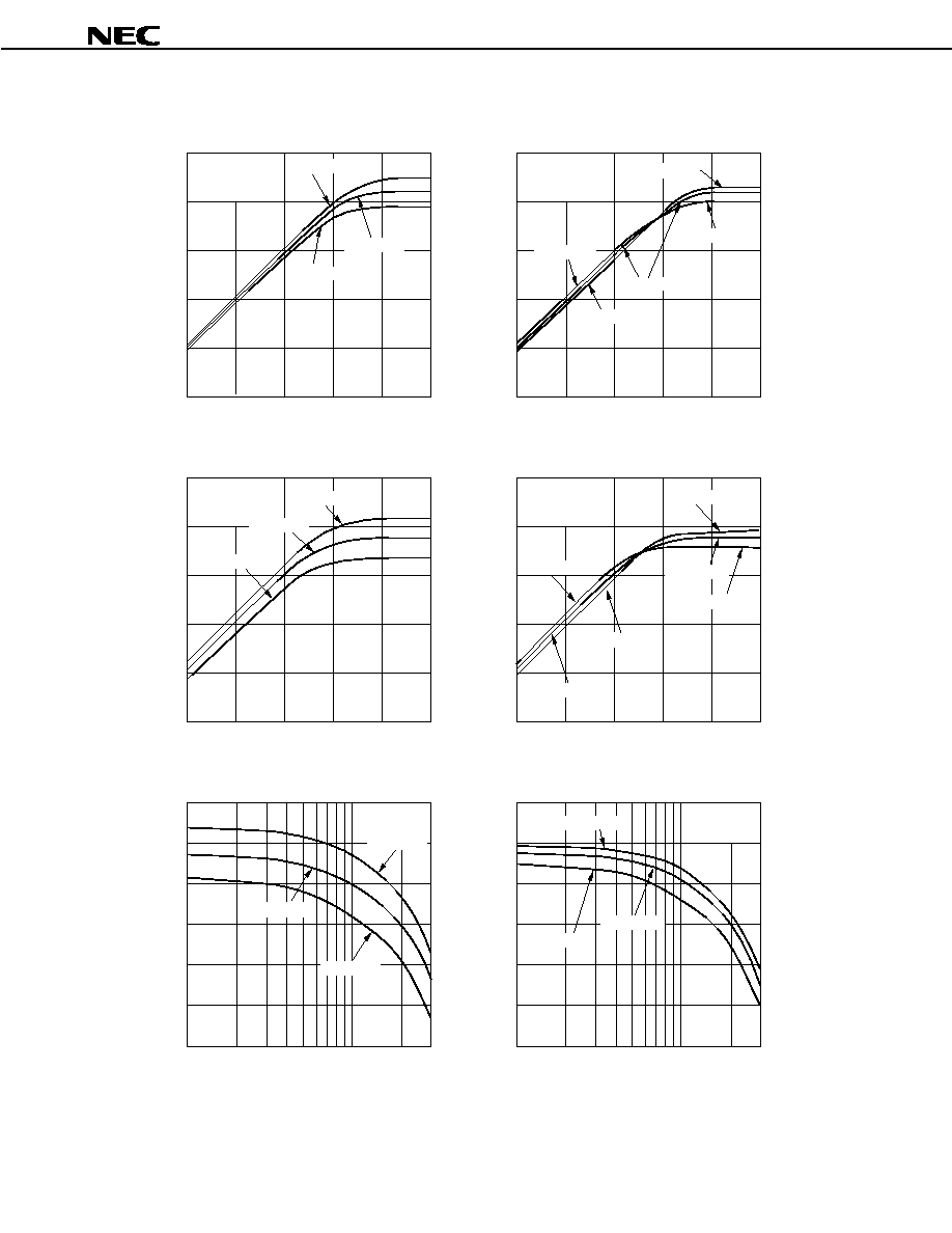
OUTPUT POWER vs. INPUT POWER
OUTPUT POWER vs. INPUT POWER
Output Power P
out
(dBm)
Output Power P
out
(dBm)
Output Power P
out
(dBm)
Input Power P
in
(dBm)
Input Power P
in
(dBm)
Input Power P
in
(dBm)
SATURATED OUTPUT POWER vs.
FREQUENCY
SATURATED OUTPUT POWER vs.
FREQUENCY
Saturated Output Power P
O (sat)
(dBm)
Saturated Output Power P
O (sat)
(dBm)
Frequency f (GHz)
Input Power P
in
(dBm)
≠10
≠20
≠15
+5
≠5
+15
0
+5
+10
≠10
≠5
0
≠10
≠20
≠5
0
+5
+10
+15
≠15
≠10
≠5
0
+5
OUTPUT POWER vs. INPUT POWER
OUTPUT POWER vs. INPUT POWER
Output Power P
out
(dBm)
f = 0.9 GHz
V
CC
= 3.0 V
V
CC
= 3.3 V
V
CC
= 2.7 V
≠10
≠20
≠15
+5
≠5
+15
T
A
= +85
∞
C
T
A
= +25
∞
C
T
A
= ≠40
∞
C
0
+5
+10
≠10
≠5
0
f = 0.9 GHz
V
CC
= 3.0 V
f = 1.9 GHz
Frequency f (GHz)
≠10
≠20
≠15
+5
≠5
+15
0
+5
+10
≠10
≠5
0
f = 1.9 GHz
V
CC
= 3.0 V
+3
0.1
+9
+11
+13
+5
+7
1.0
3.0
V
CC
= 3.3 V
V
CC
= 3.0 V
V
CC
= 2.7 V
0.3
+3
0.3
+5
+7
+9
+13
1.0
3.0
+11
P
in
= +3 dBm
P
in
= +3 dBm
0.1
T
A
= +85
∞
C
T
A
= +25
∞
C
T
A
= ≠40
∞
C
V
CC
= 3.0 V
V
CC
= 3.3 V
V
CC
= 2.7 V
T
A
= +85
∞
C
T
A
= +25
∞
C
T
A
= ≠40
∞
C
Data Sheet P12710EJ2V0DS00
12
µ
µ
µ
µ
PC2762TB,
µ
µ
µ
µ
PC2763TB,
µ
µ
µ
µ
PC2771TB
-
µ
PC2762TB
-
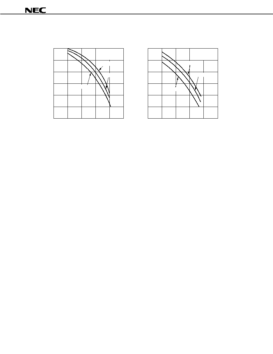
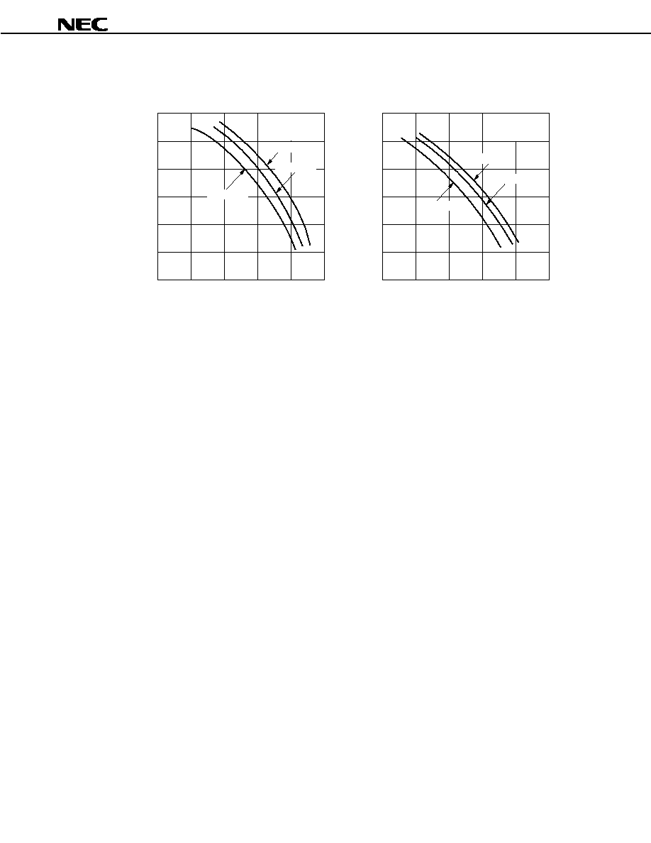
THIRD ORDER INTERMODULATION DISTORTION
vs. OUTPUT POWER OF EACH TONE
THIRD ORDER INTERMODULATION DISTORTION
vs. OUTPUT POWER OF EACH TONE
Third Order Intermodulation Distortion IM
3
(dBc)
Output Power of Each Tone P
O (each)
(dBm)
Output Power of Each Tone P
O (each)
(dBm)
0
≠15
≠10
≠20
≠30
≠50
≠60
≠10
≠5
0
+5
+10
Third Order Intermodulation Distortion IM
3
(dBc)
V
CC
= 3.3 V
V
CC
= 3.0 V
V
CC
= 2.7 V
≠40
0
≠15
≠10
≠20
≠30
≠50
≠60
≠10
≠5
0
+5
+10
≠40
V
CC
= 3.0 V
V
CC
= 2.7 V
f
1
= 0.900 GHz
f
2
= 0.902 GHz
f
1
= 1.900 GHz
f
2
= 1.902 GHz
V
CC
= 3.3 V

Data Sheet P12710EJ2V0DS00
13
µ
µ
µ
µ
PC2762TB,
µ
µ
µ
µ
PC2763TB,
µ
µ
µ
µ
PC2771TB
S-PARAMETER (T
A
= +25
∞
∞
∞
∞
C, V
CC
= V
out
= 3.0 V)
-
µ
PC2762TB
-
S
11
-FREQUENCY
0.1 G
2.0 G
3.0 G
S
22
-FREQUENCY
0.1G
3.0 G
1.0 G
2.0 G

Data Sheet P12710EJ2V0DS00
14
µ
µ
µ
µ
PC2762TB,
µ
µ
µ
µ
PC2763TB,
µ
µ
µ
µ
PC2771TB
TYPICAL S-PARAMETER VALUES (T
A
= +25
∞
∞
∞
∞
C)
µ
PC2762TB
V
CC
= V
out
= 3.0 V, I
CC
= 29 mA
FREQUENCY
S
11
S
21
S
12
S
22
K
MHz
MAG.
ANG.
MAG.
ANG.
MAG.
ANG.
MAG.
ANG.
100.0000
0.338
-
1.3
4.560
-
3.4
0.039
1.0
0.310
-
5.5
2.23
200.0000
0.346
-
2.0
4.581
-
7.6
0.039
2.7
0.311
-
9.5
2.20
300.0000
0.348
-
1.2
4.616
-
11.3
0.039
6.8
0.302
-
12.3
2.20
400.0000
0.340
-
1.9
4.661
-
15.8
0.040
8.1
0.296
-
16.2
2.18
500.0000
0.329
-
3.1
4.689
-
19.5
0.040
11.6
0.290
-
20.2
2.20
600.0000
0.324
-
6.2
4.726
-
23.6
0.041
13.7
0.292
-
24.1
2.12
700.0000
0.341
-
8.1
4.844
-
27.4
0.042
15.8
0.291
-
26.2
2.01
800.0000
0.359
-
7.6
4.927
-
31.5
0.043
18.1
0.292
-
28.3
1.90
900.0000
0.378
-
6.5
5.057
-
35.8
0.044
19.3
0.284
-
30.9
1.77
1000.0000
0.375
-
5.1
5.179
-
41.0
0.045
20.3
0.280
-
35.3
1.72
1100.0000
0.363
-
5.2
5.306
-
45.9
0.047
22.1
0.285
-
40.0
1.64
1200.0000
0.353
-
6.7
5.400
-
51.0
0.047
23.7
0.288
-
43.4
1.62
1300.0000
0.357
-
8.8
5.567
-
56.5
0.048
26.1
0.288
-
45.7
1.54
1400.0000
0.377
-
11.7
5.706
-
61.7
0.049
24.5
0.285
-
47.9
1.44
1500.0000
0.402
-
12.7
5.820
-
68.0
0.052
26.7
0.282
-
52.8
1.32
1600.0000
0.414
-
13.2
5.987
-
73.7
0.052
26.8
0.285
-
58.1
1.27
1700.0000
0.426
-
13.6
6.081
-
80.1
0.055
29.0
0.288
-
62.0
1.18
1800.0000
0.434
-
16.1
6.182
-
86.7
0.056
28.2
0.291
-
66.1
1.14
1900.0000
0.448
-
19.0
6.229
-
93.2
0.057
28.5
0.286
-
70.4
1.09
2000.0000
0.463
-
21.7
6.328
-
99.7
0.057
28.0
0.282
-
76.2
1.07
2100.0000
0.483
-
23.9
6.382
-
106.7
0.058
28.5
0.282
-
81.5
1.01
2200.0000
0.492
-
25.8
6.431
-
113.8
0.058
29.0
0.282
-
86.9
0.99
2300.0000
0.492
-
29.7
6.424
-
121.2
0.060
30.1
0.278
-
91.7
0.99
2400.0000
0.486
-
34.6
6.329
-
128.8
0.060
30.2
0.268
-
98.4
1.01
2500.0000
0.489
-
40.4
6.146
-
136.1
0.062
31.1
0.260
-
104.5
1.02
2600.0000
0.500
-
44.6
5.997
-
143.1
0.061
32.1
0.251
-
111.3
1.05
2700.0000
0.511
-
48.5
5.822
-
149.9
0.064
31.4
0.248
-
116.7
1.03
2800.0000
0.511
-
50.4
5.693
-
157.0
0.066
34.0
0.237
-
121.5
1.04
2900.0000
0.494
-
52.9
5.553
-
163.0
0.065
33.8
0.222
-
128.3
1.11
3000.0000
0.465
-
55.9
5.334
-
169.5
0.065
35.5
0.203
-
134.5
1.20
3100.0000
0.441
-
60.6
5.157
-
175.5
0.066
35.5
0.189
-
141.1
1.27
Data Sheet P12710EJ2V0DS00
15
µ
µ
µ
µ
PC2762TB,
µ
µ
µ
µ
PC2763TB,
µ
µ
µ
µ
PC2771TB
TYPICAL CHARACTERISTICS (Unless otherwise specified, T
A
= +25
∞
∞
∞
∞
C)
-
µ
PC2763TB
-
CIRCUIT CURRENT vs. SUPPLY VOLTAGE
CIRCUIT CURRENT vs. OPERATING
AMBIENT TEMPERATURE
Circuit Current I
CC
(mA)
Supply Voltage V
CC
(V)
Operating Ambient Temperature T
A
(
∞
C)
Frequency f (GHz)
ISOLATION vs. FREQUENCY
Isolation ISL (dB)
Frequency f (GHz)
Frequency f (GHz)
NOISE FIGURE AND INSERTION POWER
GAIN vs. FREQUENCY
INSERTION POWER GAIN vs. FREQUENCY
Circuit Current I
CC
(mA)
Insertion Power Gain G
P
(dB)
Frequency f (GHz)
INPUT RETURN LOSS, OUTPUT RETURN
LOSS vs. FREQUENCY
0
10
20
30
40
1
2
3
4
10
≠60
30
50
≠40
≠20
0
5
≠50
0.1
≠30
≠20
≠10
0
≠40
≠40
0.1
≠30
≠20
≠10
0
0.3
1.0
3.0
RL
in
3
7
50
0
20
40
Noise Figure NF (dB)
Insertion Power Gain G
P
(dB)
Input Return Loss RL
in
(dB)
Output Return Loss RL
out
(dB)
0.3
1.0
3.0
RLo
6
0.1
14
16
22
24
8
10
12
18
20
0.3
1.0
3.0
VCC = 3.3
NF
G
P
TA = ≠40
∞
C
TA = +85
∞
C
VCC = 2.7
VCC = 3.0
VCC = 3.3
6
0.1
14
16
22
24
8
10
12
18
20
0.3
1.0
3.0
VCC = 2.7
VCC = 3.0
TA = +85
∞
C
TA = +25
∞
C
TA = ≠40
∞
C
TA = +25
∞
C
V
CC
= 3.0 V
0
10
20
30
40
1
2
3
4
10
≠60
30
50
≠40
≠20
+20
+40
+100
0
+80
+60
5
≠50
0.1
≠30
≠20
≠10
0
≠40
≠40
0.1
≠30
≠20
≠10
0
0.3
1.0
3.0
3
7
50
No signal
No signal
V
CC
= 3.0 V
0
20
40
0.3
1.0
3.0
RL
out
V
CC
= 3.0 V
6
4
6
0.1
14
16
22
24
8
10
12
18
20
0.3
1.0
3.0
V
CC
= 3.3 V
NF
T
A
= ≠40
∞
C
T
A
= +85
∞
C
V
CC
= 3.0 V
V
CC
= 2.7 V
V
CC
= 3.0 V
V
CC
= 3.3 V
6
0.1
14
16
22
24
8
10
12
18
20
0.3
1.0
3.0
V
CC
= 2.7 V
V
CC
= 3.0 V
T
A
= +85
∞
C
T
A
= +25
∞
C
T
A
= ≠40
∞
C
T
A
= +25
∞
C
Data Sheet P12710EJ2V0DS00
16
µ
µ
µ
µ
PC2762TB,
µ
µ
µ
µ
PC2763TB,
µ
µ
µ
µ
PC2771TB
-
µ
PC2763TB
-
OUTPUT POWER vs. INPUT POWER
OUTPUT POWER vs. INPUT POWER
Output Power P
out
(dBm)
Output Power P
out
(dBm)
Input Power P
in
(dBm)
Input Power P
in
(dBm)
Input Power P
in
(dBm)
SATURATED OUTPUT POWER vs.
FREQUENCY
SATURATED OUTPUT POWER vs.
FREQUENCY
Saturated Output Power P
O (sat)
(dBm)
Frequency f (GHz)
Input Power P
in
(dBm)
OUTPUT POWER vs. INPUT POWER
OUTPUT POWER vs. INPUT POWER
Output Power P
out
(dBm)
Output Power P
out
(dBm)
Saturated Output Power P
O (sat)
(dBm)
Frequency f (GHz)
≠5
+3
0.1
0
+5
+10
+15
≠5
0
+5
+10
+15
+9
+11
+13
+15
≠10
≠25
0
+5
+10
+15
+5
+10
+15
≠20
≠15
≠10
≠5
0
≠5
T
A
= +85
∞
C
T
A
= +25
∞
C
T
A
= ≠40
∞
C
T
A
= +85
∞
C
T
A
= ≠40
∞
C
V
CC
= 3.3 V
V
CC
= 3.0 V
V
CC
= 2.7 V
+5
+7
1.0
3.0
T
A
= +25
∞
C
T
A
= +85
∞
C
T
A
= ≠40
∞
C
T
A
= ≠40
∞
C
T
A
= +85
∞
C
T
A
= +25
∞
C
+3
0.1
+5
+9
+11
+13
+15
1.0
3.0
+7
≠25
≠20
≠15
≠10
≠5
0
f = 0.9 GHz
V
CC
= 3.0 V
f = 0.9 GHz
f = 1.9 GHz
f = 1.9 GHz
V
CC
= 3.0 V
≠25
≠20
≠15
≠10
≠5
0
≠10
≠25
≠20
≠15
≠10
≠5
0
0.3
0.3
P
in
= ≠3 dBm
P
in
= ≠3 dBm
V
CC
= 3.3 V
V
CC
= 3.0 V
V
CC
= 2.7 V
≠10
0
≠5
≠10
V
CC
= 3.3 V
V
CC
= 3.0 V
V
CC
= 2.7 V
T
A
= ≠40
∞
C
T
A
= +25
∞
C
T
A
= +85
∞
C
Data Sheet P12710EJ2V0DS00
17
µ
µ
µ
µ
PC2762TB,
µ
µ
µ
µ
PC2763TB,
µ
µ
µ
µ
PC2771TB
-
µ
PC2763TB
-
Third Order Intermodulation Distortion IM
3
(dBc)
Output Power of Each Tone P
O (each)
(dBm)
Output Power of Each Tone P
O (each)
(dBm)
Third Order Intermodulation Distortion IM
3
(dBc)
THIRD ORDER INTERMODULATION DISTORTION vs.
OUTPUT POWER OF EACH TONE
THIRD ORDER INTERMODULATION DISTORTION vs.
OUTPUT POWER OF EACH TONE
0
≠15
≠10
≠20
≠50
≠60
≠10
≠5
0
+5
+10
V
CC
= 3.3 V
V
CC
= 2.7 V
0
≠20
≠30
≠50
≠60
≠10
≠30
≠40
V
CC
= 3.0 V
V
CC
= 3.3 V
V
CC
= 2.7 V
V
CC
= 3.0 V
≠40
≠15
≠10
≠5
0
+5
+10
f
1
= 0.900 GHz
f
2
= 0.902 GHz
f
1
= 1.900 GHz
f
2
= 1.902 GHz

Data Sheet P12710EJ2V0DS00
18
µ
µ
µ
µ
PC2762TB,
µ
µ
µ
µ
PC2763TB,
µ
µ
µ
µ
PC2771TB
S-PARAMETER (T
A
= +25
∞
∞
∞
∞
C, V
CC
= V
out
= 3.0 V)
-
µ
PC2763TB
-
S
11
-FREQUENCY
0.1 G
2.0 G
1.0 G
3.0 G
S
22
-FREQUENCY
0.1 G
1.0 G
2.0 G
3.0 G

Data Sheet P12710EJ2V0DS00
19
µ
µ
µ
µ
PC2762TB,
µ
µ
µ
µ
PC2763TB,
µ
µ
µ
µ
PC2771TB
TYPICAL S-PARAMETER VALUES (T
A
= +25
∞
∞
∞
∞
C)
µ
PC2763TB
V
CC
= V
out
= 3.0 V, I
CC
= 28 mA
FREQUENCY
S
11
S
21
S
12
S
22
K
MHz
MAG.
ANG.
MAG.
ANG.
MAG.
ANG.
MAG.
ANG.
100.0000
0.231
-
1.4
10.210
-
3.8
0.023
2.4
0.406
-
4.1
1.68
200.0000
0.242
-
0.2
10.305
-
8.5
0.023
7.8
0.412
-
7.5
1.66
300.0000
0.250
2.7
10.464
-
12.9
0.024
9.3
0.407
-
9.9
1.58
400.0000
0.245
2.8
10.655
-
18.2
0.024
13.4
0.407
-
13.9
1.55
500.0000
0.242
2.0
10.863
-
22.8
0.026
16.1
0.405
-
17.6
1.44
600.0000
0.241
-
2.2
11.093
-
28.1
0.027
19.9
0.414
-
21.6
1.37
700.0000
0.263
-
5.3
11.544
-
33.2
0.028
22.3
0.419
-
24.6
1.25
800.0000
0.291
-
5.6
11.843
-
39.0
0.029
22.5
0.424
-
27.7
1.16
900.0000
0.316
-
5.1
12.291
-
45.1
0.029
23.9
0.424
-
31.9
1.09
1000.0000
0.322
-
4.0
12.676
-
52.4
0.030
25.6
0.425
-
37.1
1.02
1100.0000
0.318
-
5.4
13.066
-
59.8
0.031
24.1
0.438
-
42.5
0.96
1200.0000
0.309
-
9.0
13.311
-
67.3
0.031
27.0
0.442
-
47.8
0.96
1300.0000
0.322
-
14.2
13.661
-
75.8
0.033
28.8
0.441
-
51.2
0.90
1400.0000
0.344
-
20.6
13.845
-
83.9
0.033
28.5
0.434
-
56.0
0.87
1500.0000
0.371
-
23.7
13.824
-
93.0
0.035
30.1
0.435
-
62.2
0.82
1600.0000
0.380
-
27.5
13.890
-
101.5
0.035
28.1
0.439
-
68.9
0.80
1700.0000
0.388
-
30.6
13.634
-
110.5
0.036
29.2
0.439
-
74.6
0.78
1800.0000
0.378
-
36.4
13.236
-
119.6
0.035
29.9
0.428
-
81.3
0.84
1900.0000
0.378
-
42.1
12.724
-
127.9
0.035
30.9
0.411
-
87.0
0.89
2000.0000
0.375
-
46.6
12.290
-
136.1
0.035
32.9
0.393
-
93.4
0.94
2100.0000
0.369
-
50.5
11.707
-
144.0
0.035
33.0
0.385
-
99.6
0.99
2200.0000
0.351
-
53.8
11.130
-
151.7
0.036
35.7
0.373
-
104.9
1.06
2300.0000
0.331
-
59.8
10.524
-
159.1
0.036
36.8
0.359
-
110.3
1.13
2400.0000
0.306
-
66.4
9.824
-
165.9
0.034
38.7
0.336
-
117.5
1.31
2500.0000
0.300
-
73.1
9.152
-
172.3
0.035
40.1
0.321
-
123.3
1.41
2600.0000
0.294
-
75.8
8.583
-
178.2
0.034
43.8
0.306
-
129.4
1.55
2700.0000
0.290
-
77.1
8.029
176.2
0.035
46.3
0.299
-
133.9
1.58
2800.0000
0.270
-
77.7
7.610
170.6
0.037
47.7
0.288
-
138.6
1.63
2900.0000
0.248
-
78.7
7.240
166.1
0.039
51.1
0.270
-
143.6
1.67
3000.0000
0.219
-
82.3
6.827
161.2
0.039
53.6
0.253
-
150.1
1.79
3100.0000
0.198
-
88.7
6.516
156.9
0.040
55.1
0.244
-
156.2
1.88
Data Sheet P12710EJ2V0DS00
20
µ
µ
µ
µ
PC2762TB,
µ
µ
µ
µ
PC2763TB,
µ
µ
µ
µ
PC2771TB
TYPICAL CHARACTERISTICS (Unless otherwise specified, T
A
= +25
∞
∞
∞
∞
C)
-
µ
PC2771TB
-
CIRCUIT CURRENT vs. OPERATING
AMBIENT TEMPERATURE
Circuit Current I
CC
(mA)
Supply Voltage V
CC
(V)
Operating Ambient Temperature T
A
(
∞
C)
Frequency f (GHz)
ISOLATION vs. FREQUENCY
Isolation ISL (dB)
Frequency f (GHz)
Frequency f (GHz)
NOISE FIGURE AND INSERTION POWER
GAIN vs. FREQUENCY
INSERTION POWER GAIN vs. FREQUENCY
Circuit Current I
CC
(mA)
Insertion Power Gain G
P
(dB)
Frequency f (GHz)
INPUT RETURN LOSS, OUTPUT RETURN
LOSS vs. FREQUENCY
CIRCUIT CURRENT vs. SUPPLY VOLTAGE
14
0.1
24
0.1
22
20
18
16
0.3
1.0
3.0
22
24
0.3
1.0
3.0
Insertion Power Gain G
P
(dB)
50
50
20
0
1
2
3
40
30
20
10
0
+100
18
0.1
0
0.1
0.3
1.0
3.0
≠10
≠20
≠30
≠40
1.0
3.0
4
10
30
40
0
≠60 ≠40
≠20
+20
+40 +60 +80
14
No signal
No signal
V
CC
= 3.0 V
V
CC
= 2.7 V
V
CC
= 3.0 V
V
CC
= 3.3 V
V
CC
= 2.7 V
V
CC
= 3.0 V
V
CC
= 3.3 V
20
16
T
A
= ≠40
∞
C
T
A
= +25
∞
C
T
A
= +85
∞
C
0.3
Input Return Loss RL
in
(dB)
Outpur Return Loss RL
out
(dB)
RL
out
RL
in
V
CC
= 3.0 V
V
CC
= 2.7 V
V
CC
= 3.3 V
12
10
8
6
5
6
7
4
3
Noise Figure NF (dB)
G
P
NF
V
CC
= 3.0 V
0
≠10
≠20
≠30
≠40
V
CC
= 3.0 V
V
CC
= 3.0 V
Data Sheet P12710EJ2V0DS00
21
µ
µ
µ
µ
PC2762TB,
µ
µ
µ
µ
PC2763TB,
µ
µ
µ
µ
PC2771TB
-
µ
PC2771TB
-
OUTPUT POWER vs. INPUT POWER
Output Power P
out
(dBm)
Output Power P
out
(dBm)
Input Power P
in
(dBm)
Input Power P
in
(dBm)
Input Power P
in
(dBm)
OUTPUT POWER vs. INPUT POWER
Output Power P
out
(dBm)
Input Power P
in
(dBm)
Input Power P
in
(dBm)
OUTPUT POWER vs. INPUT POWER
OUTPUT POWER vs. INPUT POWER
Output Power P
out
(dBm)
Output Power P
out
(dBm)
Output Power P
out
(dBm)
Input Power P
in
(dBm)
OUTPUT POWER vs. INPUT POWER
OUTPUT POWER vs. INPUT POWER
0
≠5
≠10
+15
0
≠20
≠15
≠10
0
≠5
+15
0
0
≠5
+5
+10
+15
+5
+10
+15
+5
+10
+15
+5
+10
V
CC
= 3.3 V
+10
+5
≠5
≠10
≠25
≠5
f = 0.9 GHz
V
CC
= 3.0 V
V
CC
= 2.7 V
≠20
≠15
≠10
0
≠25
≠5
f = 0.9 GHz
V
CC
= 3.0 V
T
A
= +85
∞
C
T
A
= +25
∞
C
T
A
= ≠40
∞
C
≠20
≠15
≠10
0
≠25
≠5
f = 1.5 GHz
0
≠5
≠20
≠15
≠10
0
≠25
≠5
f = 1.5 GHz
V
CC
= 3.0 V
T
A
= +85
∞
C
T
A
= ≠40
∞
C
T
A
= +25
∞
C
T
A
= +85
∞
C
T
A
= ≠40
∞
C
T
A
= +25
∞
C
T
A
= ≠40
∞
C
T
A
= +85
∞
C
T
A
= +25
∞
C
f = 1.9 GHz
f = 1.9 GHz
V
CC
= 3.0 V
≠20
≠15
≠10
0
≠25
≠5
V
CC
= 2.7 V
V
CC
= 3.0 V
V
CC
= 3.3 V
+15
+10
≠5
≠10
≠20
≠15
≠10
0
≠25
≠5
+5
0
T
A
= ≠40 ∞C
T
A
= +85 ∞C
T
A
= +25 ∞C
V
CC
= 2.7 V
V
CC
= 3.0 V
V
CC
= 3.3 V
Data Sheet P12710EJ2V0DS00
22
µ
µ
µ
µ
PC2762TB,
µ
µ
µ
µ
PC2763TB,
µ
µ
µ
µ
PC2771TB
-
µ
PC2771TB
-
Saturated Output Power P
O (sat)
(dBm)
Third Order Intermodulation Distortion IM
3
(dBc)
Frequency f (GHz)
Frequency f (GHz)
Output Power of Each Tone P
O (each)
(dBm)
Output Power of Each Tone P
O (each)
(dBm)
THIRD ORDER INTERMODULATION DISTORTION vs.
OUTPUT POWER OF EACH TONE
THIRD ORDER INTERMODULATION DISTORTION vs.
OUTPUT POWER OF EACH TONE
Saturated Output Power P
O (sat)
(dBm)
Third Order Intermodulation Distortion IM
3
(dBc)
SATURATED OUTPUT POWER vs.
FREQUENCY
SATURATED OUTPUT POWER vs.
FREQUENCY
+17
+9
1.0
≠60
≠30
≠5
+10
+7
+13
+15
≠50
≠40
≠20
≠10
+11
+5
0.1
V
CC
= 3.0 V
V
CC
= 2.7 V
P
in
= ≠3 dBm
+17
+9
+7
+13
+15
+11
+5
P
in
= ≠3 dBm
T
A
= +85
∞
C
T
A
= +25
∞
C
T
A
= ≠40
∞
C
0
0
≠10
≠60
≠30
≠15
+10
≠50
≠40
≠20
≠10
0
≠5
0
≠10
f
1
= 0.900 GHz
f
2
= 0.902 GHz
f
1
= 1.500 GHz
f
2
= 1.502 GHz
V
CC
= 3.3 V
V
CC
= 3.0 V
V
CC
= 2.7 V
+5
≠15
+5
0.3
3.0
1.0
0.1
0.3
3.0
V
CC
= 3.3 V
V
CC
= 3.0 V
V
CC
= 2.7 V
V
CC
= 3.3 V
Data Sheet P12710EJ2V0DS00
23
µ
µ
µ
µ
PC2762TB,
µ
µ
µ
µ
PC2763TB,
µ
µ
µ
µ
PC2771TB
S-PARAMETER (T
A
= +25
∞
∞
∞
∞
C, V
CC
= V
out
= 3.0 V)
-
µ
PC2771TB
-
S
11
-FREQUENCY
0.1 G
3.0 G
2.0 G
S
22
-FREQUENCY
0.1G
3.0 G
2.0 G

Data Sheet P12710EJ2V0DS00
24
µ
µ
µ
µ
PC2762TB,
µ
µ
µ
µ
PC2763TB,
µ
µ
µ
µ
PC2771TB
TYPICAL S-PARAMETER VALUES (T
A
= +25
∞
∞
∞
∞
C)
µ
PC2771TB
V
CC
= V
out
= 3.0 V, I
CC
= 35 mA
FREQUENCY
S
11
S
21
S
12
S
22
K
MHz
MAG.
ANG.
MAG.
ANG.
MAG.
ANG.
MAG.
ANG.
100.0000
0.045
19.7
10.570
-
4.7
0.028
0.8
0.327
-
6.2
1.65
200.0000
0.057
37.0
10.638
-
9.5
0.028
5.0
0.325
-
11.5
1.63
300.0000
0.075
41.3
10.775
-
14.1
0.029
8.6
0.323
-
16.2
1.58
400.0000
0.090
43.3
11.004
-
19.4
0.030
11.1
0.326
-
20.9
1.49
500.0000
0.105
42.2
11.275
-
24.4
0.030
14.9
0.331
-
26.4
1.45
600.0000
0.118
40.2
11.586
-
30.0
0.031
15.8
0.342
-
32.0
1.37
700.0000
0.138
34.9
12.041
-
35.9
0.031
19.8
0.350
-
37.3
1.29
800.0000
0.163
32.5
12.367
-
42.1
0.032
20.1
0.359
-
42.8
1.20
900.0000
0.186
29.4
12.844
-
48.8
0.032
23.2
0.361
-
49.4
1.15
1000.0000
0.202
26.3
13.300
-
56.6
0.032
23.9
0.371
-
56.1
1.11
1100.0000
0.219
21.7
13.771
-
64.6
0.033
24.9
0.389
-
62.5
1.03
1200.0000
0.233
15.4
14.082
-
73.5
0.033
26.6
0.400
-
69.3
0.99
1300.0000
0.252
8.4
14.365
-
83.2
0.036
28.8
0.405
-
75.4
0.92
1400.0000
0.267
-
0.1
14.336
-
92.6
0.036
30.0
0.402
-
83.6
0.91
1500.0000
0.285
-
6.8
14.142
-
102.4
0.036
32.0
0.406
-
91.6
0.90
1600.0000
0.293
-
13.9
13.929
-
112.0
0.037
31.6
0.413
-
99.3
0.89
1700.0000
0.304
-
20.9
13.428
-
121.6
0.039
32.5
0.414
-
105.8
0.88
1800.0000
0.290
-
28.1
12.722
-
131.0
0.038
34.7
0.401
-
113.7
0.96
1900.0000
0.285
-
35.3
11.966
-
139.6
0.038
36.1
0.387
-
120.8
1.03
2000.0000
0.273
-
41.8
11.232
-
147.5
0.038
37.4
0.378
-
127.6
1.09
2100.0000
0.267
-
47.4
10.500
-
154.8
0.039
39.1
0.366
-
133.1
1.14
2200.0000
0.254
-
51.6
9.815
-
161.7
0.040
41.4
0.356
-
138.0
1.20
2300.0000
0.237
-
57.1
9.168
-
168.0
0.041
43.7
0.342
-
142.8
1.28
2400.0000
0.221
-
61.1
8.570
-
173.7
0.041
48.3
0.325
-
148.3
1.37
2500.0000
0.212
-
68.8
7.967
-
179.7
0.042
48.3
0.322
-
152.6
1.44
2600.0000
0.208
-
72.2
7.507
174.9
0.043
50.8
0.314
-
156.7
1.49
2700.0000
0.202
-
74.1
7.004
170.0
0.045
53.7
0.309
-
160.1
1.53
2800.0000
0.190
-
76.3
6.667
164.7
0.047
54.2
0.303
-
164.0
1.56
2900.0000
0.178
-
76.7
6.336
160.7
0.051
57.7
0.292
-
167.8
1.55
3000.0000
0.154
-
82.3
6.003
155.6
0.051
56.5
0.287
-
172.8
1.62
3100.0000
0.147
-
88.0
5.772
151.3
0.054
59.3
0.279
-
176.4
1.61

Data Sheet P12710EJ2V0DS00
25
µ
µ
µ
µ
PC2762TB,
µ
µ
µ
µ
PC2763TB,
µ
µ
µ
µ
PC2771TB
PACKAGE DIMENSIONS
6 pin super minimold (Unit: mm)
1.25
±
0.1
2.1
±
0.1
0.65
0.65
1.3
2.0
±
0.2
0.1 MIN.
0.7
0.9
±
0.1
0 to 0.1
0.2
+0.1
≠0
0.15
+0.1
≠0
Data Sheet P12710EJ2V0DS00
26
µ
µ
µ
µ
PC2762TB,
µ
µ
µ
µ
PC2763TB,
µ
µ
µ
µ
PC2771TB
NOTES ON CORRECT USE
(1) Observe precautions for handling because of electro-static sensitive devices.
(2) Form a ground pattern as wide as possible to minimize ground impedance (to prevent undesired oscillation).
All the ground pins must be connected together with wide ground pattern to decrease impedance difference.
(3) The bypass capacitor should be attached to the V
CC
pin.
(4) The inductor must be attached between V
CC
and output pins. The inductance value should be determined in
accordance with desired frequency.
(5) The DC cut capacitor must be attached to input pin.
RECOMMENDED SOLDERING CONDITIONS
This product should be soldered under the following recommended conditions. For soldering methods and
conditions other than those recommended below, contact your NEC sales representative.
Soldering Method
Soldering Conditions
Recommended Condition Symbol
Infrared Reflow
Package peak temperature: 235 ∞C or below
Time: 30 seconds or less (at 210 ∞C)
Count: 3, Exposure limit: None
Note
IR35-00-3
VPS
Package peak temperature: 215 ∞C or below
Time: 40 seconds or less (at 200 ∞C)
Count: 3, Exposure limit: None
Note
VP15-00-3
Wave Soldering
Soldering bath temperature: 260 ∞C or below
Time: 10 seconds or less
Count: 1, Exposure limit: None
Note
WS60-00-1
Partial Heating
Pin temperature: 300 ∞C
Time: 3 seconds or less (per side of device)
Exposure limit: None
Note
≠
Note After opening the dry pack, keep it in a place below 25 ∞C and 65 % RH for the allowable storage period.
Caution Do not use different soldering methods together (except for partial heating).
For details of recommended soldering conditions for surface mounting, refer to information document
SEMICONDUCTOR DEVICE MOUNTING TECHNOLOGY MANUAL (C10535E).

Data Sheet P12710EJ2V0DS00
27
µ
µ
µ
µ
PC2762TB,
µ
µ
µ
µ
PC2763TB,
µ
µ
µ
µ
PC2771TB
[MEMO]
µ
µ
µ
µ
PC2762TB,
µ
µ
µ
µ
PC2763TB,
µ
µ
µ
µ
PC2771TB
ATTENTION
OBSERVE PRECAUTIONS
FOR HANDLING
ELECTROSTATIC
SENSITIVE
DEVICES
NESAT (NEC Silicon Advanced Technology) is a trademark of NEC Corporation.
∑
The information in this document is subject to change without notice. Before using this document, please
confirm that this is the latest version.
∑
No part of this document may be copied or reproduced in any form or by any means without the prior written
consent of NEC Corporation. NEC Corporation assumes no responsibility for any errors which may appear in
this document.
∑
NEC Corporation does not assume any liability for infringement of patents, copyrights or other intellectual property
rights of third parties by or arising from use of a device described herein or any other liability arising from use
of such device. No license, either express, implied or otherwise, is granted under any patents, copyrights or other
intellectual property rights of NEC Corporation or others.
∑
Descriptions of circuits, software, and other related information in this document are provided for illustrative
purposes in semiconductor product operation and application examples. The incorporation of these circuits,
software, and information in the design of the customer's equipment shall be done under the full responsibility
of the customer. NEC Corporation assumes no responsibility for any losses incurred by the customer or third
parties arising from the use of these circuits, software, and information.
∑
While NEC Corporation has been making continuous effort to enhance the reliability of its semiconductor devices,
the possibility of defects cannot be eliminated entirely. To minimize risks of damage or injury to persons or
property arising from a defect in an NEC semiconductor device, customers must incorporate sufficient safety
measures in its design, such as redundancy, fire-containment, and anti-failure features.
∑
NEC devices are classified into the following three quality grades:
"Standard", "Special", and "Specific". The Specific quality grade applies only to devices developed based on a
customer designated "quality assurance program" for a specific application. The recommended applications of
a device depend on its quality grade, as indicated below. Customers must check the quality grade of each device
before using it in a particular application.
Standard: Computers, office equipment, communications equipment, test and measurement equipment,
audio and visual equipment, home electronic appliances, machine tools, personal electronic
equipment and industrial robots
Special: Transportation equipment (automobiles, trains, ships, etc.), traffic control systems, anti-disaster
systems, anti-crime systems, safety equipment and medical equipment (not specifically designed
for life support)
Specific: Aircraft, aerospace equipment, submersible repeaters, nuclear reactor control systems, life
support systems or medical equipment for life support, etc.
The quality grade of NEC devices is "Standard" unless otherwise specified in NEC's Data Sheets or Data Books.
If customers intend to use NEC devices for applications other than those specified for Standard quality grade,
they should contact an NEC sales representative in advance.
M7 98. 8