 | –≠–ª–µ–∫—Ç—Ä–æ–Ω–Ω—ã–π –∫–æ–º–ø–æ–Ω–µ–Ω—Ç: UPC2776T | –°–∫–∞—á–∞—Ç—å:  PDF PDF  ZIP ZIP |
Caution: Electro-static sensitive devices
BIPOLAR ANALOG INTEGRATED CIRCUITS
µ
µ
µ
µ
PC2776TB
5 V, SUPER MINIMOLD SILICON MMIC
MEDIUM OUTPUT POWER AMPLIFIER
1997
©
Document No. P12680EJ2V0DS00 (2nd edition)
Date Published February 1998 N CP(K)
Printed in Japan
DATA SHEET
DESCRIPTION
The
µ
PC2776TB is a silicon monolithic integrated circuits designed as wideband amplifier. This amplifier has
impedance near 50
in HF band, so this IC suits to the system of HF to L band. This IC is packaged in super
minimold package which is smaller than conventional minimold.
The
µ
PC2776TB has compatible pin connections and performance to the
µ
PC2776T of conventional minimold
version. So, in the case of reducing your system size, the
µ
PC2776TB is suitable to replace from the
µ
PC2776T.
These IC is manufactured using NEC's 20 GHz f
T
NESATTM III silicon bipolar process. This process uses silicon
nitride passivation film and gold electrodes. These materials can protect chip surface from external pollution and
prevent corrosion/migration. Thus, this IC has excellent performance, uniformity and reliability.
FEATURES
∑
High-density surface mounting: 6-pin super minimold package
∑
Wideband response
: f
u
= 2.7 GHz
TYP
. @ 3 dB bandwidth
∑
Medium output power
: P
o (1 dB)
= +6.5 dBm @ f = 1 GHz with external inductor
∑
Supply voltage
: V
CC
= 4.5 to 5.5 V
∑
Power gain
: G
P
= 23 dB
TYP
. @ f = 1 GHz
∑
Port impedance
: input/output 50
APPLICATION
∑
Systems required wideband operation from HF to 2.0 GHz
ORDERING INFORMATION
PART NUMBER
PACKAGE
MARKING
SUPPLYING FORM
µ
PC2776TB-E3
6-pin super minimold
C2L
Embossed tape 8 mm wide.
1, 2, 3 pins face to perforation side of the tape.
Qty 3 kp/reel.
Remarks To order evaluation samples, please contact your local NEC sales office. (Part number for sample
order:
µ
PC2776TB)
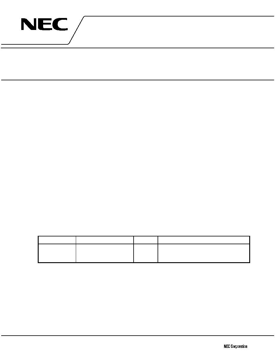
2
µ
µ
µ
µ
PC2776TB
6
1
4
3
5
2
PIN CONNECTIONS
PRODUCT LINE-UP OF
µ
µ
µ
µ
PC2776 (T
A
= +25 ∞C, V
CC
= V
out
= 5.0 V, Z
L
= Z
S
= 50
)
PART NO.
f
u
(GHz)
P
O (1dB)
(dBm)
P
O (sat)
(dBm)
G
P
(dB)
NF
(dB)
I
CC
(mA)
PACKAGE
MARKING
µ
PC2776T
6-pin minimold
µ
PC2776TB
6-pin super minimold
Remarks Typical performance. Please refer to ELECTRICAL CHARACTERISTICS in detail.
Notice The package size distinguishes between minimold and super minimold.
Selection point among product line-up
µ
PC2709TB: Suits to 1 GHz 2.5 GHz operation due to small inductance (e.g. 10 nH) between V
CC
and output pin.
µ
PC2776TB: Suits to HF to 2.0 GHz operation due to large inductance (e.g. 100 nH) between V
CC
and output pin.
PIN FUNCTIONS
PIN.
SYMBOL
APPLIED
VOLTAGE
(V)
DESCRIPTION
EQUIVALENT CIRCUIT
1
INPUT
-
High-frequency signal input pin. A in-
ternal matching circuit, configured with
resistors, enables 50
connection over
a wide band. A multi-feedback circuit is
designed to cancel the deviations of h
FE
and resistance.
2
3
5
GND
0
Ground pin. Form a ground pattern as
wide as possible to maintain the mini-
mum ground impedance.
4
OUTPUT
4.5 to 5.5
High-frequency signal output pin.
Connect an inductor between this pin
and V
CC
to supply current to the internal
output transistors.
6
V
CC
Power supply pin, which biases the in-
ternal input transistor.
Excellent RF characteristics are ob-
tained by a two-stage amplifier circuit.
To know the associated products, please refer to each latest data sheet.
25
6
23
+8.5
+6.5
C2L
2.7
(Top View)
3
2
1
4
5
6
(Bottom View)
4
5
6
3
2
1
C2L
Pin NO.
Pin name
1
INPUT
2
GND
3
GND
4
OUTPUT
5
GND
6
V
CC

3
µ
µ
µ
µ
PC2776TB
ABSOLUTE MAXIMUM RATINGS
PARAMETER
SYMBOL
CONDITION
RATINGS
UNIT
Supply voltage
V
CC
T
A
= +25 ∞C
6
V
Total circuit current
I
CC
T
A
= +25 ∞C
60
mA
Power dissipation
P
D
Mounted on 50
◊
50
◊
1.6 mm epoxy glass
PWB (T
A
= +85 ∞C)
200
mW
Operating ambient temperature
T
A
-
40 to +85
∞C
Storage temperature
T
STG
-
55 to +150
∞C
RECOMMENDED OPERATING CONDITIONS
PARAMETER
SYMBOL
MIN.
TYP.
MAX.
UNIT
NOTICE
Supply Voltage
V
CC
4.5
5.0
5.5
V
The same voltage should be ap-
plied to pin 4 and 6 pin.
Operating Ambient Temperature
T
A
-
40
+25
+85
∞C
ELECTRICAL CHARACTERISTICS (T
A
= +25 ∞C, V
CC
= V
out
= 5.0 V, Z
S
= Z
L
= 50
)
PARAMETER
SYMBOL
TEST CONDITION
MIN.
TYP.
MAX.
UNIT
Circuit current
I
CC
No signals
18
25
33
mA
Power gain
G
P
f = 1 GHz
21
23
26
dB
Output 1 dB compression level
P
O (1dB)
f = 1 GHz
+4.0
+6.5
-
dBm
Noise figure
NF
f = 1 GHz
-
6.0
7.5
dB
Upper limit operating frequency
f
u
3 dB down below from gain at
f = 100 MHz
2.3
2.7
-
GHz
Isolation
ISL
f = 1 GHz
27
32
-
dB
Input return loss
RL
in
f = 1 GHz
4.5
7.5
-
dB
Output return loss
RL
out
f = 1 GHz
15
20
-
dB
STANDARD CHARACTERISTICS FOR REFERENCE (T
A
= +25
∞
∞
∞
∞
C, V
CC
= V
out
= 5.0 V, Z
L
= Z
S
= 50
)
PARAMETER
SYMBOL
TEST CONDITION
REFERENCE
UNIT
Gain flatness
G
P
f = 0.1 to 2.0 GHz
±
1
dB
Saturated output power
P
O(sat)
f = 1 GHz
+8.5
dBm
3rd order intermodulation distortion
IM
3
P
O(each)
=
+ 0 dBm,
f
1
= 1000 MHz, f
2
= 1002 MHz
-
30
dBc
4
µ
µ
µ
µ
PC2776TB
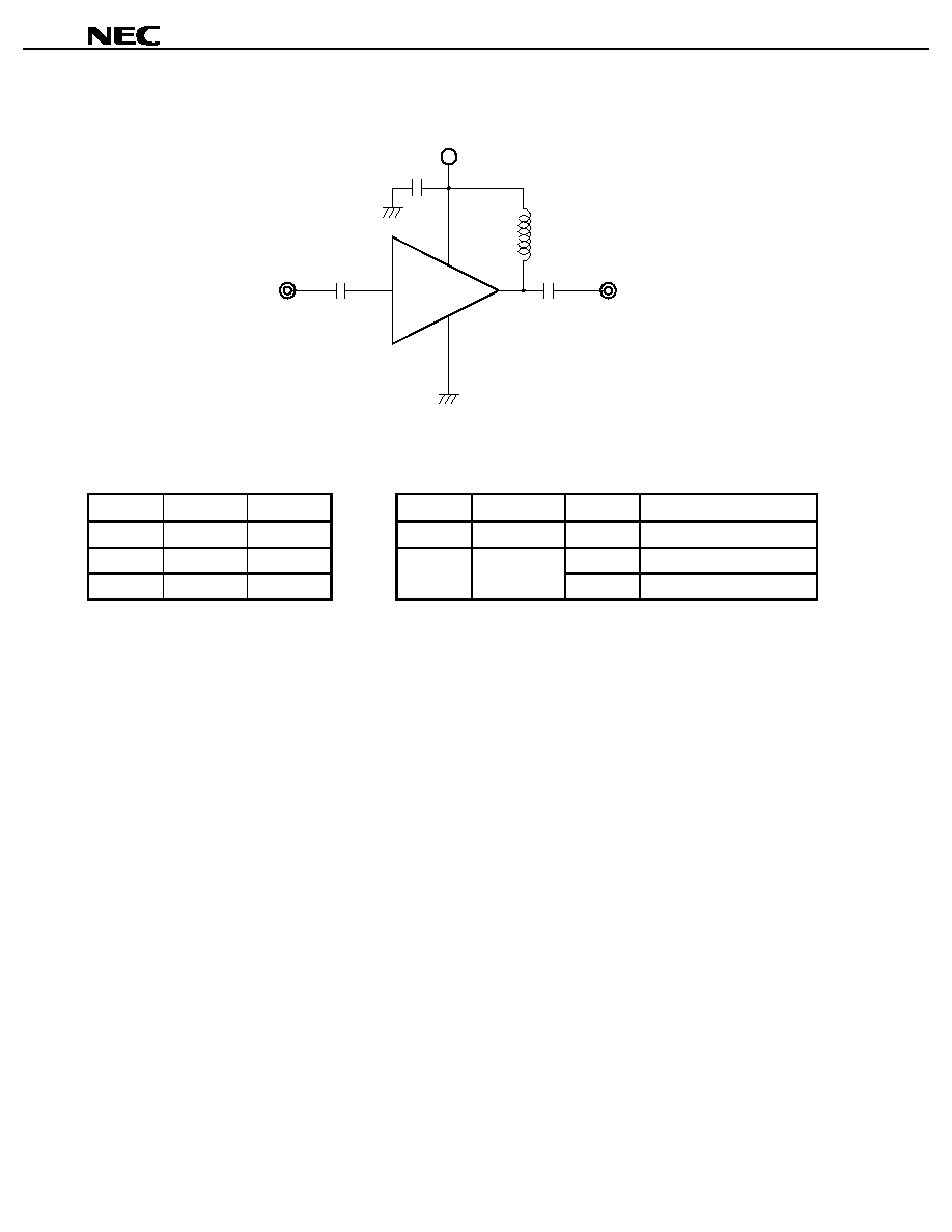
TEST CIRCUIT
V
CC
1 000 pF
1 000 pF
1 000 pF
C
1
C
2
L
4
6
1
2, 3, 5
50
50
OUT
IN
C
3
Components of test circuit for
measuring electrical characteristics
Example of actural application components
TYPE
VALUE
TYPE
VALUE
OPERATING FREQUENCY
C
3
Capacitor
1 000 pF
C
1
to C
3
Chip capacitor
1 000 pF
100 MHz or higher
L
Bias Tee
1 000 nH
L
Chip inductor
100 nH
100 MHz or higher
C
1
to C
2
Bias Tee
1 000 pF
10 nH
1.0 GHz or higher
INDUCTOR FOR THE OUTPUT PIN
The internal output transistor of this IC consumes 20 mA, to output medium power. To supply current for output
transistor, connect an inductor between the V
CC
pin (pin 6) and output pin (pin 4). Select large value inductance, as
listed above.
The inductor has both DC and AC effects. In terms of DC, the inductor biases the output transistor with minimum
voltage drop to output enable high level. In terms of AC, the inductor make output-port impedance higher to get
enough gain. In this case, large inductance and Q is suitable.
CAPACITORS FOR THE V
CC
, INPUT, AND OUTPUT PINS
Capacitors of 1 000 pF are recommendable as the bypass capacitor for the V
CC
pin and the coupling capacitors
for the input and output pins.
The bypass capacitor connected to the V
CC
pin is used to minimize ground impedance of V
CC
pin. So, stable bias
can be supplied against V
CC
fluctuation.
The coupling capacitors, connected to the input and output pins, are used to cut the DC and minimize RF serial
impedance. Their capacitance are therefore selected as lower impedance against a 50
load. The capacitors thus
perform as high pass filters, suppressing low frequencies to DC.
To obtain a flat gain from 100 MHz upwards, 1 000 pF capacitors are used in the test circuit. In the case of under
10 MHz operation, increase the value of coupling capacitor such as 10 000 pF. Because the coupling capacitors are
determined by equation, C = 1/(2
Rfc).

5
µ
µ
µ
µ
PC2776TB
Illustration of the application circuit assembled on evaluation board
IN
OUT
C
V
CC
C2L
3
2
1
4
5
6
Top View
Mounting direction
AMP-2
C
C
L
Notes
1. 30
◊
30
◊
0.4 mm double sided copper clad polyimide board.
2. Back side: GND pattern
3. Solder plated on pattern
4. : Through holes
Component List
Value
C
1 000 pF
L
100 nH, etc