©
2001
BIPOLAR ANALOG INTEGRATED CIRCUIT
µ
µ
µ
µ
PC2933A,
2905A
THREE-TERMINAL LOW DROPOUT VOLTAGE REGULATOR
DATA SHEET
Document No. G15374EJ2V0DS00 (2nd edition)
Date Published September 2001 NS CP(K)
Printed in Japan
The information in this document is subject to change without notice. Before using this document, please
confirm that this is the latest version.
Not all devices/types available in every country. Please check with local NEC representative for
availability and additional information.
DESCRIPTION
The
µ
PC2933A, 2905A of low dropout voltage three terminal positive regulators is constructed with PNP output
transistor. The
µ
PC2933A, 2905A feature the ability to source 1 A of output current with a low dropout voltage of typically
0.7 V.
The power dissipation of the
µ
PC2933A, 2905A can be drastically reduced compared with the conventional three
terminal positive voltage regulators that is constructed with NPN output transistor. Also, this series corresponds to the low
voltage output (3 V, 3.3 V) which is not in the conventional low dropout regulators (
µ
PC2400A series).
FEATURES
∑
Output current in excess of 1.0 A
∑
Low dropout voltage V
DIF
= 0.7 V TYP. (at I
O
= 1 A)
∑
On-chip overcurrent and thermal protection circuit
∑
∑
∑
∑
On-chip output transistor safe area protection circuit
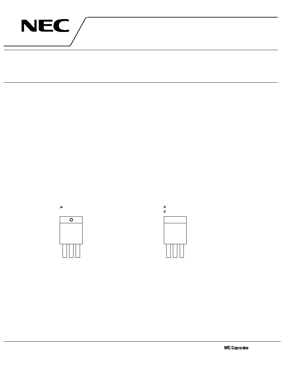
PIN CONFIGURATION (Marking Side)
1
2
3
1: INPUT
2: GND
3: OUTPUT
PC2933AHF, 2905AHF : MP-45G
1: INPUT
2: GND
3: OUTPUT
4: GND (Fin)
PC2933AHB, 2905AHB : MP-3
PC2933AT, 2905AT : MP-3Z
1
2
3
4
The mark
5
shows major revised points.
Data Sheet G15374EJ2V0DS
2
µ
µ
µ
µ
PC2933A,
2905A
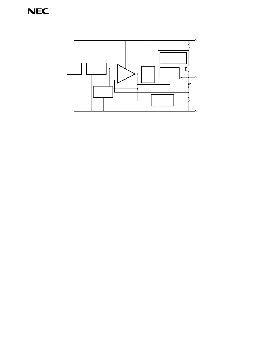
BLOCK DIAGRAM
Start-up
circuit
Reference
voltage
Thermal
shut down
Error
amp.
Drive
circuit
Saturation
protection
Safe operating
area protection
OUTPUT
GND
INPUT
Over current
protection

Data Sheet G15374EJ2V0DS
3
µ
µ
µ
µ
PC2933A,
2905A
ORDERING INFORMATION
Part Number
Package
Output Voltage
Marking
Package Type
µ
PC2933AHF
MP-45G
(Isolated TO-220)
3.3 V
2933A
∑
Packed in envelope
µ
PC2933AHB
MP-3 (SC-64)
3.3 V
2933A
∑
Packed in envelope
µ
PC2933AT
MP-3Z (SC-63)
3.3 V
2933A
∑
Packed in envelope
µ
PC2933AT-E1
MP-3Z (SC-63)
3.3 V
2933A
∑
16 mm wide embossed taping
∑
Pin 1 on drawout side
∑
2000 pcs/reel
µ
PC2933AT -E2
MP-3Z (SC-63)
3.3 V
2933A
∑
16 mm width embossed taping
∑
Pin 1 at takeup side
∑
2000 pcs/reel
µ
PC2933AT -T1
MP-3Z (SC-63)
3.3 V
2933A
∑
32 mm wide adhesive taping
∑
Pin 1 at drawout side
∑
1500 pcs/reel
µ
PC2933AT -T2
MP-3Z (SC-63)
3.3 V
2933A
∑
32 mm wide adhesive taping
∑
Pin 1 at takeup side
∑
1500 pcs/reel
µ
PC2905AHF
MP-45G
(Isolated TO-220)
5.0 V
2905A
∑
Packed in envelope
µ
PC2905AHB
MP-3 (SC-64)
5.0 V
2905A
∑
Packed in envelope
µ
PC2905AT
MP-3Z (SC-63)
5.0 V
2905A
∑
Packed in envelope
µ
PC2905AT-E1
MP-3Z (SC-63)
5.0 V
2905A
∑
16 mm wide embossed taping
∑
Pin 1 at drawout side
∑
2000 pcs/reel
µ
PC2905AT-E2
MP-3Z (SC-63)
5.0 V
2905A
∑
16 mm wide embossed taping
∑
Pin 1 at takeup side
∑
2000 pcs/reel
µ
PC2905AT-T1
MP-3Z (SC-63)
5.0 V
2905A
∑
32 mm wide adhesive taping
∑
Pin 1 at drawout side
∑
1500 pcs/reel
µ
PC2905AT-T2
MP-3Z (SC-63)
5.0 V
2905A
∑
32 mm wide adhesive taping
∑
Pin 1 at takeup side
∑
1500 pcs/reel
Data Sheet G15374EJ2V0DS
4
µ
µ
µ
µ
PC2933A,
2905A
ABSOLUTE MAXIMUM RATINGS (T
A
= 25∞C unless otherwise specified)
Rating
Parameter
Symbol
µ
PC2933AHF,
2905AHF
µ
PC2933AHB, 2905AHB
µ
PC2933AT, 2905AT
Unit
Input Voltage
V
IN
20
V
Internal Power Dissipation
Note
(T
C
= 25
∞
C)
P
T
15
10
W
Operating Ambient Temperature
T
A
≠30 to +85
∞C
Operating Junction Temperature
T
J
≠30 to +150
∞C
Storage Temperature
T
stg
≠55 to +150
∞C
Thermal Resistance (junction to case)
R
th(J-C)
7
12.5
∞C/W
Thermal Resistance (junction to ambient)
R
th(J-A)
65
125
∞C/W
Note Internally limited. When the operating junction temperature rises over 150
∞
C, the internal circuit shuts down the
output voltage.
Caution If the absolute maximum rating of any of the above parameters is exceeded even momentarily, the
quality of the product may be degraded. In other words, absolute maximum ratings specify the
values exceeding which the product may be physically damaged. Be sure to use the product with
these ratings never exceeded.
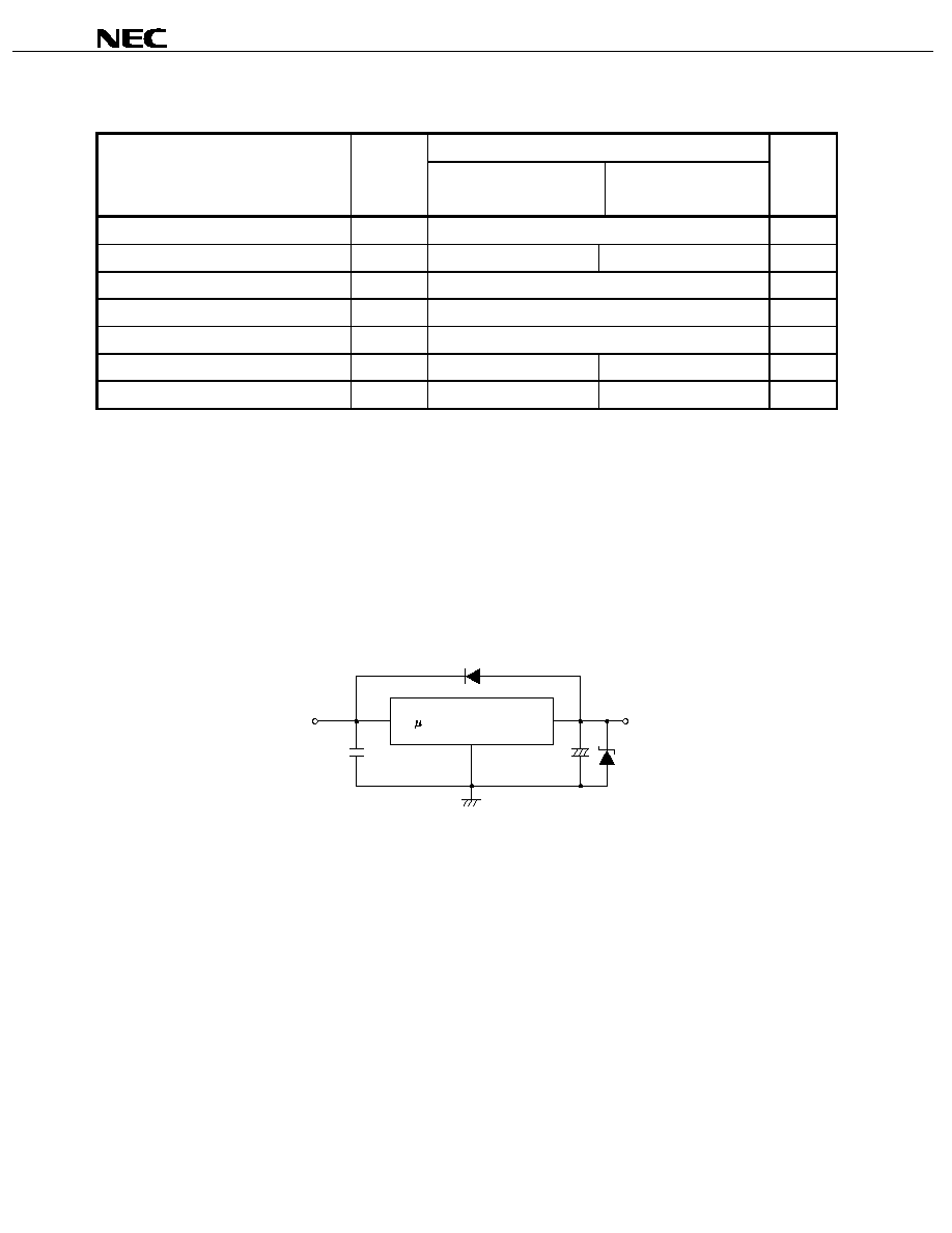
STANDARD CONNECTION
INPUT
C
IN
PC2933A, 2905A
OUTPUT
C
OUT
D
1
D
2
+
C
IN
: 0.1
µ
F or higher. Set this value according to the length of the line between the regulator and INPUT pin. Be sure
to connect C
IN
to prevent parasitic oscillation. Use of a film capacitor or other capacitor with excellent voltage and
temperature characteristics is recommended. If using a laminated ceramic capacitor, it is necessary to ensure
that C
IN
is 0.1
µ
F or higher for the voltage and temperature range to be used.
C
OUT
: 47
µ
F or higher. Be sure to connect C
OUT
to prevent oscillation and improve excessive load regulation. Place
C
IN
and C
OUT
as close as possible to the IC pins (within 2 cm). Also, use an electrolytic capacitor with low
impedance characteristics if considering use at sub-zero temperatures.
D
1
: If the OUTPUT pin has a higher voltage than the INPUT pin, connect a diode.
D
2
: If the OUTPUT pin has a lower voltage than the GND pin, connect a Schottky barrier diode.
Caution Make sure that no voltage is applied to the OUTPUT pin from external.
5
Data Sheet G15374EJ2V0DS
5
µ
µ
µ
µ
PC2933A,
2905A
RECOMMENDED OPERATING CONDITIONS
Parameter
Symbol
Type Number
MIN.
TYP.
MAX.
Unit
µ
PC2933A
4.3
16
Input Voltage
V
IN
µ
PC2905A
6
16
V
Output Current
I
O
All
0
1.0
A
Operating Ambient Temperature T
A
All
≠30
+85
∞
C
Operating Junction Temperature T
J
All
≠30
+125
∞
C
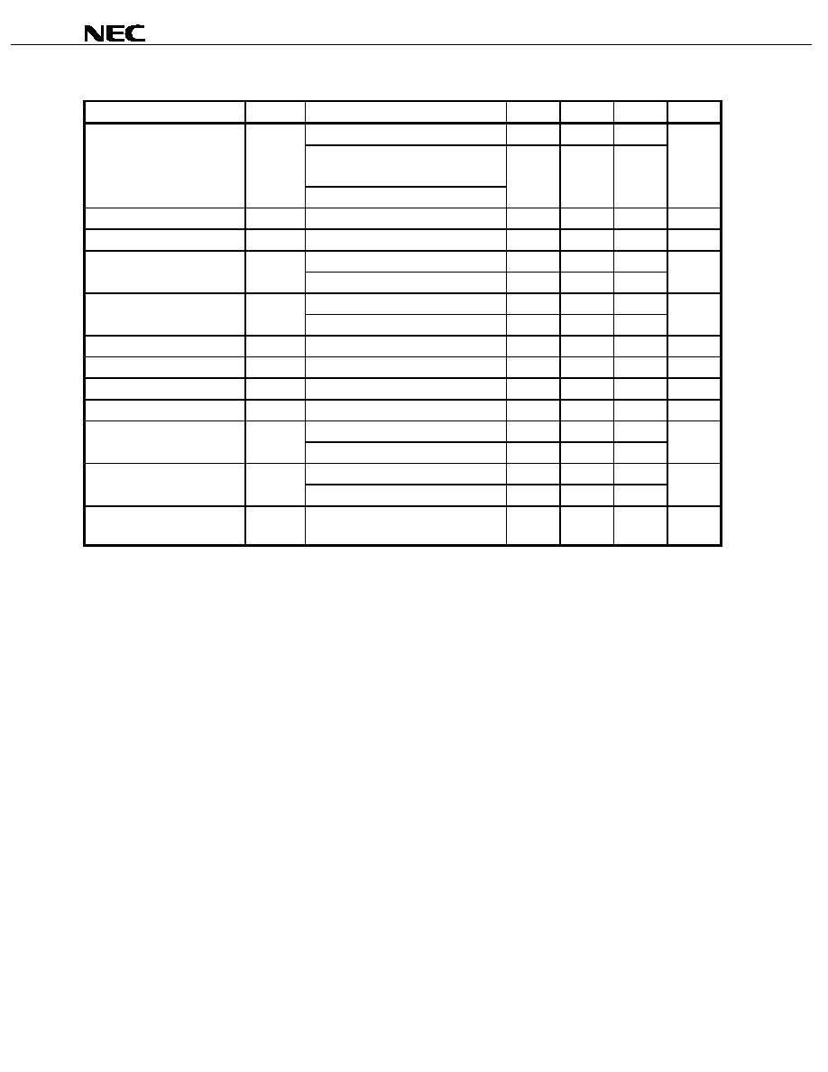
ELECTRICAL CHARACTERISTICS
µ
µ
µ
µ
PC2933A
(T
J
= 25
∞
∞
∞
∞
C, V
IN
= 5 V, I
O
= 500 mA, C
IN
= 0.22
µ
µ
µ
µ
F, C
OUT
= 47
µ
µ
µ
µ
F, unless otherwise specified)
Parameter
Symbol
Conditions
MIN.
TYP.
MAX.
Unit
3.18
3.3
3.42
V
Output Voltage
V
O
0
∞
C
T
J
125
∞
C, 4.3 V
V
IN
16 V,
0 A
I
O
500 mA
3.14
3.46
0
∞
C
T
J
125
∞
C, 0 A
I
O
1 A
Line Regulation
REG
IN
4.3 V
V
IN
16 V
12
33
mV
Load Regulation
REG
L
0 A
I
O
1 A
23
33
I
O
= 0 A
2.0
3.0
mA
Quiescent Current
I
BIAS
I
O
= 1 A
20
40
V
IN
= 3.1 V, I
O
= 0 A
10
30
mA
Startup Quiescent Current
I
BIAS (s)
V
IN
= 3.1 V, I
O
= 1 A
80
Quiescent Current Change
I
BIAS
0
∞
C
T
J
125
∞
C, 4.3 V
V
IN
16 V
3.0
15
mA
Output Noise Voltage
V
n
10 Hz
f
100 kHz
55
µ
V
r.m.s.
Ripple Rejection
R∑R
4.3 V
V
IN
16 V, f = 120 Hz
48
64
dB
Dropout Voltage
V
DIF
0
∞
C
T
J
125
∞
C, I
O
= 1 A
0.7
1.0
V
V
IN
= 4.5 V
1.2
1.6
3.0
Short Circuit Current
I
Opeak
V
IN
= 16 V
1.2
A
V
IN
= 4.5 V
1.0
1.4
3.0
A
Peak Output Current
I
Opeak
V
IN
= 16 V
1.3
1.7
2.8
Temperature Coefficient of
Output Voltage
V
O
/
T
0
∞
C
T
J
125
∞
C, I
O
= 5 mA
≠0.4
mV/
∞
C
Data Sheet G15374EJ2V0DS
6
µ
µ
µ
µ
PC2933A,
2905A
µ
µ
µ
µ
PC2905A
(T
J
= 25
∞
∞
∞
∞
C, V
IN
= 8 V, I
O
= 500 mA, C
IN
= 0.22
µ
µ
µ
µ
F, C
OUT
= 47
µ
µ
µ
µ
F, unless otherwise specified)
Parameter
Symbol
Conditions
MIN.
TYP.
MAX.
Unit
4.83
5.0
5.18
V
Output Voltage
V
O
0
∞
C
T
J
125
∞
C, 6 V
V
IN
16 V,
0 A
I
O
500 mA
4.75
5.25
0
∞
C
T
J
125
∞
C, 0 A
I
O
1 A
Line Regulation
REG
IN
6 V
V
IN
16 V
23
50
mV
Load Regulation
REG
L
0 A
I
O
1 A
28
50
mV
I
O
= 0 A
2.2
3.5
mA
Quiescent Current
I
BIAS
I
O
= 1 A
28
50
V
IN
= 4.5 V, I
O
= 0 A
10
30
mA
Startup Quiescent Current
I
BIAS (s)
V
IN
= 4.5 V, I
O
= 1 A
50
Quiescent Current Change
I
BIAS
0
∞
C
T
J
125
∞
C, 6 V
V
IN
16 V
2.9
15
mA
Output Noise Voltage
V
n
10 Hz
f
100 kHz
90
µ
V
r.m.s.
Ripple Rejection
R∑R
f = 120 Hz, 6 V
V
IN
16 V
46
61
dB
Dropout Voltage
V
DIF
0
∞
C
T
J
125
∞
C, I
O
= 1 A
0.7
1.0
V
V
IN
= 6.5 V
1.15
1.8
3.0
Short Circuit Current
I
Opeak
V
IN
= 16 V
1.1
A
V
IN
= 6.5 V
1.1
1.5
3.0
A
Peak Output Current
I
Opeak
V
IN
= 16 V
1.4
2.0
2.8
Temperature Coefficient of
Output Voltage
V
O
/
T
0
∞
C
T
J
125
∞
C, I
O
= 5 mA
0.6
mV/
∞
C
Data Sheet G15374EJ2V0DS
7
µ
µ
µ
µ
PC2933A,
2905A
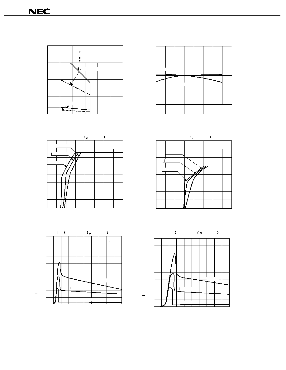
TYPICAL CHARACTERISTICS (Reference Values)
300
200
100
0
-100
-200
-300
-400
0
100
150
T
J
V - Output Voltage Deviation - mV
O
V
O
vs.T
J
-50
50
PC2905A
PC2933A
I
O
= 5 mA
-
Operating Junction Temperature - ∞C
µ
µ
4.0
3.5
3.0
2.5
2.0
1.5
1.0
0.5
0
0
1
2
3
4
5
6
7
8
V
IN
Voltage - V
V
O
- Output Voltage - V
V
O
vs.V
IN
PC2933A
T
J
= 25∞C
O
= 0.5 A
I
O
= 5 mA
I
O
= 1.0 A
- Input
8
7
6
5
4
3
2
1
0
0
1
2
3
4
5
6
7
8
V
IN
- Input Voltage - V
V
O
vs. V
IN
PC2905A
T
J
= 25∞C
O
= 0.5 A
I
O
= 5 mA
I
O
= 1.0 A
V
O
- Output Voltage - V
50
40
30
20
10
0
4
0
2
6
8
10
12
14
16
18
20
BIAS
Quiescent Current - mA
BIAS
I
BIAS(s)
) vs.V
IN
PC2933A
O
= 0.5 A
I
O
= 0 A
I
O
= 1 A
T = 25∞C
V
IN
- Input Voltage - V
50
40
30
20
10
0
2
4
6
8
10
12
14
16
18
20
T = 25
∞C
O
= 0.5 A
I
O
= 0 A
I
O
= 1 A
V
IN
- Input Voltage - V
BIAS
I
BIAS(s)
) vs.V
IN
PC2905A
B
IA
S
Quiescent Current - mA
50
85 100
150
5
10
15
20
0
1.0
1.92
P
d -
T
otal P
o
w
er Dissipation -
W
T
A -
Operating Ambient Temperature - ∞C
0
P
d vs.
T
A
Solid line :
PC2933AHF, 2905AHF
Broken line :
PC2933AHB, 2905AHB
PC2933AT, 2905AT
With infinite heatsink
Without heatsink

Data Sheet G15374EJ2V0DS
8
µ
µ
µ
µ
PC2933A,
2905A
1.0
0.8
0.6
0.4
0.2
0
-25
+125
0
+150
+75
V
DIF
- Dropout Voltage - V
V
DIF
vs.T
J
+100
+50
+25
PC2905A
PC2933A
I
O
= 1.0 A
T
J
Operating Junction Temperature - ∞C
3
2
1
0
0
20
DIF
I
O peak
- Peak Output Current - A
I
O peak
vs. V
DIF
PC2933A
10
15
5
T
J
= 125∞C
T
J
= 25∞C
T
J
= 0∞C
- Dropout Voltage - V
V
m
3
2
1
0
0
20
I
O peak
- Peak Output Current - A
vs.V
I
O peak
DIF
PC2905A
10
15
T
J
= 125∞C
T
J
= 25∞C
T
J
= 0∞C
V
DIF
- Dropout Voltage - V
R
R vs. f
R
R - Ripple Rejection - dB
80
70
0
100
1 k
10 k
100 k
f - Frequency - Hz
60
50
40
30
20
10
T
J
= 25∞C
I
O
= 1 A
PC2933A
PC2905A
4.3 V
V
IN
16 V
6 V
V
IN
16 V ( PC2905A)
( PC2933A)
R
R vs. I
O
80
70
30
0.2
0.4
0.6
1.0
0.8
0
60
50
40
PC2933A
PC2905A
O
- Output Current - A
I
R
R - Ripple Rejection - dB
f = 120 Hz
T
J
= 25∞C
4.3 V
V
IN
16 V
6 V
V
IN
16 V ( PC2905A)
( PC2933A)
V
DIF
vs. I
O
V
DIF
- Dropout Voltage - V
1.0
0
0.2
0.4
0.6
1.0
I
O
- Output Current - A
0.8
0.6
0.4
0.2
0
0.8
PC2905A
PC2933A
T
J
= 25∞C
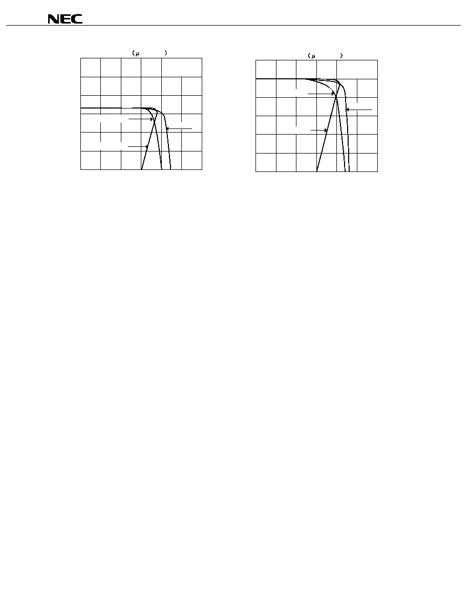
Data Sheet G15374EJ2V0DS
9
µ
µ
µ
µ
PC2933A,
2905A
V
O
vs.I
O
PC2933A
6
5
0
0.4
0.8
1.2
2.4
1.6
4
3
1
2.0
2
V
IN
= 16 V
V
IN
= 4.3 V
V
IN
= 5 V
T
J
= 25∞C
I
O
- Output Current - A
V
O
- Output Voltage - V
6
5
0
0.4
0.8
1.2
2.4
1.6
4
3
1
2.0
2
V
IN
= 16 V
V
IN
= 6 V
V
IN
= 8 V
V
O
vs.I
O
PC2905A
V
O
- Output Voltage - V
I
O
- Output Current - A
T
J
= 25∞C

Data Sheet G15374EJ2V0DS
10
µ
µ
µ
µ
PC2933A,
2905A
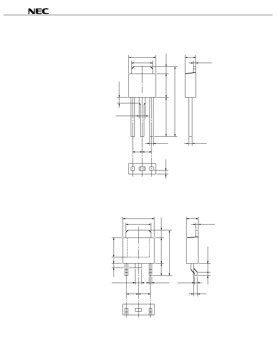
PACKAGE DRAWINGS
µ
µ
µ
µ
PC2933AHF, 2905AHF
D
17.0
±
0.3
3PIN PLASTIC SIP (MP-45G)
NOTE
Each lead centerline is located within 0.25 mm of
its true position (T.P.) at maximum material condition.
ITEM
MILLIMETERS
P3HF-254B-4
G
0.25
H
2.54 (T.P.)
A
10.0
±
0.2
I
5.0
±
0.3
U
2.4
±
0.5
V
Y
8.9
±
0.7
Z
1.30
±
0.2
J
K
L
8.5
±
0.2
B
7.0
±
0.2
C
1.50
±
0.2
E
F
0.75
±
0.10
M
8.5
±
0.2
N
P
2.8
±
0.2
3.3
±
0.2
2.46
±
0.2
5.0
±
0.2
4.5
±
0.2
0.65
±
0.10
1
3
2
M
A
B
E
I
D
L
M
K
Y
J
H
C
F
G
Z
N
P
U
V
Data Sheet G15374EJ2V0DS
11
µ
µ
µ
µ
PC2933A,
2905A
µ
µ
µ
µ
PC2933AHB, 2905AHB
MP-3 (SC-64) (Unit: mm)
1
2
3
4
2.3
2.3
0.75
1.1
±0.1
0.5
1.6
±
0.2
5.0
±0.2
6.5 0.2
5.5
±
0.2
7.0 MIN.
+
0.2
≠
0.1
1.5
+
0.
2
≠
0.
1
13.7 MIN.
2.3
±
0.2
0.5
±0.1
0.5
+
0.2
≠
0.1
±
µ
µ
µ
µ
PC2933AT, 2905AT
MP-3Z (SC-63) (Unit: mm )
2.3
2.3
0.8
0.9 MAX.
0.8 MAX.
1.1±0.2
0.8
1
2
3
4
4.3 MAX.
10.0 MAX.
0.5
1.0 MIN.
1.5 TYP.
2.0 MIN.
5.5
±
0.2
1.5
+
0.2
≠
0.1
6.5±0.2
2.3±0.2
5.0±0.2
0.5±0.1
Data Sheet G15374EJ2V0DS
12
µ
µ
µ
µ
PC2933A,
2905A
RECOMMENDED SOLDERING CONDITIONS
When soldering this product, it is highly recommended to observe the conditions as shown below. If other soldering
processes are used, or if the soldering is perfomed under different condition, please make sure to consult with our
sales offices.
For more details, refer to our document "SEMICONDUCTOR DEVICE MOUNTING TECHNOLOGY MANUAL"
(C10535E).
Surface Mount Device
µ
µ
µ
µ
PC2933AT, 2905AT: MP-3Z (SC-63)
Process
Conditions
Symbol
Infrared Ray Reflow
Peak temperature: 235∞C or below (Package surface temperature),
Reflow time: 30 seconds or less (at 210∞C or higher),
Maximum number of reflow processes: 2 times or less.
IR35-00-2
Vapor Phase Soldering
Peak temperature: 215∞C or below (Package surface temperature),
Reflow time: 40 seconds or less (at 200∞C or higher),
Maximum number of reflow processes: 2 times or less.
VP15-00-2
Wave Soldering
Solder temperature: 260∞C or below, Flow time: 10 seconds or less,
Maximum number of flow processes: 1 time,
Pre-heating temperature: 120∞C or below (Package surface temperature).
WS60-00-1
Partial Heating Method
Pin temperature: 300∞C or below,
Heat time: 3 seconds or less (Per each side of the device).
≠
Caution Apply only one kind of soldering condition to a device, except for "partial heating method", or the
device will be damaged by heat stress.
Through-hole devices
µ
PC2933AHF, 2905AHF: MP-45G
µ
PC2933AHB, 2905AHB: MP-3
Process
Conditions
Wave soldering
(only to leads)
Solder temperature: 260∞C or below,
Flow time: 10 seconds or less.
Partial heating method
Pin temperature: 300∞C or below,
Heat time: 3 seconds or less (Per each pin).
Caution For through-hole device, the wave soldering process must be applied only to leads, and make
sure that the package body does not get jet soldered.
Data Sheet G15374EJ2V0DS
13
µ
µ
µ
µ
PC2933A,
2905A
NOTES ON USE
When the
µ
PC2933A, 2905A are used with an input voltage that is lower than the value indicated in the recommended
operating conditions, a large quiescent current flows through the device due to saturation of the transistor of the output
stage. (Refer to the I
BIAS
(I
BIAS(S)
) vs. V
IN
curves in TYPICAL CHARACTERISTICS).
These products have saturation protector, but a current of up to 80 mA MAX. may flow through the device. Thus the
power supply on the input side must have sufficient capacity to allow this quiescent current to pass when the device starts
up.
REFERENCE DOCUMENTS
Document Name
Document No.
QUALITY GRADES ON NEC SEMICONDUCTOR DEVICES
C11531E
SEMICONDUCTOR DEVICE MOUNTING TECHNOLOGY MANUAL
C10535E
VOLTAGE REGULATOR OF SMD
G11872E
SEMICONDUCTOR SELECTION GUIDE ≠ PRODUCTS AND PACKAGES
X13769E

Data Sheet G15374EJ2V0DS
14
µ
µ
µ
µ
PC2933A,
2905A
[MEMO]

Data Sheet G15374EJ2V0DS
15
µ
µ
µ
µ
PC2933A,
2905A
[MEMO]

µ
µ
µ
µ
PC2933A,
2905A
M8E 00. 4
The information in this document is current as of September, 2001. The information is subject to
change without notice. For actual design-in, refer to the latest publications of NEC's data sheets or
data books, etc., for the most up-to-date specifications of NEC semiconductor products. Not all
products and/or types are available in every country. Please check with an NEC sales representative
for availability and additional information.
No part of this document may be copied or reproduced in any form or by any means without prior
written consent of NEC. NEC assumes no responsibility for any errors that may appear in this document.
NEC does not assume any liability for infringement of patents, copyrights or other intellectual property rights of
third parties by or arising from the use of NEC semiconductor products listed in this document or any other
liability arising from the use of such products. No license, express, implied or otherwise, is granted under any
patents, copyrights or other intellectual property rights of NEC or others.
Descriptions of circuits, software and other related information in this document are provided for illustrative
purposes in semiconductor product operation and application examples. The incorporation of these
circuits, software and information in the design of customer's equipment shall be done under the full
responsibility of customer. NEC assumes no responsibility for any losses incurred by customers or third
parties arising from the use of these circuits, software and information.
While NEC endeavours to enhance the quality, reliability and safety of NEC semiconductor products, customers
agree and acknowledge that the possibility of defects thereof cannot be eliminated entirely. To minimize
risks of damage to property or injury (including death) to persons arising from defects in NEC
semiconductor products, customers must incorporate sufficient safety measures in their design, such as
redundancy, fire-containment, and anti-failure features.
NEC semiconductor products are classified into the following three quality grades:
"Standard", "Special" and "Specific". The "Specific" quality grade applies only to semiconductor products
developed based on a customer-designated "quality assurance program" for a specific application. The
recommended applications of a semiconductor product depend on its quality grade, as indicated below.
Customers must check the quality grade of each semiconductor product before using it in a particular
application.
"Standard": Computers, office equipment, communications equipment, test and measurement equipment, audio
and visual equipment, home electronic appliances, machine tools, personal electronic equipment
and industrial robots
"Special":
Transportation equipment (automobiles, trains, ships, etc.), traffic control systems, anti-disaster
systems, anti-crime systems, safety equipment and medical equipment (not specifically designed
for life support)
"Specific": Aircraft, aerospace equipment, submersible repeaters, nuclear reactor control systems, life
support systems and medical equipment for life support, etc.
The quality grade of NEC semiconductor products is "Standard" unless otherwise expressly specified in NEC's
data sheets or data books, etc. If customers wish to use NEC semiconductor products in applications not
intended by NEC, they must contact an NEC sales representative in advance to determine NEC's willingness
to support a given application.
(Note)
(1) "NEC" as used in this statement means NEC Corporation and also includes its majority-owned subsidiaries.
(2) "NEC semiconductor products" means any semiconductor product developed or manufactured by or for
NEC (as defined above).
∑
∑
∑
∑
∑
∑