 | –≠–ª–µ–∫—Ç—Ä–æ–Ω–Ω—ã–π –∫–æ–º–ø–æ–Ω–µ–Ω—Ç: UPC29M07T | –°–∫–∞—á–∞—Ç—å:  PDF PDF  ZIP ZIP |
©
1997
DATA SHEET
BIPOLAR ANALOG INTEGRATED CIRCUIT
µ
PC29M00 Series
THREE TERMINAL LOW DROPOUT VOLTAGE REGULATOR
The
µ
PC29M00 series of low dropout voltage three terminal positive regulators is constructed with PNP output
transistor. The
µ
PC29M00 series feature the ability to source 0.5 A of output current with a low dropout voltage of
typically 0.5 V.
The power dissipation of the
µ
PC29M00 series can be drastically reduced compared with the conventional three
terminal positive voltage regulators that is constructed with NPN output transistor. Also, this series corresponds to
the low voltage output (3 V, 3.3 V) which is not in the conventional low dropout regulators (
µ
PC24M00A series).
FEATURES
∑
Output current in excess of 0.5 A
∑
Low dropout voltage V
DIF
= 0.5 V TYP. (at I
O
= 0.5 A)
∑
On-chip overcurrent and thermal protection circuit
∑
On-chip output transistor safe area protection circuit
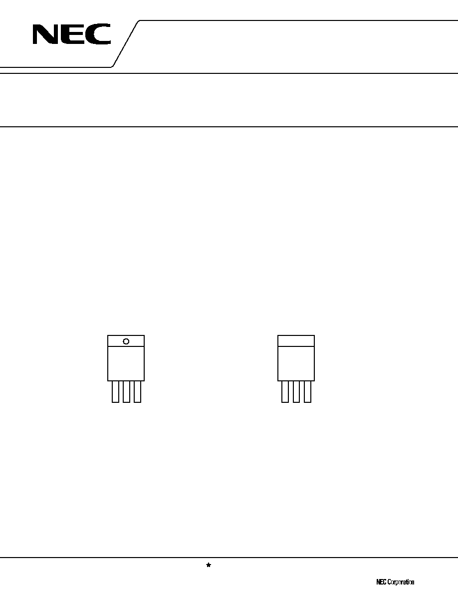
PIN CONFIGURATION (Marking Side)
µ
PC29M00HF Series: MP-45G
µ
PC29M00HB Series: MP-3
µ
PC29M00T Series: MP-3Z
1
2
1: INPUT
2: GND
3: OUTPUT
3
1
2
1: INPUT
2: GND
3: OUTPUT
4: GND (Fin)
3
4
Document No. G10027EJ3V0DS00 (3rd edition)
Date Published July 1998 N CP(K)
Printed in Japan
The information in this document is subject to change without notice.
The mark shows major revised points.

µ
PC29M00 Series
2
BLOCK DIAGRAM
Start-up
circuit
Reference
voltage
Thermal
shut down
Error
amp.
Drive
circuit
Saturation
protection
Safe operating
area protection
OUTPUT
GND
INPUT
Over current
protection
ORDERING INFORMATION
Part Number
Package
Output Voltage
µ
PC29M03HF
MP-45G (Isolated TO-220)
3.0 V
µ
PC29M03HB
MP-3 (SC-64)
3.0 V
µ
PC29M03T
MP-3Z (SC-63)
3.0 V
µ
PC29M33HF
MP-45 (Isolated TO-220)
3.3 V
µ
PC29M33HB
MP-3 (SC-64)
3.3 V
µ
PC29M33T
MP-3Z (SC-63)
3.3 V
µ
PC29M05HF
MP-45G (Isolated TO-220)
5.0 V
µ
PC29M05HB
MP-3 (SC-64)
5.0 V
µ
PC29M05T
MP-3Z (SC-63)
5.0 V
µ
PC29M06HF
MP-45G (Isolated TO-220)
6.0 V
µ
PC29M06HB
MP-3 (SC-64)
6.0 V
µ
PC29M06T
MP-3Z (SC-63)
6.0 V
µ
PC29M07HF
MP-45G (Isolated TO-220)
7.0 V
µ
PC29M07HB
MP-3 (SC-64)
7.0 V
µ
PC29M07T
MP-3Z (SC-63)
7.0 V
µ
PC29M08HF
MP-45G (Isolated TO-220)
8.0 V
µ
PC29M08HB
MP-3 (SC-64)
8.0 V
µ
PC29M08T
MP-3Z (SC-63)
8.0 V
µ
PC29M09HF
MP-45G (Isolated TO-220)
9.0 V
µ
PC29M09HB
MP-3 (SC-64)
9.0 V
µ
PC29M09T
MP-3Z (SC-63)
9.0 V
µ
PC29M10HF
MP-45G (Isolated TO-220)
10.0 V
µ
PC29M10HB
MP-3 (SC-64)
10.0 V
µ
PC29M10T
MP3Z (SC-63)
10.0 V
µ
PC29M12HF
MP-45G (Isolated TO-220)
12.0 V
µ
PC29M12HB
MP-3 (SC-64)
12.0 V
µ
PC29M12T
MP-3Z (SC-63)
12.0 V

µ
PC29M00 Series
3
ABSOLUTE MAXIMUM RATINGS (T
A
= 25
∞
C, Unless otherwise specified.)
Parameter
Symbol
Rating
Unit
µ
PC29M00HF
µ
PC29M00HB,
µ
PC29M00T
Input Voltage
V
IN
20
V
Internal Power Dissipation
Note
P
T
15
10
W
Operating Ambient Temperature
T
A
≠30 to +85
∞
C
Operating Junction Temperature
T
J
≠30 to +150
∞
C
Storage Temperature
T
stg
≠55 to +150
∞
C
Thermal Resistance (Junction to Case)
R
th (J-C)
7
12.5
∞
C/W
Thermal Resistance (Junction to Ambient)
R
th (J-A)
65
125
∞
C/W
Note T
C
= 25
∞
C, Internally limited
When operating junction temperature rises up to 150
∞
C, the internal circuit shutdown output voltage.
Caution Exposure to Absolute Maximum Ratings for extended periods may affect device reliability;
exceeding the ratings could cause permanent damage. The parameters apply independently. The
device should be operated within the limits specified under DC and AC Characteristics.
TYPICAL CONNECTION
D
1
PC29M00
INPUT
C
OUT
C
IN
D
2
+
µ
OUTPUT
C
IN
: More than 0.1
µ
F. Required if regulator is located an appreciable distance from power supply filter. You
must use to prevent from the parasitic oscillation.
C
OUT
: More than 47
µ
F. You must use the Low-impedance-type (low ESR) capacitor.
D
1
: Need for V
O
> V
IN
D
2
: Need a shottky barrier diode for V
O
< GND.

µ
PC29M00 Series
4
RECOMMENDED OPERATING CONDITIONS
Parameter
Symbol
Type Number
MIN.
TYP.
MAX.
Unit
Input Voltage
V
IN
µ
PC29M03
4
16
V
µ
PC29M33
4.3
16
µ
PC29M05
6
16
µ
PC29M06
7
16
µ
PC29M07
8
16
µ
PC29M08
9
18
µ
PC29M09
10
18
µ
PC29M10
11
18
µ
PC29M12
13
18
Output Current
I
O
all
0
0.5
A
Operating Ambient Temperature
T
A
all
≠30
+85
∞
C
Operating Junction Temperature
T
J
all
≠30
+125
∞
C
ELECTRICAL CHARACTERISTICS
µ
PC29M03 (T
J
= 25
∞
C, V
IN
= 5 V, I
O
= 350 mA, C
IN
= 0.22
µ
F, C
OUT
= 47
µ
F,
unless otherwise specified.)
Parameters
Symbol
Conditions
MIN.
TYP.
MAX.
Unit
Output Voltage
V
O
2.88
3.0
3.12
V
0
∞
C
T
J
125
∞
C, 4.0 V
V
IN
16 V,
2.85
3.15
0 A
I
O
350 mA
0
∞
C
T
J
125
∞
C, 0 A
I
O
0.5 A
Line Regulation
REG
IN
4.0 V
V
IN
16 V
7
30
mV
Load Regulation
REG
L
0 A
I
O
0.5 A
8
30
mV
Quiescent Current
I
BIAS
I
O
= 0 A
1.8
4.0
mA
I
O
= 0.5 A
17
30
Startup Quiescent Current
I
BIAS (s)
V
IN
= 2.95 V, I
O
= 0 A
7
30
mA
V
IN
= 2.95 V, I
O
= 0.5 A
80
Quiescent Current Change
I
BIAS
0
∞
C
T
J
125
∞
C, 4.0 V
V
IN
16 V
3.2
20
mA
Output Noise Voltage
V
n
10 Hz
f
100 kHz
51
µ
V
r.m.s.
Ripple Rejection
R∑R
f = 120 Hz, 4.0 V
V
IN
16 V
48
64
dB
Dropout Voltage
V
DIF
0
∞
C
T
J
125
∞
C, I
O
= 0.5 A
0.5
1.0
V
Short Circuit Current
I
O short
V
IN
= 4.5 V
0.65
1.0
1.5
A
V
IN
= 16 V
0.6
Peak Output Current
I
O peak
V
IN
= 4.5 V
0.7
1.0
1.5
A
V
IN
= 16 V
0.6
0.9
1.5
Temperature Coefficient of
V
O
/
T
0
∞
C
T
J
125
∞
C, I
O
= 5 mA
≠0.3
mV/
∞
C
Output Voltage

µ
PC29M00 Series
5
ELECTRICAL CHARACTERISTICS
µ
PC29M33 (T
J
= 25
∞
C, V
IN
= 5 V, I
O
= 350 mA, C
IN
= 0.22
µ
F, C
OUT
= 47
µ
F,
unless otherwise specified.)
Parameters
Symbol
Conditions
MIN.
TYP.
MAX.
Unit
Output Voltage
V
O
3.17
3.3
3.43
V
0
∞
C
T
J
125
∞
C, 4.3 V
V
IN
16 V,
3.14
3.46
0 A
I
O
350 mA
0
∞
C
T
J
125
∞
C, 0 A
I
O
0.5 A
Line Regulation
REG
IN
4.3 V
V
IN
16 V
8
33
mV
Load Regulation
REG
L
0 A
I
O
0.5 A
10
33
mV
Quiescent Current
I
BIAS
I
O
= 0 A
1.8
4.0
mA
I
O
= 0.5 A
15
30
Startup Quiescent Current
I
BIAS (s)
V
IN
= 3.1 V, I
O
= 0 A
9
30
mA
V
IN
= 3.1 V, I
O
= 0.5 A
80
Quiescent Current Change
I
BIAS
0
∞
C
T
J
125
∞
C, 4.3 V
V
IN
16 V
2.9
20
mA
Output Noise Voltage
V
n
10 Hz
f
100 kHz
56
µ
V
r.m.s.
Ripple Rejection
R∑R
f = 120 Hz, 4.3 V
V
IN
16 V
48
64
dB
Dropout Voltage
V
DIF
0
∞
C
T
J
125
∞
C, I
O
= 0.5 A
0.5
1.0
V
Short Circuit Current
I
O short
V
IN
= 4.5 V
0.7
1.1
1.5
A
V
IN
= 16 V
0.6
Peak Output Current
I
O peak
V
IN
= 4.5 V
0.7
1.2
1.5
A
V
IN
= 16 V
0.6
1.0
1.5
Temperature Coefficient of
V
O
/
T
0
∞
C
T
J
125
∞
C, I
O
= 5 mA
≠0.4
mV/
∞
C
Output Voltage

µ
PC29M00 Series
6
ELECTRICAL CHARACTERISTICS
µ
PC29M05 (T
J
= 25
∞
C, V
IN
= 8 V, I
O
= 350 mA, C
IN
= 0.22
µ
F, C
OUT
= 47
µ
F,
unless otherwise specified.)
Parameters
Symbol
Conditions
MIN.
TYP.
MAX.
Unit
Output Voltage
V
O
4.8
5.0
5.2
V
0
∞
C
T
J
125
∞
C, 6 V
V
IN
16 V,
4.75
5.25
0 A
I
O
350 mA
0
∞
C
T
J
125
∞
C, 0 A
I
O
0.5 A
Line Regulation
REG
IN
6 V
V
IN
16 V
26
50
mV
Load Regulation
REG
L
0 A
I
O
0.5 A
17
50
mV
Quiescent Current
I
BIAS
I
O
= 0 A
1.9
4.0
mA
I
O
= 0.5 A
16
30
Startup Quiescent Current
I
BIAS (s)
V
IN
= 4.5 V, I
O
= 0 A
10
30
mA
V
IN
= 4.5 V, I
O
= 0.5 A
80
Quiescent Current Change
I
BIAS
0
∞
C
T
J
125
∞
C, 6 V
V
IN
16 V
2.4
20
mA
Output Noise Voltage
V
n
10 Hz
f
100 kHz
87
µ
V
r.m.s.
Ripple Rejection
R∑R
f = 120 Hz, 6 V
V
IN
16 V
46
60
dB
Dropout Voltage
V
DIF
0
∞
C
T
J
125
∞
C, I
O
= 0.5 A
0.5
1.0
V
Short Circuit Current
I
O short
V
IN
= 6.5 V
0.65
1.1
1.5
A
V
IN
= 16 V
0.6
Peak Output Current
I
O peak
V
IN
= 6.5 V
0.7
1.2
1.5
A
V
IN
= 16 V
0.6
1.1
1.5
Temperature Coefficient of
V
O
/
T
0
∞
C
T
J
125
∞
C, I
O
= 5 mA
0.7
mV/
∞
C
Output Voltage

µ
PC29M00 Series
7
ELECTRICAL CHARACTERISTICS
µ
PC29M06 (T
J
= 25
∞
C, V
IN
= 9 V, I
O
= 350 mA, C
IN
= 0.22
µ
F, C
OUT
= 47
µ
F,
unless otherwise specified.)
Parameters
Symbol
Conditions
MIN.
TYP.
MAX.
Unit
Output Voltage
V
O
5.76
6.0
6.24
V
0
∞
C
T
J
125
∞
C, 7 V
V
IN
16 V,
5.70
6.30
0 A
I
O
350 mA
0
∞
C
T
J
125
∞
C, 0 A
I
O
0.5 A
Line Regulation
REG
IN
7 V
V
IN
16 V
30
60
mV
Load Regulation
REG
L
0 A
I
O
0.5 A
30
60
mV
Quiescent Current
I
BIAS
I
O
= 0 A
2.0
4.0
mA
I
O
= 0.5 A
16
30
Startup Quiescent Current
I
BIAS (s)
V
IN
= 5.5 V, I
O
= 0 A
10
30
mA
V
IN
= 5.5 V, I
O
= 0.5 A
80
Quiescent Current Change
I
BIAS
0
∞
C
T
J
125
∞
C, 7 V
V
IN
16 V
2.5
20
mA
Output Noise Voltage
V
n
10 Hz
f
100 kHz
126
µ
V
r.m.s.
Ripple Rejection
R∑R
f = 120 Hz, 7 V
V
IN
16 V
42
58
dB
Dropout Voltage
V
DIF
0
∞
C
T
J
125
∞
C, I
O
= 0.5 A
0.5
1.0
V
Short Circuit Current
I
O short
V
IN
= 7.5 V
0.7
1.1
1.5
A
V
IN
= 16 V
0.6
Peak Output Current
I
O peak
V
IN
= 7.5 V
0.7
1.1
1.5
A
V
IN
= 16 V
0.6
1.1
1.5
Temperature Coefficient of
V
O
/
T
0
∞
C
T
J
125
∞
C, I
O
= 5 mA
0.44
mV/
∞
C
Output Voltage

µ
PC29M00 Series
8
ELECTRICAL CHARACTERISTICS
µ
PC29M07 (T
J
= 25
∞
C, V
IN
= 10 V, I
O
= 350 mA, C
IN
= 0.22
µ
F, C
OUT
= 47
µ
F,
unless otherwise specified.)
Parameters
Symbol
Conditions
MIN.
TYP.
MAX.
Unit
Output Voltage
V
O
6.72
7.0
7.28
V
0
∞
C
T
J
125
∞
C, 8 V
V
IN
16 V,
6.65
7.35
0 A
I
O
350 mA
0
∞
C
T
J
125
∞
C, 0 A
I
O
0.5 A
Line Regulation
REG
IN
8 V
V
IN
16 V
35
70
mV
Load Regulation
REG
L
0 A
I
O
0.5 A
35
70
mV
Quiescent Current
I
BIAS
I
O
= 0 A
2.0
4.0
mA
I
O
= 0.5 A
16
30
Startup Quiescent Current
I
BIAS (s)
V
IN
= 6.5 V, I
O
= 0 A
10
30
mA
V
IN
= 6.5 V, I
O
= 0.5 A
80
Quiescent Current Change
I
BIAS
0
∞
C
T
J
125
∞
C, 8 V
V
IN
16 V
2.6
20
mA
Output Noise Voltage
V
n
10 Hz
f
100 kHz
147
µ
V
r.m.s.
Ripple Rejection
R∑R
f = 120 Hz, 8 V
V
IN
16 V
40
56
dB
Dropout Voltage
V
DIF
0
∞
C
T
J
125
∞
C, I
O
= 0.5 A
0.5
1.0
V
Short Circuit Current
I
O short
V
IN
= 8.5 V
0.7
1.1
1.5
A
V
IN
= 16 V
0.6
Peak Output Current
I
O peak
V
IN
= 8.5 V
0.7
1.2
1.5
A
V
IN
= 16 V
0.6
1.1
1.5
Temperature Coefficient of
V
O
/
T
0
∞
C
T
J
125
∞
C, I
O
= 5 mA
0.7
mV/
∞
C
Output Voltage
µ
PC29M00 Series
9
ELECTRICAL CHARACTERISTICS
µ
PC29M08 (T
J
= 25
∞
C, V
IN
= 11 V, I
O
= 350 mA, C
IN
= 0.22
µ
F, C
OUT
= 47
µ
F,
unless otherwise specified.)
Parameters
Symbol
Conditions
MIN.
TYP.
MAX.
Unit
Output Voltage
V
O
7.68
8.0
8.32
V
0
∞
C
T
J
125
∞
C, 9 V
V
IN
18 V,
7.6
8.4
0 A
I
O
350 mA
0
∞
C
T
J
125
∞
C, 0 A
I
O
0.5 A
Line Regulation
REG
IN
9 V
V
IN
18 V
40
80
mV
Load Regulation
REG
L
0 A
I
O
0.5 A
40
80
mV
Quiescent Current
I
BIAS
I
O
= 0 A
2.0
4.0
mA
I
O
= 0.5 A
15
30
Startup Quiescent Current
I
BIAS (s)
V
IN
= 7.5 V, I
O
= 0 A
10
30
mA
V
IN
= 7.5 V, I
O
= 0.5 A
80
Quiescent Current Change
I
BIAS
0
∞
C
T
J
125
∞
C, 9 V
V
IN
18 V
3.0
20
mA
Output Noise Voltage
V
n
10 Hz
f
100 kHz
150
µ
V
r.m.s.
Ripple Rejection
R∑R
f = 120 Hz, 9 V
V
IN
18 V
42
58
dB
Dropout Voltage
V
DIF
0
∞
C
T
J
125
∞
C, I
O
= 0.5 A
0.5
1.0
V
Short Circuit Current
I
O short
V
IN
= 9.5 V
1.0
A
V
IN
= 18 V
0.55
Peak Output Current
I
O peak
V
IN
= 9.5 V
0.7
1.2
1.5
A
V
IN
= 18 V
0.6
1.1
1.5
Temperature Coefficient of
V
O
/
T
0
∞
C
T
J
125
∞
C, I
O
= 5 mA
0.7
mV/
∞
C
Output Voltage
µ
PC29M00 Series
10
ELECTRICAL CHARACTERISTICS
µ
PC29M09 (T
J
= 25
∞
C, V
IN
= 12 V, I
O
= 350 mA, C
IN
= 0.22
µ
F, C
OUT
= 47
µ
F,
unless otherwise specified.)
Parameters
Symbol
Conditions
MIN.
TYP.
MAX.
Unit
Output Voltage
V
O
8.64
9.0
9.36
V
0
∞
C
T
J
125
∞
C, 10 V
V
IN
18 V,
8.55
9.45
0 A
I
O
350 mA
0
∞
C
T
J
125
∞
C, 0 A
I
O
0.5 A
Line Regulation
REG
IN
10 V
V
IN
18 V
45
90
mV
Load Regulation
REG
L
0 A
I
O
0.5 A
45
90
mV
Quiescent Current
I
BIAS
I
O
= 0 A
2.0
4.0
mA
I
O
= 0.5 A
15
30
Startup Quiescent Current
I
BIAS (s)
V
IN
= 8.5 V, I
O
= 0 A
10
30
mA
V
IN
= 8.5 V, I
O
= 0.5 A
80
Quiescent Current Change
I
BIAS
0
∞
C
T
J
125
∞
C, 10 V
V
IN
18 V
20
mA
Output Noise Voltage
V
n
10 Hz
f
100 kHz
170
µ
V
r.m.s.
Ripple Rejection
R∑R
f = 120 Hz, 10 V
V
IN
18 V
41
57
dB
Dropout Voltage
V
DIF
0
∞
C
T
J
125
∞
C, I
O
= 0.5 A
0.5
1.0
V
Short Circuit Current
I
O short
V
IN
= 10.5 V
1.0
A
V
IN
= 18 V
0.55
Peak Output Current
I
O peak
V
IN
= 10.5 V
0.7
1.2
1.5
A
V
IN
= 18 V
0.6
1.1
1.5
Temperature Coefficient of
V
O
/
T
0
∞
C
T
J
125
∞
C, I
O
= 5 mA
0.8
mV/
∞
C
Output Voltage
µ
PC29M00 Series
11
ELECTRICAL CHARACTERISTICS
µ
PC29M10 (T
J
= 25
∞
C, V
IN
= 13 V, I
O
= 350 mA, C
IN
= 0.22
µ
F, C
OUT
= 47
µ
F,
unless otherwise specified.)
Parameters
Symbol
Conditions
MIN.
TYP.
MAX.
Unit
Output Voltage
V
O
9.6
10.0
10.4
V
0
∞
C
T
J
125
∞
C, 11 V
V
IN
18 V,
9.5
10.5
0 A
I
O
350 mA
0
∞
C
T
J
125
∞
C, 0 A
I
O
0.5 A
Line Regulation
REG
IN
11 V
V
IN
18 V
34
100
mV
Load Regulation
REG
L
0 A
I
O
0.5 A
10
100
mV
Quiescent Current
I
BIAS
I
O
= 0 A
2.1
4.0
mA
I
O
= 0.5 A
16
30
Startup Quiescent Current
I
BIAS (s)
V
IN
= 9.5 V, I
O
= 0 A
10
30
mA
V
IN
= 9.5 V, I
O
= 0.5 A
80
Quiescent Current Change
I
BIAS
0
∞
C
T
J
125
∞
C, 11 V
V
IN
18 V
1.9
20
mA
Output Noise Voltage
V
n
10 Hz
f
100 kHz
180
µ
V
r.m.s.
Ripple Rejection
R∑R
f = 120 Hz, 11 V
V
IN
18 V
40
53
dB
Dropout Voltage
V
DIF
0
∞
C
T
J
125
∞
C, I
O
= 0.5 A
0.5
1.0
V
Short Circuit Current
I
O short
V
IN
= 11.5 V
0.9
A
V
IN
= 18 V
0.5
Peak Output Current
I
O peak
V
IN
= 11.5 V
0.7
1.2
1.5
A
V
IN
= 18 V
0.6
1.2
1.5
Temperature Coefficient of
V
O
/
T
0
∞
C
T
J
125
∞
C, I
O
= 5 mA
0.9
mV/
∞
C
Output Voltage

µ
PC29M00 Series
12
ELECTRICAL CHARACTERISTICS
µ
PC29M12 (T
J
= 25
∞
C, V
IN
= 15 V, I
O
= 350 mA, C
IN
= 0.22
µ
F, C
OUT
= 47
µ
F,
unless otherwise specified.)
Parameters
Symbol
Conditions
MIN.
TYP.
MAX.
Unit
Output Voltage
V
O
11.52
12
12.48
V
0
∞
C
T
J
125
∞
C, 13 V
V
IN
18 V,
11.4
12.6
0 A
I
O
350 mA
0
∞
C
T
J
125
∞
C, 0 A
I
O
0.5 A
Line Regulation
REG
IN
13 V
V
IN
18 V
25
120
mV
Load Regulation
REG
L
0 A
I
O
0.5 A
13
120
mV
Quiescent Current
I
BIAS
I
O
= 0 A
2.1
4.0
mA
I
O
= 0.5 A
14
30
Startup Quiescent Current
I
BIAS (s)
V
IN
= 11.5 V, I
O
= 0 A
10
30
mA
V
IN
= 11.5 V, I
O
= 0.5 A
80
Quiescent Current Change
I
BIAS
0
∞
C
T
J
125
∞
C, 13 V
V
IN
18 V
1.7
20
mA
Output Noise Voltage
V
n
10 Hz
f
100 kHz
210
µ
V
r.m.s.
Ripple Rejection
R∑R
f = 120 Hz, 13 V
V
IN
18 V
40
53
dB
Dropout Voltage
V
DIF
0
∞
C
T
J
125
∞
C, I
O
= 0.5 A
0.5
1.0
V
Short Circuit Current
I
O short
V
IN
= 14 V
0.7
A
V
IN
= 18 V
0.5
Peak Output Current
I
O peak
V
IN
= 14 V
0.7
1.2
1.5
A
V
IN
= 18 V
0.6
1.1
1.5
Temperature Coefficient of
V
O
/
T
0
∞
C
T
J
125
∞
C, I
O
= 5 mA
1.2
mV/
∞
C
Output Voltage
µ
PC29M00 Series
13
TYPICAL CHARACTERISTICS
20
150
100
50
50
40
30
20
10
0
0.5
1.0
1.5
0
5
10
15
20
2
4
6
8
10
12
14
16
18
20
0
≠50
≠100
≠150
≠200
15
10
5
1.92
1.0
0
0
50
85 100
150
≠50
0
50
100
150
Without heatsink
With infinite heatsink
Solid line:
PC29M00HF Series
Broken line:
PC29M00HB Series
PC29M00T Series
µ
µ
µ
P
d
-
T
otal Power Dissipation - W
V
O
- Output V
oltage - V
V
DIF
- Dropout V
oltage - V
P
d
vs T
A
V
O
vs T
J
V
O
vs V
IN
(
PC29M33)
V
DIF
vs T
J
T
A
- Operating Ambient Temperature - ∞C
V
O
- Output V
oltage Deviation - mV
T
J
- Operating Junction Temperature - ∞C
V
IN
- Input Voltage - V
T
J
- Operating Junction Temperature - ∞C
4.0
3.5
3.0
2.5
2.0
1.5
1.0
0.5
0.2
0
0.6
0.4
1.0
0.8
4
5
6
1
0
≠25
0
+25
+50
+75
+100
+125 +150
2
3
7
8
T
J
= 25 ∞C
T
J
= 25 ∞C
I
O
= 0.5 A
I
O
= 0.5 A
I
O
= 0.35 A
I
O
= 0.35 A
I
O
= 5 mA
T
J
= 25 ∞C
T
J
= 125 ∞C
T
J
= 0 ∞C
µ
I
BIAS
- Quiescent Current - mA
I
BIAS
(I
BIAS (s)
)
vs V
IN
(
PC29M33)
V
IN
- Input Voltage - V
µ
I
O peak
- Peak Output Current -
A
I
O peak
vs V
DIF
(
PC29M03)
V
DIF
- Dropout Voltage - V
µ
PC29M03
µ
PC29M33
µ
PC29M12
µ
PC29M03
µ
PC29M12
µ
PC29M05
µ
I
O
= 0.5 A
I
O
= 5 mA
I
O
= 0 A
µ
PC29M00 Series
14
6
5
4
3
2
1
0
0.2
0.4
0.6
0.8
1.0
1.2
80
70
60
80
70
60
50
40
30
0
0.5
1.0
1.5
0
5
10
15
20
0.1
0.2
0.3
0.4
0.5
50
40
30
20
0
10
100
1 k
10 k
100 k
V
O
- Output V
oltage - V
V
O
vs I
O
(
PC29M03)
R∑R vs f
I
O
- Output Current - A
R∑R - Ripple Rejection - dB
R∑R - Ripple Rejection - dB
f - Frequency - Hz
T
J
= 25 ∞C
4.3 V
V
IN
16 V
f = 120 Hz
T
J
= 25 ∞C
V
IN
= 16 V
V
IN
= 4 V
T
J
= 25 ∞C
T
J
= 125 ∞C
T
J
= 0 ∞C
R∑R vs I
O
I
O
- Output Current - A
1.0
0.8
0.6
0.4
0.2
0
0
0.1
0.2
0.3
0.4
0.5
T
J
= 25 ∞C
T
J
= 25 ∞C
V
DIF
- Dropout V
oltage - V
V
DIF
vs I
O
(
PC29M03)
I
O
- Output Current - A
µ
I
O peak
- Peak Output Current -
A
I
O peak
vs V
DIF
(
PC29M05)
V
DIF
- Dropout Voltage - V
µ
PC29M03
µ
PC29M12
µ
PC29M03
µ
PC29M12
µ
I
O
= 0.5 A
µ
µ
PC29M00 Series
15
PACKAGE DRAWINGS
µ
PD29M00HF Series
D
17.0
±
0.3
3PIN PLASTIC SIP (MP-45G)
NOTE
Each lead centerline is located within 0.25 mm of
its true position (T.P.) at maximum material condition.
ITEM
MILLIMETERS
P3HF-254B-4
G
0.25
H
2.54 (T.P.)
A
10.0
±
0.2
I
5.0
±
0.3
U
2.4
±
0.5
V
Y
8.9
±
0.7
Z
1.30
±
0.2
J
K
L
8.5
±
0.2
B
7.0
±
0.2
C
1.50
±
0.2
E
F
0.75
±
0.10
M
8.5
±
0.2
N
P
2.8
±
0.2
3.3
±
0.2
2.46
±
0.2
5.0
±
0.2
4.5
±
0.2
0.65
±
0.10
1
3
2
M
A
B
E
I
D
L
M
K
Y
J
H
C
F
G
Z
N
P
U
V
µ
PC29M00 Series
16
µ
PC29M00HB Series
MP-3 (SC-64) (Unit: mm)
µ
PC29M00T Series
MP-3Z (SC-63) (Unit: mm)
2.3
2.3
1.1
±
0.1
5.0
±
0.2
5.5
±
0.2
7.0 MIN.
13.7 MIN.
6.5
±
0.2
2.3
±
0.2
0.5
±
0.1
1.6
±
0.2
0.5
+0.2
≠0.1
0.5
+0.2
≠0.1
1.5
+0.2 ≠0.1
0.75
1
2
3
4
2.3
2.3
1.1
±
0.2
0.9 MAX.
0.8 MAX.
5.5
±
0.2
2.0 MIN.
10.0 MAX.
5.0
±
0.2
4.3 MAX.
0.8
6.5
±
0.2
2.3
±
0.2
0.5
±
0.1
1.0 MIN.
1.5 TYP
.
0.5
1.5
+0.2 ≠0.1
1
2
3
4
0.8

µ
PC29M00 Series
17
RECOMMENDED SOLDERING CONDITIONS
When soldering this product, it is highly recommended to observe the conditions as shown below. If other soldering
processes are used, or if the soldering is perfomed under different condition, please make sure to consult with our
sales offices.
Fof more details, refer to our document "SEMICONDUCTOR DEVICE MOUNTING TECHNOLOGY MANUAL"
(C10535E).
Surface mount devices
µ
PC29M00T Series: MP-3Z
Process
Conditions
Symbol
Infrared ray reflow
Peak temperature: 235
∞
C or below (Package surface temperature),
IR35-00-2
Reflow time: 30 seconds or less (at 210
∞
C or higher),
Maximum number of reflow processes: 2 times.
VPS
Peak temperature: 215
∞
C or below (Package surface temperature),
VP15-00-2
Reflow time: 40 seconds or less (at 200
∞
C or higher),
Maximum number of reflow processes: 2 times.
Wave soldering
Solder temperature: 260
∞
C or below, Flow time: 10 seconds or less,
WS60-00-1
Maximum number of flow processes: 1 time,
Pre-heating temperature: 120
∞
C or below (Package surface temperature).
Partial heating method
Pin temperature: 300
∞
C or below,
--
Heat time: 3 seconds or less (Per each side of the device).
Caution Apply only one kind of soldering condition to a device, except for "partial heating method", or
the device will be damaged by heat stress.
Through-hole devices
µ
PC29M00HF Series: MP-45G
µ
PC29M00HB Series: MP-3
Process
Conditions
Wave soldering
Solder temperature: 260
∞
C or below,
(only to leads)
Flow time: 10 seconds or less.
Partial heating method
Pin temperature: 300
∞
C or below,
Heat time: 3 seconds or less (Per each pin).
Caution For through-hole device, the wave soldering process must be applied only to leads, and make
sure that the package body does not get jet soldered.

µ
PC29M00 Series
18
CAUTION ON USE
When using the
µ
PC29M00 series at the input voltage which is lower than in the recommended operating condition,
the big quiescent current flows through devices because the transistor of the output paragraph is saturated (Refer
to I
BIAS
(I
BIAS (s)
) vs V
IN
curves in TYPICAL CHARACTERISTICS). The
µ
PC29M00 series have saturation protection
circuits, but they sometimes need about 80 mA current. Therefore the power supply on the input needs the enough
current capacity to pass this quiescent current when the devices startup.
REFERENCE DOCUMENTS
QUALITY GRADE ON NEC SEMICONDUCTOR DEVICES
C11531E
SEMICONDUCTOR DEVICE MOUNTING TECHNOLOGY MANUAL
C10535E
IC PACKAGE MANUAL
C10943X
GUIDE TO QUALITY ASSUARANCE FOR SEMICONDUCTOR DEVICES
MEI-1202
SEMICONDUCTORS SELECTION GUIDE
X10679E
NEC SEMICONDUCTOR DEVICE RELIABILITY/QUALITY CONTROL
IEI-1212
SYSTEM-THREE TERMINAL REGULATOR

µ
PC29M00 Series
19
[MEMO]

µ
PC29M00 Series
2
[MEMO]
No part of this document may be copied or reproduced in any form or by any means without the prior written
consent of NEC Corporation. NEC Corporation assumes no responsibility for any errors which may appear in
this document.
NEC Corporation does not assume any liability for infringement of patents, copyrights or other intellectual property
rights of third parties by or arising from use of a device described herein or any other liability arising from use
of such device. No license, either express, implied or otherwise, is granted under any patents, copyrights or other
intellectual property rights of NEC Corporation or others.
While NEC Corporation has been making continuous effort to enhance the reliability of its semiconductor devices,
the possibility of defects cannot be eliminated entirely. To minimize risks of damage or injury to persons or
property arising from a defect in an NEC semiconductor device, customers must incorporate sufficient safety
measures in its design, such as redundancy, fire-containment, and anti-failure features.
NEC devices are classified into the following three quality grades:
"Standard", "Special", and "Specific". The Specific quality grade applies only to devices developed based on a
customer designated "quality assurance program" for a specific application. The recommended applications of
a device depend on its quality grade, as indicated below. Customers must check the quality grade of each device
before using it in a particular application.
Standard: Computers, office equipment, communications equipment, test and measurement equipment,
audio and visual equipment, home electronic appliances, machine tools, personal electronic
equipment and industrial robots
Special:
Transportation equipment (automobiles, trains, ships, etc.), traffic control systems, anti-disaster
systems, anti-crime systems, safety equipment and medical equipment (not specifically designed
for life support)
Specific:
Aircrafts, aerospace equipment, submersible repeaters, nuclear reactor control systems, life
support systems or medical equipment for life support, etc.
The quality grade of NEC devices is "Standard" unless otherwise specified in NEC's Data Sheets or Data Books.
If customers intend to use NEC devices for applications other than those specified for Standard quality grade,
they should contact an NEC sales representative in advance.
Anti-radioactive design is not implemented in this product.
M4 96.5