 | –≠–ª–µ–∫—Ç—Ä–æ–Ω–Ω—ã–π –∫–æ–º–ø–æ–Ω–µ–Ω—Ç: UPC3211GR | –°–∫–∞—á–∞—Ç—å:  PDF PDF  ZIP ZIP |
BIPOLAR ANALOG INTEGRATED CIRCUIT
µ
µ
µ
µ
PC3211GR
AGC AMPLIFIER FOR DIGITAL CATV RETURN PASS
DATA SHEET
The mark
shows major revised points.
Document No. P13564EJ3V0DS00 (3rd edition)
Date Published October 1999 N CP(K)
Printed in Japan
©
1998, 1999
DESCRIPTION
The
µ
PC3211GR
is a silicon monolithic integrated circuit designed as AGC amplifier for digital CATV systems. This
IC is the AGC amplifier with 55 dB gain control range which is packaged in 20-pin SSOP. The device is able to use
for digital QPSK system, therefore it contributes to make design of transmission system simplicity.
FEATURES
∑
Wide gain control range
55 dB TYP.
∑
Low distortion
IM
3
= 57 dBc TYP.
@P
out
=
-
10 dBm
IM
2
= 44 dBc TYP.
@P
out
=
-
10 dBm
∑
Supply Voltage
9 V
∑
Packaged in 20-pin SSOP suitable for high-density surface mount.
ORDERING INFORMATION
Part Number
Package
Supplying Form
µ
PC3211GR-E1
20-pin plastic SSOP (225 mil)
Embossed tape 12 mm wide.
Pin 1 indicates pull-out direction of tape.
Qty 2.5 kp/reel
To order evaluation samples, please contact your local NEC office. (Part number for sample order:
µ
PC3211GR)
Caution electro-static sensitive device
The information in this document is subject to change without notice. Before using this document, please
confirm that this is the latest version.
Not all devices/types available in every country. Please check with local NEC representative for
availability and additional information.
Data Sheet P13564EJ3V0DS00
2
µ
µ
µ
µ
PC3211GR
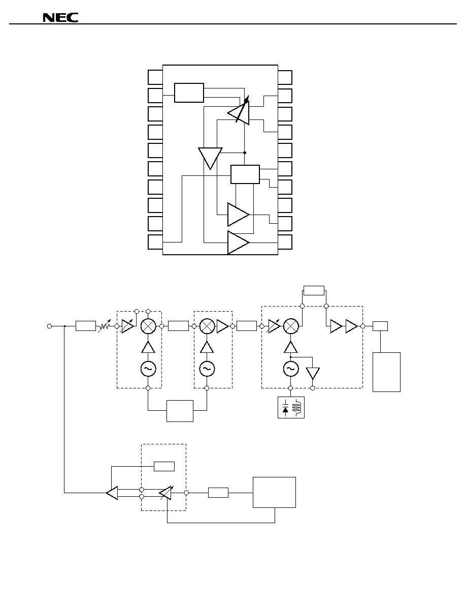
INTERNAL BLOCK DIAGRAM AND PIN CONFIGURATION (TOP VIEW)
1
2
3
4
5
6
7
8
9
10
BY2
VAGC
GND2A
GND2B
V
CC
1
V
CC
2
GND2C
GND2D
GND2E
BY3
BY1
AGC IN1
GND1A
AGC IN2
GND1B
PSAVE
PA_BIAS
GND3
OUT1
OUT2
20
19
18
17
16
15
14
13
12
11
Cont.
REG
TYPICAL APPLICATION
RF IN
50-750 MHz
RF Return
5-42 MHz
PC2799GR
µ
PC3211GR
Bias
LPF
Digital
QPSK
Modulator
DUAL
PLL
µ
PC1686GV
2nd IF
1st IF
µ
PC2798GR
Video Amplifier
QAM
Demo.
&FEC
DC-10 MHz
A/D
µ
HPF
SAW
SAW
LPF
Data Sheet P13564EJ3V0DS00
3
µ
µ
µ
µ
PC3211GR
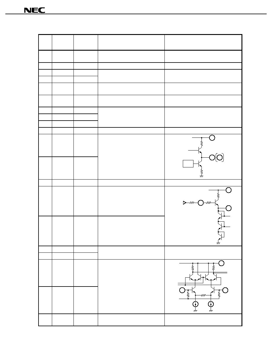
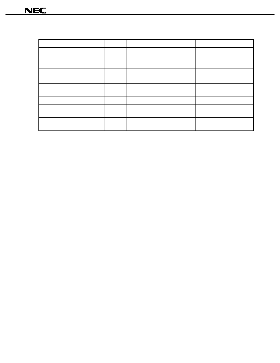
PIN FUNCTIONS
Pin
No.
Pin
Name
Pin
Voltage
TYP. (V)
Function and Explanation
Equivalent Circuit
1
BY2
≠
Non Connection pin.
This pin should be opened.
2
VAGC
0 to 3
Automatic gain control pin.
3
GND2A
0.0
4
GND2B
0.0
Ground pins of differential amplifier.
5
V
cc
1
9.0
Power supply pin of AGC amplifier
block.
6
V
cc
2
9.0
Power supply pin of differential
amplifier and output block.
7
GND2C
0.0
8
GND2D
0.0
9
GND2E
0.0
Ground pins of differential amplifier.
10
BY3
1.64
Bypass pin of regulator block.
11
OUT2
6.9
12
OUT1
6.9
Signal output pins.
This pins feature low-impedance
because of its emitter-follower output
port.
The pin that is not used should be
grounded through 50 ohm resistor.
6
REG
11
12
13
GND3
0.0
Ground pin of output block.
14
PA_BIAS
2.45
This is the pin to feed base bias in
case of connection to transistor as
power amplifier.
15
Psave
9.0
(+5 k
)
Power-save pin.
V
cc
: ON
GND : SLEEP
The 5 k
resistor should be
connected between 15 pin and V
cc
.
5
15
V
CC
(9 V)
5 k
14
16
GND1B
0.0
18
GND1A
0.0
Ground pin of AGC amplifier block.
17
AGC IN2
2.43
19
AGC IN1
2.43
Signal input pin.
In the case of single input, 17 or 19
pin should be grounded through
capacitor.
5
17
19
20
BY1
≠
Non Connection pin.
This pin should be opened.
Data Sheet P13564EJ3V0DS00
4
µ
µ
µ
µ
PC3211GR
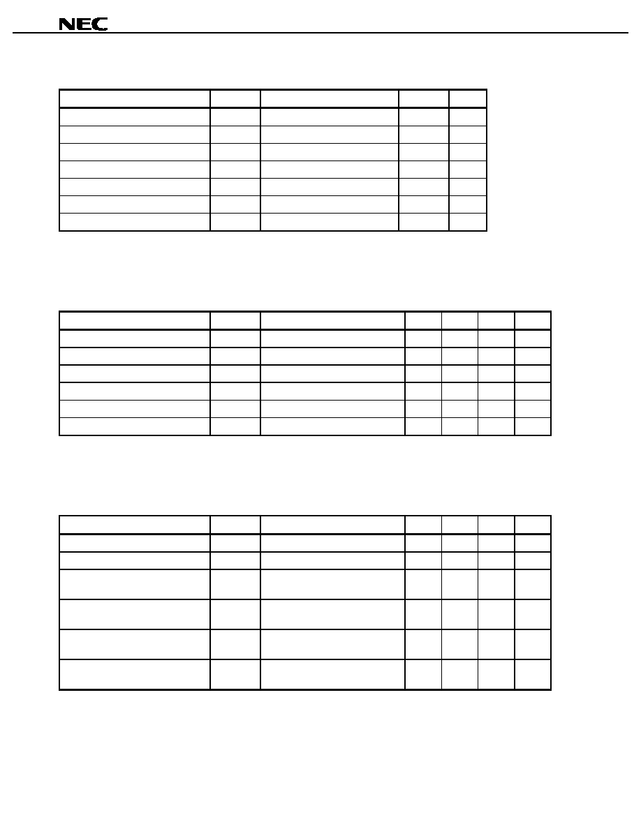
ABSOLUTE MAXIMUM RATINGS (T
A
= +25∞C unless otherwise specified)
Parameter
Symbol
Test Condition
Rating
Unit
Supply Voltage
V
CC
11.0
V
Power-save Voltage
V (Psave)
Note 1
11.0
V
AGC Voltage
V
AGC
3.6
V
Power Dissipation
P
D
T
A
= +75∞C
Note 2
500
mW
Operating Ambient Temperature
T
A
-
40 to +75
∞C
Storage Temperature
T
stg
-
55 to +150
∞C
Maximum Input Level
P
in
(MAX)
+5
dBm
Notes 1. Bias to 15 pin through 5 k
resistor.
2. Mounted on 50 mm
◊
50 mm
◊
1.6 mm double epoxy glass board.
RECOMMENDED OPERATING RANGE
Parameter
Symbol
Test Condition
MIN.
TYP.
MAX.
Unit
Supply Voltage
V
CC
8.0
9.0
10.0
V
Power-save Voltage
V (Psave)
Note
0
≠
10.0
V
AGC Control Voltage
V
AGC
0
≠
3.3
V
Operating Ambient Temperature
T
A
-
40
+25
+75
∞C
Input Frequency
f
in
5
≠
100
MHz
Maximum Input Level
P
in
(MAX)
≠
≠
0
dBm
Note Bias to 15 pin through 5 k
resistor.
ELECTRICAL CHARACTERISTICS (T
A
= +25∞C, V
CC
= 9 V, V
AGC
= 0 V, V (Psave) = 9 V (+5 k
), unless otherwise
specified)
Parameter
Symbol
Test Conditions
MIN.
TYP.
MAX.
Unit
Circuit Current 1
I
CC
1
No input signal
Note 1
29
38
51
mA
Maximum Gain
G
MAX
f
in
= 65 MHz, P
in
=
-
20 dBm Note 2
14
16
18
dB
Gain Control Range
GCR
f
in
= 65 MHz, P
in
=
-
20 dBm,
V
AGC
= 0 to 3 V
Note 2
47
55
≠
dB
Isolation at sleep mode
Isol
f
in
= 65 MHz, P
in
=
-
20 dBm,
V (Psave) = 0 V (+5 k
)
Note 2
60
65
≠
dB
2nd
order intermodulation distortion
IM
2
f
in
1 = 65 MHz, f
in
2 = 66.8 MHz,
P
out
=
-
10 dBm
Note 2
≠
≠44
≠40
dBc
3rd order intermodulation distortion
IM
3
f
in
1 = 65 MHz, f
in
2 = 66.8 MHz,
P
out
=
-
10 dBm
Note 2
≠
≠57
≠50
dBc
Notes 1. By measurement circuit 1
2. By measurement circuit 2
Data Sheet P13564EJ3V0DS00
5
µ
µ
µ
µ
PC3211GR
STANDARD CHARACTERISTICS (T
A
= +25∞C, V
CC
= 9 V, V
AGC
= 0 V, V (Psave) = 9 V (+5 k
), unless otherwise specified)
Parameter
Symbol
Test Conditions
Reference Value
Unit
Maximum Output Power
P
O (sat)
f
in
= 65 MHz, P
in
=
-
5 dBm
Note 1
+5
dBm
Circuit Current at Power-save mode
I
CC
(P/S)
No input signal, V (Psave) = 0 V (+5 k
)
Note 2
3
mA
Noise Figure
NF
f
in
= 65 MHz
Note 3
10
dB
Output Intercept Point
OIP
3
f
in
1 = 65 MHz, f
in
2 = 66.8 MHz Note 1
+16
dBm
Gain Flatness
G
flat
f
in
= 5 to 100 MHz, 6 MHz Band width
P
in
=
-
20 dBm
Note 1
±0.1
dB
Circuit Current 2
I
CC
2
No input signal, V
AGC
= 3 V
Note 2
43
mA
ON Time
t
ON
f
in
= 65 MHz,
V (Psave) = 0
9 V (+5 k
)
Note 4
200
µ
sec
OFF Time
t
OFF
f
in
= 65 MHz,
V (Psave) = 9
0 V (+5 k
)
Note 4
1.7
msec
Notes 1. By measurement circuit 2
2. By measurement circuit 1
3. By measurement circuit 3
4. By measurement circuit 4