 | –≠–ª–µ–∫—Ç—Ä–æ–Ω–Ω—ã–π –∫–æ–º–ø–æ–Ω–µ–Ω—Ç: UPC339C | –°–∫–∞—á–∞—Ç—å:  PDF PDF  ZIP ZIP |
©
1997
DATA SHEET
BIPOLAR ANALOG INTEGRATED CIRCUIT
µ
PC339
LOW POWER QUAD COMPARATOR
DESCRIPTION
The
µ
PC339 is a quad comparator which is designed
to operate from a single power supply over a wide range
of voltage. Operation from split power supplies, is also
possible and the power supply current drain is very low.
Further advantage, the input common-mode voltage in-
cludes ground, even though operated from a single power
supply voltage.
Document No. G11764EJ3V0DS00 (3rd edition)
(Previous No. IC-1986)
Date Published February 1997 N
Printed in Japan
FEATURES
∑
Common-mode input voltage range includes V
≠
∑
Wide supply voltage range
2 V to 32 V (Single)
±
1 V to
±
16 V (Split)
∑
Low supply current
∑
Open collector output
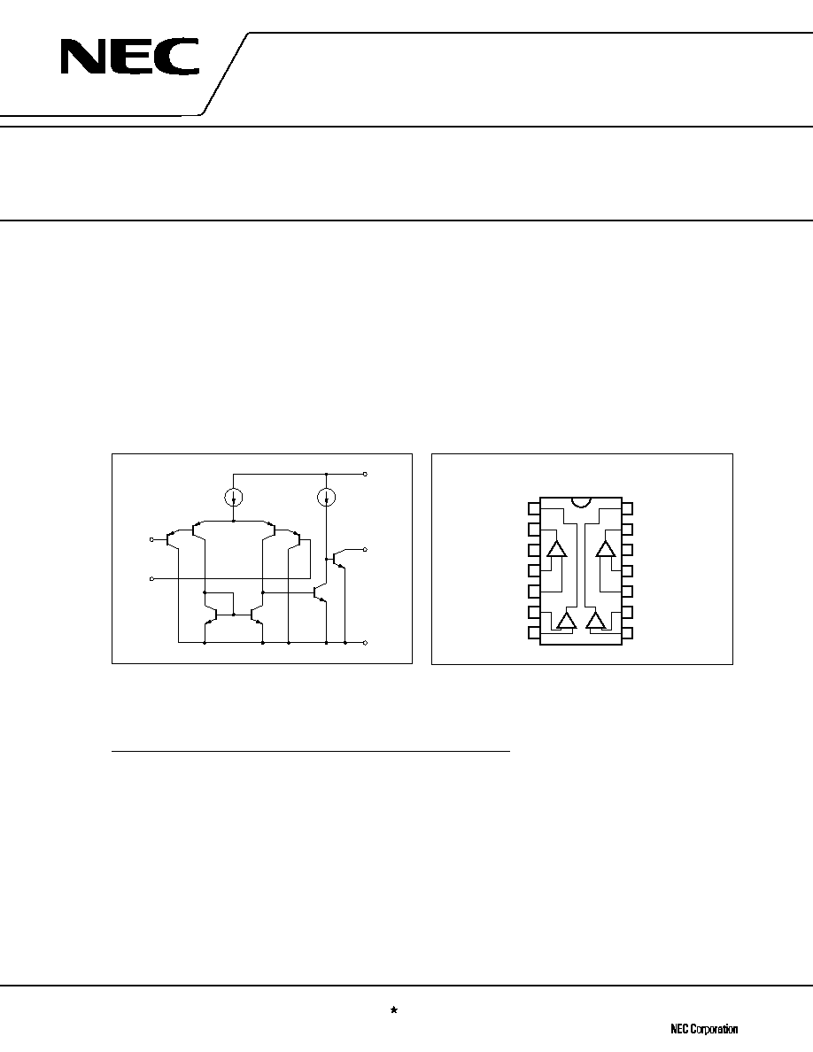
EQUIVALENT CIRCUIT (1/4 Circuit)
PIN CONFIGURATION (Top View)
The mark
shows major revised points.
The information in this document is subject to change without notice.
ORDERING INFORAMTION
Part Number
Package
µ
PC339C
14-pin plastic DIP (300 mil)
µ
PC339G2
14-pin plastic SOP (225 mil)
100 A
100 A
µ
µ
µ
V
+
V
≠
OUT
Q
8
Q
7
Q
6
Q
5
Q
2
Q
1
Q
3
Q
4
I
N
I
I
+
≠
1
2
3
4
5
6
7
14
13
12
11
10
9
8
OUT3
OUT4
V
≠
I
N4
I
I4
I
N3
I
I3
OUT2
OUT1
V
+
I
I1
I
N1
I
I2
I
N2
1
4
2
3
≠ +
≠ +
≠ +
≠ +
PC339C, 339G2
µ
PC339
2
ABSOLUTE MAXIMUM RATINGS (T
A
= 25
∞
C)
Parameter
Symbol
Ratings
Unit
Voltage between V
+
and V
≠
Note 1
V
+
≠V
≠
≠0.3 to +36
V
Differential Input Voltage
V
ID
±
36
V
Input Voltage
Note 2
V
I
V
≠
≠0.3 to V
≠
+36
V
Output Voltage
Note 3
V
O
V
≠
≠0.3 to V
≠
+36
V
Power Dissipation
C Package
Note 4
P
T
570
mW
G2 Package Note 5
550
mW
Output Short Circuit Duration
Note 6
Indefinite
sec
Operating Ambient Temperature
T
A
≠20 to +80
∞
C
Storage Temperature
T
stg
≠55 to + 125
∞
C
Notes 1. Reverse connection of supply voltage can cause destruction.
2. The input voltage should be allowed to input without damage or destruction independent of the
magnitude of V
+
. Either input signal should not be allowed to go negative by more than 0.3 V. The normal
operation will establish when any input is within the Common Mode Input Voltage Range of electrical
characteristics.
3. This specification is the voltage which should be allowed to supply to the output terminal from external
without damage or destruction independent of the magnitude of V
+
. Even during the transition period
of supply voltage, power on/off etc., this specification should be kept.
4. Thermal derating factor is ≠7.6 mW/
∞
C when operating ambient temperature is higher than 55
∞
C.
5. Thermal derating factor is ≠5.5 mW/
∞
C when operating ambient temperature is higher than 25
∞
C.
6. Short circuits from the output to V
+
can cause destruction. Pay careful attention to the total power
dissipation not to exceed the absolute maximum ratings, Note 4 and Note 5.
RECOMMENDED OPERATING CONDITIONS
Parameter
Symbol
MIN.
TYP.
MAX.
Unit
Supply Voltage (Split)
V
±
±
1
±
16
V
Supply Voltage (V
≠
= GND)
V
+
+2
+32
V
µ
PC339
3
ELECTRICAL CHARACTERISTICS (T
A
= 25
∞
C, V
+
= 5 V, V
≠
= GND)
Parameter
Symbol
Conditions
MIN.
TYP.
MAX.
Unit
Input Offset Voltage
V
IO
V
O
= 1.4 V, V
REF
= 1.4 V, R
S
= 0
±
2
±
5
mV
Input Offset Current
I
IO
V
O
= 1.4 V
±
5
±
50
nA
Input Bias Current
I
B
V
O
= 1.4 V
25
250
nA
Voltage Gain
A
V
R
L
= 15 k
200
V/mV
Supply Current
I
CC
R
L
=
, I
O
= 0 A, All Comparators
0.8
2
mA
Common Mode lnput Voltage Range
V
ICM
0
V
+
≠1.5
V
Output Saturation Voltage
V
OL
V
IN (≠)
= 1 V, V
IN (+)
= 0 V, I
O SINK
= 4 mA
0.2
0.4
V
Output Sink Current
I
O SINK
V
IN (≠)
= 1 V, V
IN (+)
= 0 V, V
O
1.5 V
6
16
mA
Output Leakage Current
I
O LEAK
V
IN (+)
= 1 V, V
IN (≠)
= 0 V, V
O
= 5 V
0.1
nA
Response Time
R
L
= 5.1 k
, V
RL
= 5 V
1.3
µ
s
∑
∑
∑
∑
µ
PC339
4
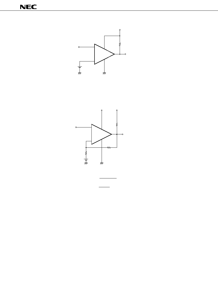
≠
+
R
L
OUT
1, 2
13, 14
12
3
V
IN
V
REF
4, 6, 8, 10
5, 7, 9, 11
V
+
V
REF
: V
≠
to V
+
≠1.5 (V)
V
+
V
RL
V
IN
R
1
R
2
V
REF
OUT
R
L
≠
+
COMPARATOR with HYSTERESIS CIRCUIT
APPLICATION CIRCUIT EXAMPLE
Threshold voltage
V
TH (High)
= V
REF
+ (V
RL
≠ V
REF
)
V
TH (Low)
= V
REF
≠ (V
REF
≠ V
OL
)
(V
RL
> V
REF
> V
OL
)
R
1
R
L
+ R
2
+ R
1
R
1
R
1
+ R
2
∑
∑
∑
∑
∑
µ
PC339
5
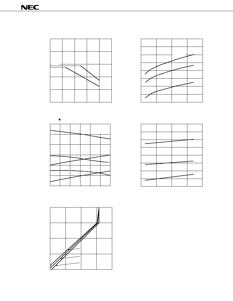
TYPICAL PERFORMANCE CHARACTERISTICS (T
A
= 25
∞
C, TYP.)
3
2
1
0
≠1
≠2
0
INPUT OFFSET VOLTAGE
40
20
≠40
≠20
≠3
60
80
V
+
= +5 V
V
≠
= GND
0
10
20
30
40
1.2
1.0
0.8
0.6
R
L
=
SUPPLY CURRENT
I
CC
- Supply Current - mA
T
A
= 25 ∞C
T
A
= 70 ∞C
T
A
= 0 ∞C
V
+
- Supply Voltage - V (V
≠
= GND)
1,000
800
600
400
200
0
20
40
60
80
100
339C
339G2
POWER DISSIPATION
T
A
- Operating Ambient Temperature - ∞C
T
A
- Operating Ambient Temperature - ∞C
P
T
- Total Power Dissipation - mW
V
IO
- Input Offset Voltage - mV
V
OL
- Output Saturation Voltage - V
50
40
30
20
10
0
10
20
30
40
I
B
- Input Bias Current - nA
T
A
= 0 ∞C
T
A
= 25 ∞C
T
A
= 70 ∞C
V
+
- Supply Voltage - V (V
≠
= GND)
INPUT BIAS CURRENT
10
1
0.1
0.01
0.001
0.01
0.1
1
10
100
T
A
= 70 ∞C
T
A
= 25 ∞C
T
A
= 0 ∞C
OUTPUT SATURATION VOLTAGE
I
O SINK
- Output Sink Current - mA