 | ÐлекÑÑоннÑй компоненÑ: UPC574J | СкаÑаÑÑ:  PDF PDF  ZIP ZIP |
Äîêóìåíòàöèÿ è îïèñàíèÿ www.docs.chipfind.ru
©
1998
DATA SHEET
BIPOLAR ANALOG INTEGRATED CIRCUIT
µ
PC574
MONOLITHIC BIPOLAR INTEGRATED CIRCUIT
VOLTAGE STABILIZER FOR ELECTRONIC TUNER
The
µ
PC574 is a monolithic integrated voltage stabilizer especially designed as voltage supplier for electronic
tuners.
FEATURES
·
Low temperature coefficient
·
Low dynamic resistance
·
Typical reference voltage of 33 V
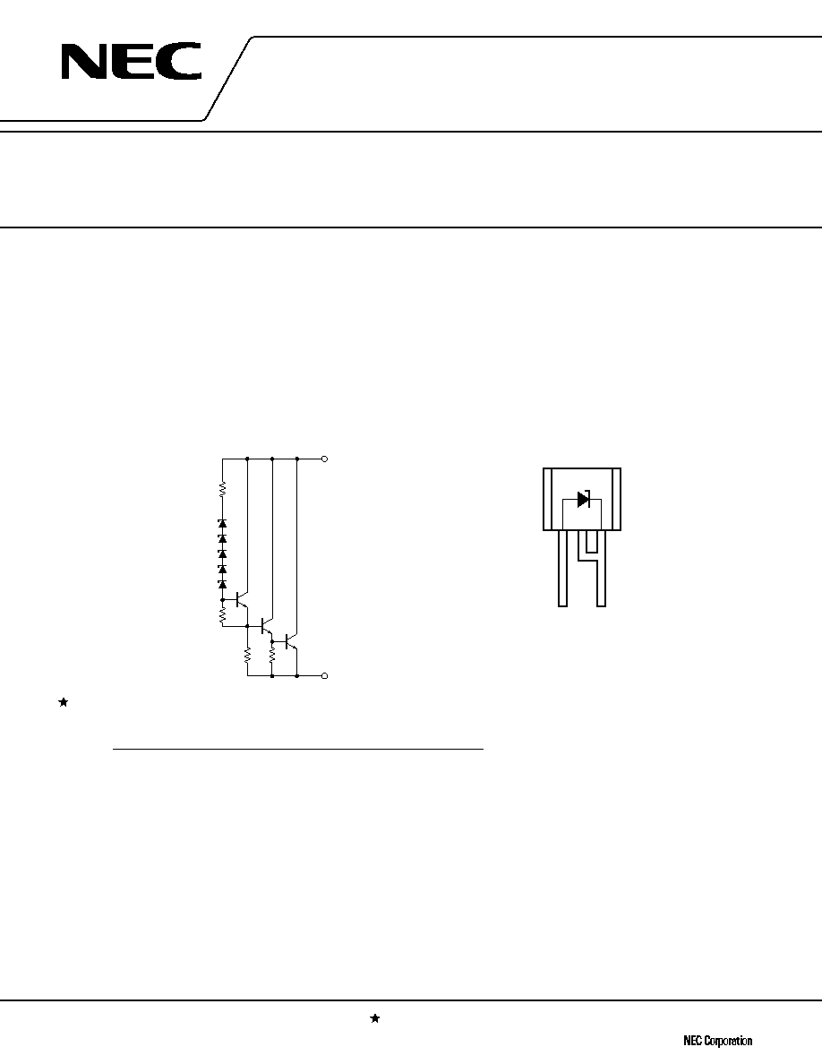
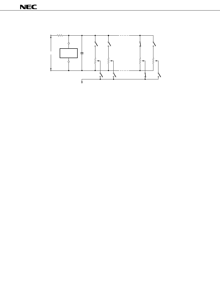
EQUIVALENT CIRCUIT
PIN CONFIGURATION (Marking Side)
µ
PC574J: 2-pin plastic SIP (TO-92)
ORDERING INFORMATION
Part Number
Package
µ
PC574J
2-pin plastic SIP (TO-92)
The information in this document is subject to change without notice.
The mark
shows major revised points.
Document No. S13200EJ4V0DS00 (4th edition)
(Previous No. IC-1006)
Date Published January 1998 N CP(K)
Printed in Japan
R
4
R
2
R
1
D
1
2
1
Q
3
Q
2
Q
1
D
2
D
3
D
4
D
5
R
3
2
1
1. Anode
2. Cathode
µ
PC574
2
ABSOLUTE MAXIMUM RATINGS (T
A
= 25
°
C, unless otherwise specified.)
Parameter
Symbol
Ratings
Unit
Zener Current
I
Z
10
mA
Power Dissipation
P
D
200 (T
A
= 75
°
C)
mW
Operating Ambient Temperature Range
T
A
20 to +75
°
C
Storage Temperature Range
T
stg
40 to +125
°
C
Caution Exposure to Absolute Maximum Ratings for extended periods may affect device reliability;
exceeding the ratings could cause permanent damage. The parameters apply independently. The
device should be operated within the limits specified under DC and AC Characteristics.
ELECTRICAL CHARACTERISTICS (T
A
= 25
°
C, unless otherwise specified.)
Parameter
Symbol
Conditions
MIN.
TYP.
MAX.
Unit
Stabilized Voltage
V
Z
I
Z
= 5 mA
31
35
V
Stabilized Voltage Temperature
V
Z
/
T
I
Z
= 5 mA, T
A
= 20 to +75
°
C
1.0
0
+1.0
mV/
°
C
Drift
Dynamic Resistance
r
Z
I
Z
= 5 mA, f = 1 kHz, I
AC
= 0.5 mA
10
25
µ
PC574
3
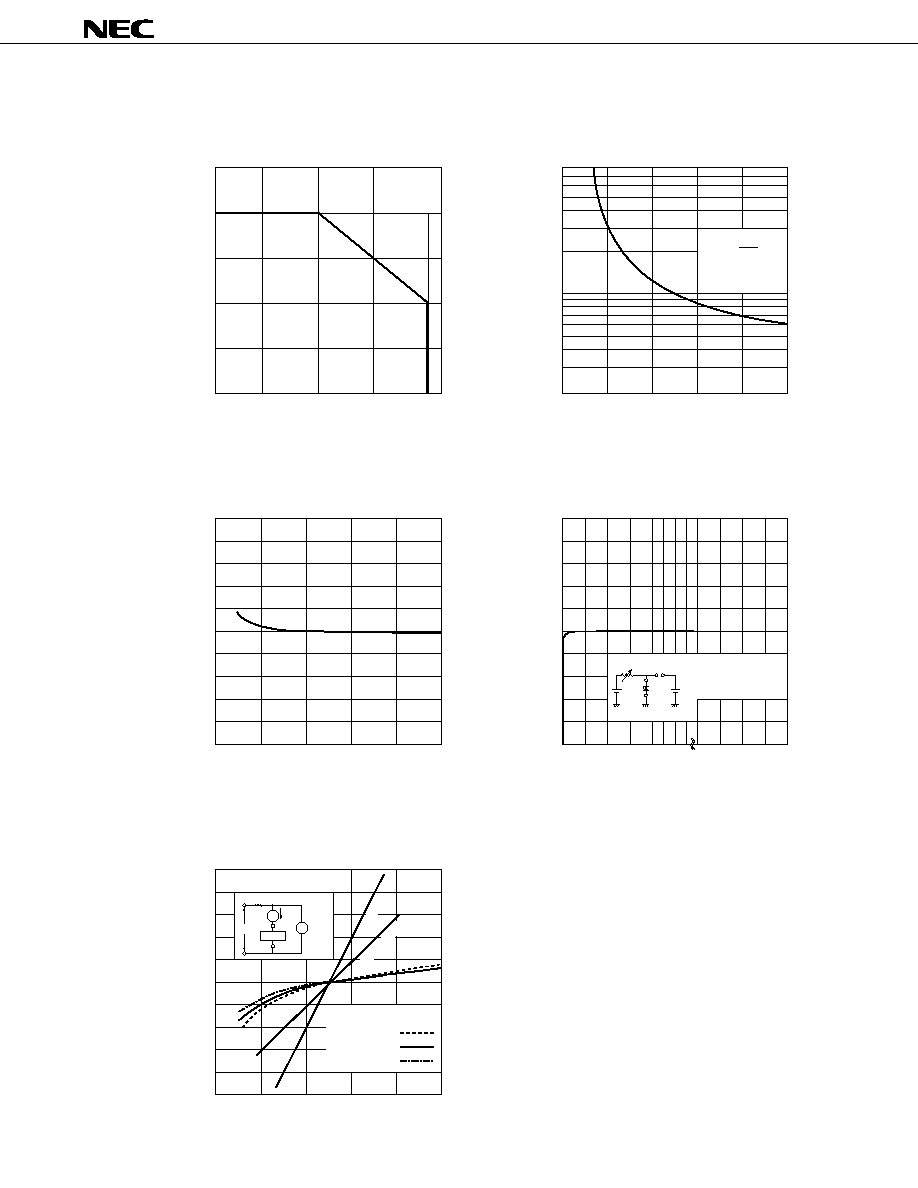
TYPICAL CHARACTERISTIC (T
A
= 25
°
C, unless otherwise specified.)
P
D
- Power Dissipation - mW
Power Dissipation vs.
Ambient Temperature
Free Air
400
300
200
100
80
+80
+60
+40
+20
0
20
40
60
80
0
5
10 15 20304050 1
5
10 20 30
60
40
20
10
8
6
4
2
0
2
4
6
8
10
T
A
- Operating Ambient Temperature - °C
V
Z
/ T - Stabilized Voltage Temperature Drift - mV/°C
Stabilized Voltage Temperature
Drift vs. Zener Current
I
Z
- Zener Current - mA
( V
Z
/V
Z
)
×
100 - Stabilized Voltage Variation - %
V
B
- Supply Voltage Variation - V
Stabilized Voltage Variation &
Supply Voltage Variation vs.
Zener Current
I
Z
- Zener Current - mA
r
Z
- Dynamic Resistance -
Dynamic Resistance vs.
Zener Current
I
Z
- Zener Current - mA
V
Z
- Stabilized Voltage Variation - mV
Stabilized Voltage Variation
vs. Time
t - Time
s.
min.
I
AC
=
f = 1 kHz
I
Z
10
+4
20
0
25
50
75
+3
+2
+1
0
1
2
3
4
+1.0
+0.8
+0.6
+0.4
+0.2
0
0.2
0.4
0.6
0.8
1.0
+30
+20
+10
0
10
20
30
0
2
4
6
8
10
0
2
4
6
8
10
+
V
REF
I
Z
= 5 mA XY Recoder
Free Air
I
Z
= 5 mA
V
Z
= 33.11 V
A
2
V
Z
R
S
I
Z
1
574J
V
B
V
R
S
= 20 k
R
S
= 10 k
Reference I
Z
= 5 mA
V
Z
= V
Z
(I
Z
) V
Z
(5)
T
A
= 20 °C
T
A
= +25 °C
T
A
= +75 °C
µ
PC574
4
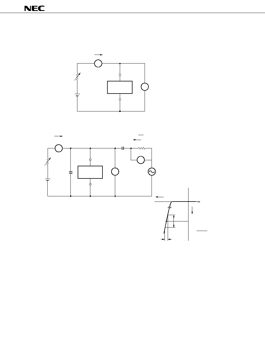
MEASURING CIRCUITS
(i) Measuring Circuit for Stabilized Voltage V
Z
Digital Volt Meter
R
B
E
B
I
Z
= 5 mA
A
V
2
1
PC574
µ
(ii) Measuring Circuit for Dynamic Resistance r
Z
I
Z
V
Z
I
Z
0.5 mA
5 mA
f = 1 kHz
100
50 F
µ
R
B
E
B
A
VV
1
VV
2
2
+
C
0.1 F
µ
1
PC574
µ
I
AC
=
I
Z
10
r
Z
=
VV
1
0.5 mA
VV
1
µ
PC574
5
TYPICAL APPLICATION
2
Ach
R
i
V
i
Bch
Ych
Zch
C
15 k
15 k
15 k
15 k
Channel setting
Variable resistor
in case of Ych ON
to tuning diodes (VARACTOR)
1
PC574
µ
µ
PC574
6
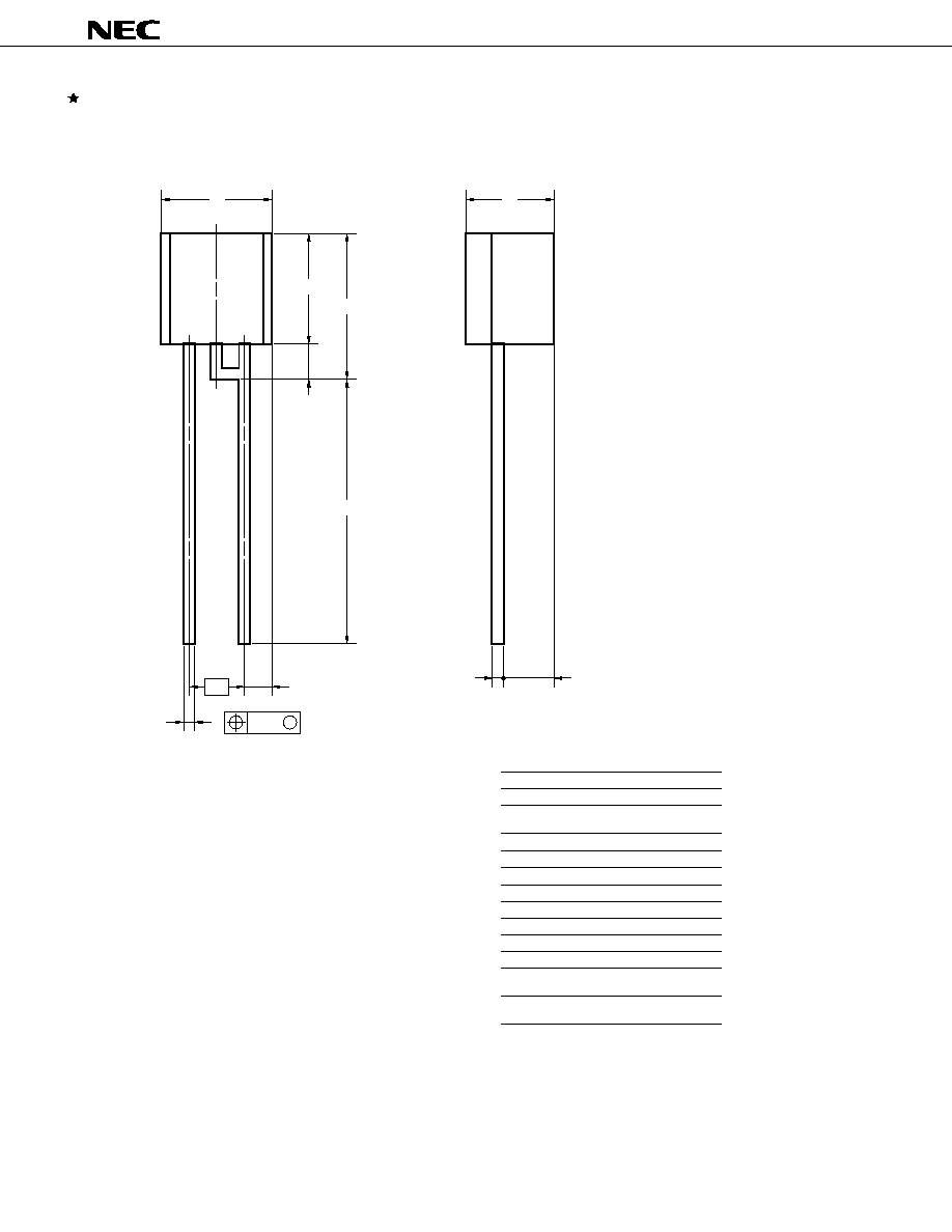
PACKAGE DRAWING
F
G
M
1
2
J
U
V
A
N
M
K
Q
Y
H
NOTE
Each lead centerline is located within 0.25 mm (0.01 inch) of
its true position (T.P.) at maximum material condition.
P2J-254B-1
ITEM
MILLIMETERS
INCHES
A
F
G
H
J
K
M
N
Q
U
5.2 MAX.
0.25
1.8 MIN.
5.5 MAX.
4.2 MAX.
0.5±0.1
V
Y
15.0±0.7
2.8 MAX.
8.0 MAX.
0.5±0.1
2.54
1.33 MAX.
0.205 MAX.
0.02
0.1
0.053 MAX.
0.07 MIN.
0.217 MAX.
0.166 MAX.
0.315 MAX.
0.111 MAX.
0.02
0.591
+0.028
0.029
0.01
+0.004
0.005
+0.004
0.005
2 PIN PLASTIC SIP (TO-92)
µ
PC574
7
RECOMMENDED SOLDERING CONDITIONS
When soldering this product, it is highly recommended to observe the conditions as shown below. If other soldering
processes are used, or if the soldering is performed under different conditions, please make sure to consult with our
sales offices.
For more details, refer to our document "SEMICONDUCTOR DEVICE MOUNTING TECHNOLOGY MANUAL"
(C10535E).
Through-hole device
µ
PC574J: 2-pin plastic SIP (TO-92)
Process
Conditions
Wave soldering
Solder temperature: 260
°
C or below,
(only to leads)
Flow time: 10 seconds or less.
Partial heating method
Pin temperature: 300
°
C or below,
Heat time: 3 seconds or less (per each lead.)
Caution For through-hole device, the wave soldering process must be applied only to leads, and make
sure that the package body does not get jet soldered.

µ
PC574
No part of this document may be copied or reproduced in any form or by any means without the prior written
consent of NEC Corporation. NEC Corporation assumes no responsibility for any errors which may appear in
this document.
NEC Corporation does not assume any liability for infringement of patents, copyrights or other intellectual property
rights of third parties by or arising from use of a device described herein or any other liability arising from use
of such device. No license, either express, implied or otherwise, is granted under any patents, copyrights or other
intellectual property rights of NEC Corporation or others.
While NEC Corporation has been making continuous effort to enhance the reliability of its semiconductor devices,
the possibility of defects cannot be eliminated entirely. To minimize risks of damage or injury to persons or
property arising from a defect in an NEC semiconductor device, customers must incorporate sufficient safety
measures in its design, such as redundancy, fire-containment, and anti-failure features.
NEC devices are classified into the following three quality grades:
"Standard", "Special", and "Specific". The Specific quality grade applies only to devices developed based on a
customer designated "quality assurance program" for a specific application. The recommended applications of
a device depend on its quality grade, as indicated below. Customers must check the quality grade of each device
before using it in a particular application.
Standard: Computers, office equipment, communications equipment, test and measurement equipment,
audio and visual equipment, home electronic appliances, machine tools, personal electronic
equipment and industrial robots
Special:
Transportation equipment (automobiles, trains, ships, etc.), traffic control systems, anti-disaster
systems, anti-crime systems, safety equipment and medical equipment (not specifically designed
for life support)
Specific:
Aircrafts, aerospace equipment, submersible repeaters, nuclear reactor control systems, life
support systems or medical equipment for life support, etc.
The quality grade of NEC devices is "Standard" unless otherwise specified in NEC's Data Sheets or Data Books.
If customers intend to use NEC devices for applications other than those specified for Standard quality grade,
they should contact an NEC sales representative in advance.
Anti-radioactive design is not implemented in this product.
M4 96.5
[MEMO]
The application circuits and their parameters are for reference only and are not intended for use in actual design-ins.
Document Outline