The information in this document is subject to change without notice. Before using this document, please
confirm that this is the latest version.
BIPOLAR ANALOG INTEGRATED CIRCUITS
µ
µ
µ
µ
PC8119T,
µ
µ
µ
µ
PC8120T
VARIABLE GAIN AMPLIFIER SILICON MMIC
FOR TRANSMITTER AGC OF DIGITAL CELLULAR TELEPHONE
1996
©
Document No. P11027EJ2V0DS00 (2nd edition)
Date Published October 1998 N CP(K)
Printed in Japan
DATA SHEET
The mark shows major revised points.
DESCRIPTION
The
µ
PC8119T and
µ
PC8120T are silicon monolithic integrated circuits designed as variable gain amplifier. Due to
100 MHz to 1.9 GHz operation, these ICs are suitable for RF transmitter AGC stage of digital cellular telephone. Two
types of gain control let users choose in accordance with system design. 3 V supply voltage and mini mold package
contribute to make system lower voltage, decreased space and fewer components.
The
µ
PC8119T and
µ
PC8120T are manufactured using NEC's 20 GHz f
T
NESAT
TM
III silicon bipolar process. This
process uses silicon nitride passivation film and gold electrodes. These materials can protect chip surface from external
pollution and prevent corrosion / migration. Thus, this IC has excellent performance, uniformity and reliability.
FEATURES
∑
Recommended operating frequency : f = 100 MHz to 1.92 GHz
∑
Supply voltage
: V
CC
= 2.7 to 3.3 V
∑
Low current consumption
: I
CC
= 11 mA
TYP
.
@ V
CC
= 3.0 V
∑
Gain control voltage
: V
AGC
= 0.6 to 2.4 V (recommended)
∑
Two types of gain control
:
µ
PC8119T = V
AGC
up vs. Gain down
(Forward control)
µ
PC8120T = V
AGC
up vs. Gain up
(Reverse control)
∑
AGC control can be constructed by external control circuit.
∑
High-density surface mounting
APPLICATIONS
∑
1.9 GHz cordless telephone (PHS base-station and so on)
∑
800 MHz to 900 MHz or 1.5 GHz Digital cellular telephone (PDC800M, PDC1.5G and so on)
ORDERING INFORMATION
Part Number
Package
Marking
Supplying Form
Gain Control Type
µ
PC8119T-E3
C2M
Forward control
µ
PC8120T-E3
6-pin minimold
C2N
Embossed tape 8 mm wide.
1, 2, 3 pins face to perforation side of the tape.
Qty 3 kp/reel.
Reverse control
Remark
To order evaluation samples, please contact your local NEC sales office.
(Part number for sample order:
µ
PC8119T,
µ
PC8120T)
Caution
Electro-static sensitive devices
2
µ
µ
µ
µ
PC8119T,
µ
µ
µ
µ
PC8120T
PIN CONNECTIONS
Pin No.
Pin Name
1
INPUT
2
GND
3
GND
4
OUTPUT
5
V
CC
6
V
AGC
(Top View)
Marking is a example for PC8119T.
C2M
3
2
1
4
5
6
(Bottom View)
4
5
6
3
2
1
µ
VARIABLE GAIN AMPLIFIER PRODUCT LINE-UP
Part No.
V
CC
(V)
I
CC
(mA)
V
AGC
(V)
V
AGC
up vs.Gain
f (GHz)
P
O (1 dB)
Features
µ
PC2723T
4.5 to 5.5
15
3.3 to 5.0
down
up to 1.1
≠4
µ
PC8119T
2.7 to 3.3
11
0.6 to 2.4
down
0.1 to 1.92
+3
Excellent V
CC
fluctuation
µ
PC8120T
2.7 to 3.3
11
0.6 to 2.4
up
0.1 to 1.92
+3
µ
PC8130TA
2.7 to 3.3
11
0.6 to 2.4
up
0.8 to 1.5
+5
Low distortion
µ
PC8131TA
2.7 to 3.3
11
0 to 2.4
down
0.8 to 1.5
+5
Low distortion
Remark
Typical performance. Please refer to ELECTRICAL CHARACTERISTICS in detail.
To know the associated product, please refer to each latest data sheet.
SYSTEM APPLICATION EXAMPLE
SW
˜
N
PLL
PLL
I
Q
DEMO
I
Q
0
∞
PC8119T
or
PC8120T
PA
TX
RX
LNA
90
∞
µ
µ
3
µ
µ
µ
µ
PC8119T,
µ
µ
µ
µ
PC8120T
PIN EXPLANATION
Pin
No.
Pin Name
Applied
Voltage
V
Pin
Voltage
V
Note
Function and Applications
Internal Equivalent Circuit
1
IN
≠
1.2
RF input pin. This pin should be
coupled with capacitor (eg 1000
pF) for DC cut. This pin can be
input from 50
impedance signal
source without matching circuit.
2
3
GND
0
≠
Ground pin. This pin should be
connected to system ground with
minimum inductance. Ground
pattern on the board should be
formed as wide as possible.
4
OUT
Voltage
as same
as V
CC
through
external
inductor
≠
RF output pin. This pin is
designed as open collector of
high impedance.
This pin must be externally
equipped with matching circuits.
1
2
3
5
4
Bias
circuit
Control
circuit
5
V
CC
2.7 to 3.3
≠
Supply voltage pin. This pin must
be externally equipped with low
pass filter (eg
type) in order to
suppress leakage from input pin.
This pin also must be equipped
with bypass capacitor (eg 1000
pF) to minimize ground
impedance.
Gain control pin. The relation
between product number and
control performance is shown
below;
Part No.
V
AGC
up vs. Gain
µ
PC8119T
down
µ
PC8120T
up
6
V
AGC
0 to 3.3
≠
Control
circuit
2
3
5
6
Note Pin voltage is measured at V
CC
= 3.0 V.
4
µ
µ
µ
µ
PC8119T,
µ
µ
µ
µ
PC8120T
ABSOLUTE MAXIMUM RATINGS
Parameter
Symbol
Conditions
Ratings
Unit
Supply Voltage
V
CC
T
A
= +25∞C
3.6
V
Gain Control Voltage
V
AGC
T
A
= +25∞C
3.6
mA
Operating Ambient
Temperature
T
A
-
40 to +85
∞C
Storage Temperature
T
stg
≠55 to +150
∞C
Power Dissipation of
Package
P
D
Mounted on double-sided copper-clad 50
◊
50
◊
1.6
mm epoxy glass PWB
T
A
= +85∞C
280
mW
RECOMMENDED OPERATING CONDITIONS
Parameter
Symbol
MIN.
TYP.
MAX.
Unit
Notice
Supply Voltage
V
CC
2.7
3.0
3.3
V
Same voltage should be applied to 4 and 5
pins.
Gain Control Voltage
V
AGC
0.6
≠
2.4
V
I
AGC
0.1 mA
≠
≠
≠18
P
adj
≠60 dBc @
f =
±
50 kHz
Note 1
Input Level
P
in
≠
≠
≠10
dBm
P
adj
≠60 dBc @
f =
±
600 kHz
Note 2
Operating Ambient
Temperature
T
A
≠40
+25
+85
∞C
Operating Frequency
f
100
≠
1920
MHz
With external output-matching
AGC Pin Drive Current
I
AGC
0.5
≠
≠
mA
V
AGC
3.3 V
Notes 1. Adjacent Channel Interference (P
adj
) wave form condition: f = 950 MHz or 1440 MHz,
/4QPSK
modulation signal, data rate = 42 kbps, rolloff ratio = 0.5, PN9 bits (pseudo random pattern)
2. Adjacent Channel Interference (P
adj
) wave form condition: f = 1900 MHz,
/4QPSK modulation signal,
data rate = 384 kbps, rolloff ratio = 0.5, PN9 bits (pseudo random pattern)
5
µ
µ
µ
µ
PC8119T,
µ
µ
µ
µ
PC8120T
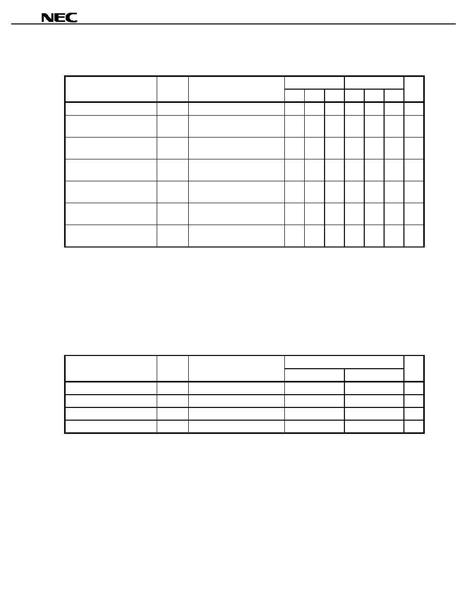
ELECTRICAL CHARACTERISTICS
(Unless otherwise specified, T
A
= +25∞C, V
CC
= V
out
= 3.0 V, Z
S
= Z
L
= 50
, External matched output port)
µ
PC8119T
µ
PC8120T
Parameter
Symbol
Test Conditions
MIN.
TYP.
MAX.
MIN.
TYP.
MAX.
Unit
Circuit Current
I
CC
No signal, I
CC
= I
VCC
+ I
out
7.5
11
15
7.5
11
15
mA
Maximum Power Gain
G
PMAX
f = 950 MHz, P
in
= ≠30 dBm
f = 1440 MHz, P
in
= ≠30 dBm
10
10
12.5
13
15
16
10.5
10.5
13
13.5
15.5
16.5
dB
Gain Control Range
Note
GCR
f = 950 MHz, Pin = ≠30 dBm
f = 1440 MHz, Pin = ≠30 dBm
40
35
50
45
≠
≠
40
35
50
45
≠
dB
Noise Figure
NF
f = 950 MHz, G
PMAX
f = 1440 MHz, G
PMAX
≠
≠
8.5
7.5
11.5
10.5
≠
≠
9.0
7.5
12
10.5
dB
Isolation
ISL
f = 950 MHz, G
PMAX
f = 1440 MHz, G
PMAX
27
31
32
36
≠
≠
26
30
31
35
≠
≠
dB
Input Return Loss
RL
in
f = 950 MHz, G
PMAX
f = 1440 MHz, G
PMAX
3
3
6
6
≠
≠
3
3
6
6
≠
≠
dB
1 dB Compression Output
Power
P
O (1 dB)
f = 950 MHz, G
PMAX
f = 1440 MHz, G
PMAX
0
+1.0
+3
+4
≠
≠
+0.5
0
+3.5
+3
≠
≠
dBm
Note Gain Control Range (GCR) specification: GCR = G
PMAX
≠ G
PMIN
(dB)
Conditions
µ
PC8119T: G
PMAX
@ V
AGC
= 0 V, G
PMIN
@ V
AGC
= V
CC
µ
PC8120T: G
PMAX
@ V
AGC
= V
CC
, G
PMIN
@ V
AGC
= 0 V
Remark
Measured on TEST CIRCUIT 1 and 2
STANDARD CHARACTERISTICS FOR REFERENCE
(Unless otherwise specified, T
A
= +25∞C, V
CC
= V
out
= 3.0 V, Z
S
= Z
L
= 50
, External matched output port)
Reference Value
Parameter
Symbol
Test Conditions
µ
PC8119T
µ
PC8120T
Unit
Maximum Power Gain
G
PMAX
f = 1900 MHz, P
in
= ≠30 dBm
12.5
13
dB
Gain Control Range
Note
GCR
f = 1900 MHz, P
in
= ≠30 dBm
22
22
dB
Noise Figure
NF
f = 1900 MHz, G
PMAX
7.2
7.3
dB
1 dB Compression Output Power
P
O (1 dB)
f = 1900 MHz, G
PMAX
+3.0
+2.5
dBm
Note Gain Control Range (GCR) specification: GCR = G
PMAX
≠ G
PMIN
(dB)
Conditions
µ
PC8119T: G
PMAX
@ V
AGC
= 0 V, G
PMIN
@ V
AGC
= V
CC
µ
PC8120T: G
PMAX
@ V
AGC
= V
CC
, G
PMIN
@ V
AGC
= 0 V
Remark
Measured on APPLICATION CIRCUIT EXAMPLE