FEATURES
SILICON MMIC LOW
CURRENT AMPLIFIER
FOR MOBILE COMMUNICATIONS
∑ HIGH DENSITY SURFACE MOUNTING:
6 Pin Leadless Minimold Package (1.5 x 1.1 x 0.55 mm)
∑ SUPPLY VOLTAGE:
V
CC
= 2.4 to 3.3 V
∑ HIGH EFFICIENCY:
P
O
(1dB) = +2.0 dBm TYP at f = 1.0 GHz
P
O
(1dB) = +0.5 dBm TYP at f = 1.9 GHz
P
O
(1dB) = +0.5 dBm TYP at f = 2.4 GHz
∑ POWER GAIN:
G
P
= 13.5 dB TYP at f = 1.0 GHz
G
P
= 15.5 dB TYP at f = 1.9 GHz
G
P
= 16.0 dB TYP at f = 2.4 GHz
∑ EXCELLENT ISOLATION:
ISL = 43 dB TYP at f = 1.0 GHz
ISL = 42 dB TYP at f = 1.9 GHz
ISL = 42 dB TYP at f = 2.4 GHz
∑ LOW CURRENT CONSUMPTION:
I
CC
= 4.0 mA TYP AT VCC = 3.0 V
∑ OPERATING FREQUENCY:
0.1 to 2.4 GHz (Output port LC matching)
∑ LIGHT WEIGHT:
3 mg
UPC8179TK
California Eastern Laboratories
∑ Buffer amplifiers for 0.1 to 2.4 GHz mobile communications
systems.
APPLICATION
PART NUMBER
UPC8179TK
PACKAGE OUTLINE
TK
SYMBOLS
PARAMETERS AND CONDITIONS
UNITS
MIN
TYP
MAX
I
CC
Circuit Current (no input signal)
mA
2.9
4.0
5.4
GP
Power Gain,
f = 1.0 GHz, P
IN
= -30 dBm
dB
11.0
13.5
15.5
f = 1.9 GHz, P
IN
= -30 dBm
13.0
15.5
17.5
f = 2.4 GHz, P
IN
= -30 dBm
14.0
16.0
18.5
ISOL
Isolation,
f = 1.0 GHz, P
IN
= -30 dBm
dB
39.0
43.0
≠
f = 1.9 GHz, P
IN
= -30 dBm
37.0
42.0
≠
f = 2.4 GHz, P
IN
= -30 dBm
37.0
42.0
≠
P
1dB
Output Power at
f = 1.0 GHz
dBm
-0.5
2.0
≠
1 dB gain
f = 1.9 GHz
-2.0
0.5
≠
compression,
f = 2.4 GHz
-3.0
0.5
≠
NF
Noise Figure,
f = 1.0 GHz
dB
≠
5.0
6.5
f = 1.9 GHz
≠
5.0
6.5
f = 2.4 GHz
≠
5.0
6.5
RL
IN
Input Return Loss,
f = 1.0 GHz, P
IN
= -30 dBm
dB
4.0
7.0
≠
(without matching
f = 1.9 GHz, P
IN
= -30 dBm
4.0
7.0
≠
circuit)
f = 2.4 GHz, P
IN
= -30 dBm
6.0
9.0
≠
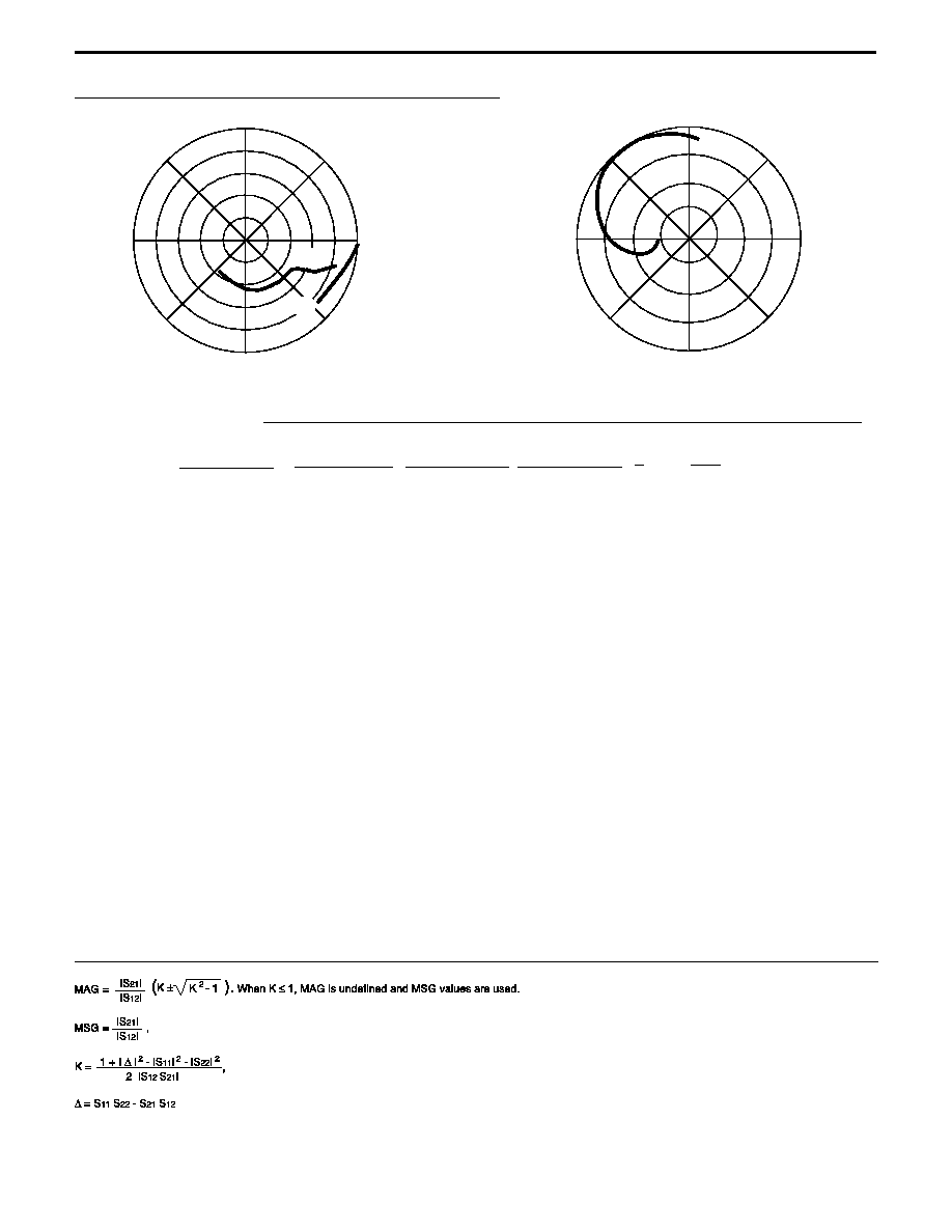
ELECTRICAL CHARACTERISTICS,
(Unless otherwise specified, T
A
= +25
∞
C, V
CC
= V
OUT
= 3.0 V, Z
S
= Z
L
= 50
, at LC matched Frequency)
NEC's UPC8179TK is a silicon monolithic integrated circuit
designed as an amplifier for mobile communications. This IC
can realize low current consumption with external chip induc-
tor. The incorporation of a chip identical to the conventional 6-
pin super minimold package (2.0 x 1.25 x 0.9 mm)
µ
PC8179TB
in a 6-pin leadless minimold package (1.5 x 1.1 x 0.55 mm) has
enabled a reduction in mounting area of 50 %. The
µ
PC8179TK
is ideally suited to replace the
µ
PC8179TB for footprint reduc-
tion and increased design density. This IC is manufactured
using NEC's 30 GHz fMAX UHS0 (Ultra High Speed Process)
silicon bipolar process. This process uses direct silicon nitride
passivation film and gold electrodes. These materials can
protect the chip surface from pollution and prevent corrosion/
migration. Thus this IC has excellent performance uniformity
and reliability.
NEC's stringent quality assurance and test procedures assure
the highest performance. consistency and reliability.
DESCRIPTION
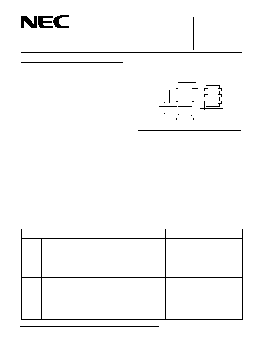
OUTLINE DIMENSIONS
(Units in mm)
PACKAGE OUTLINE TK
0.2±0.1
(0.9)
0.11±
+0.1
-0.05
0.55±0.03
0.96
1.5±0.1
0.16±0.05
1.3±0.05
0.48
0.48
0.1
1.1±0.1
Top
View
Bottom
View
UPC8179TK
ABSOLUTE MAXIMUM RATINGS
1
(T
A
= 25
∞
C)
SYMBOLS
PARAMETERS
UNITS
RATINGS
V
CC
Supply Voltage
V
3.6
I
CC
Circuit Current
mA
15
P
D
Power Dissipation
2
mW
232
T
OP
Operating Temperature
∞
C
-40 to +85
T
STG
Storage Temperature
∞
C
-55 to +150
P
IN
Input Power
dBm
+5
SYMBOLS
PARAMETERS
UNITS MIN
TYP MAX
V
CC
Supply Voltage
V
2.4
3.0
3.3
T
A
Operating Ambient
∞
C
-40
+25
+85
Temperature
RECOMMENDED
OPERATING CONDITIONS
Notes:
1. Operation in excess of any one of these parameters may result
in permanent damage.
2. Mounted on a 50 x 50 x 1.6 mm epoxy glass PWB (T
A
= +85
∞
C).
Parameter
1.0 GHz output port
1.9 GHz output port
2.4 GHz output port
Package
matching frequency
matching frequency
matching frequency
I
CC
G
P
ISOL
P
O(1 dB)
G
P
ISOL
P
O(1 dB)
G
P
ISOL
P
O(1 dB)
Part No.
(mA)
(dB)
(dB)
(dBm)
(dB)
(dB)
(dBm)
(dB)
(dB)
(dBm)
UPC8178TB
1.9
11
39
-4.0
11.5
40
-7.0
11.5
38
-7.5
6 pin super minimold
UPC8178TK
1.9
11
40
-5.5
11.0
41
-8.0
11.0
42
-8.0
6 pin leadless minimold
UPC8179TB
4.0
13.5
44
+3.0
15.5
42
+1.5
15.5
41
+1.0
6 pin super minimold
UPC8179TK
4.0
13.5
43
+2.0
15.5
42
+0.5
16.0
42
+0.5
6 pin leadless minimold
UPC8128TB
2.8
12.5
39
-4.0
13
37
-4.0
≠
≠
≠
6 pin super minimold
UPC8151TB
4.2
12.5
38
+2.5
15
34
+0.5
≠
≠
≠
6 pin super minimold
UPC8152TB
5.6
23
40
-4.5
17.5
35
-8.5
≠
≠
≠
6 pin super minimold
SERIES PRODUCTS
1
(T
A
= +25
∞
C, V
CC
= V
out
= 3.0 V, Z
S
= Z
L
= 50
)
Note:
1. Typical performance.
PIN CONNECTIONS
PIN NO.
PIN NAME
1
INPUT
2
GND
3
GND
4
OUTPUT
5
GND
6
V
CC
Caution: pin arrangement differs from the conventional 6 pin super minimold type UPC8179TB ≠
4
5
6
4
5
6
1
2
3
1
2
3
6C
(Top View)
(Bottom View)
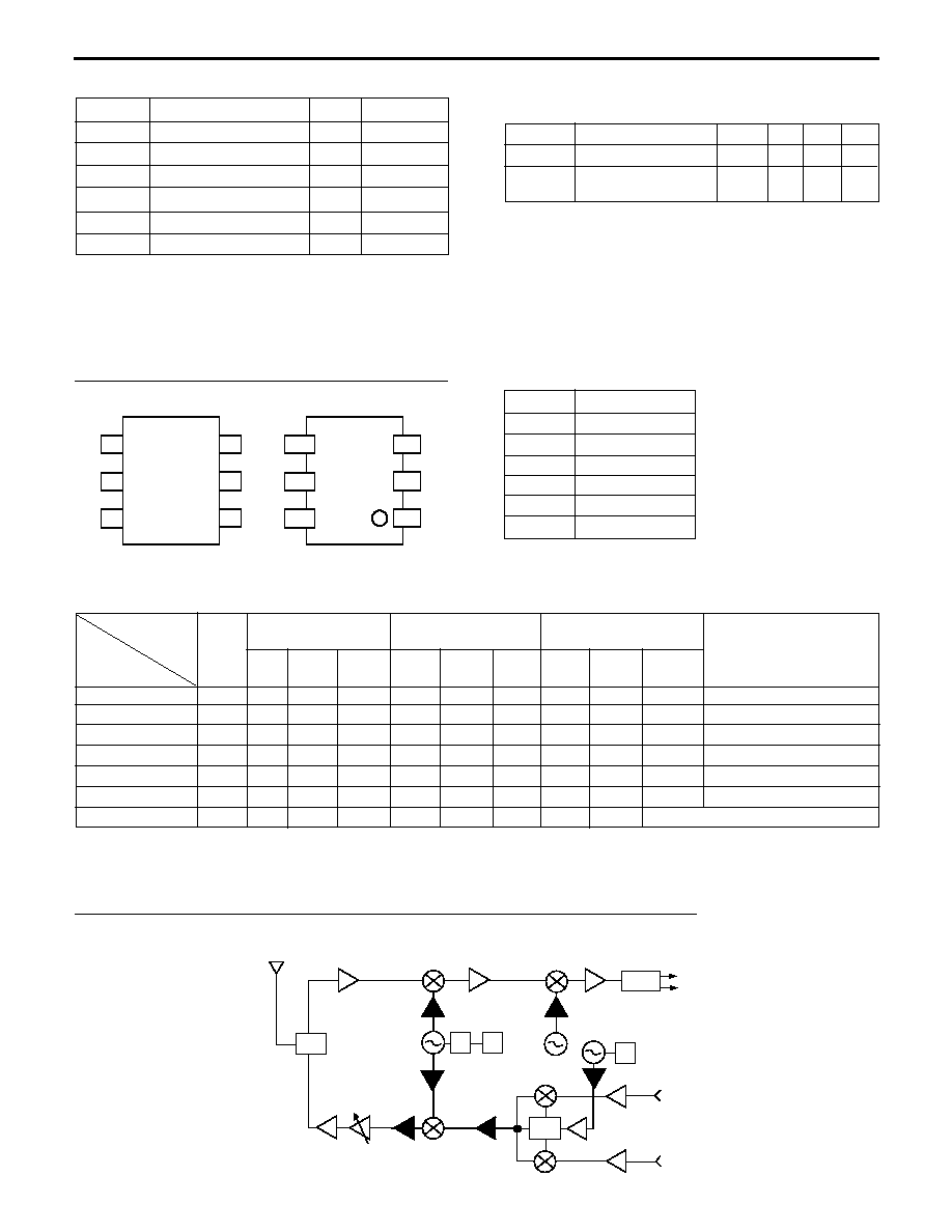
SYSTEM APPLICATION EXAMPLE
Location examples in digital cellular
I
Q
0∞
90∞
DEMOD
Q
˜N
PLL
PLL
I
RX
TX
PA
LNA
SW
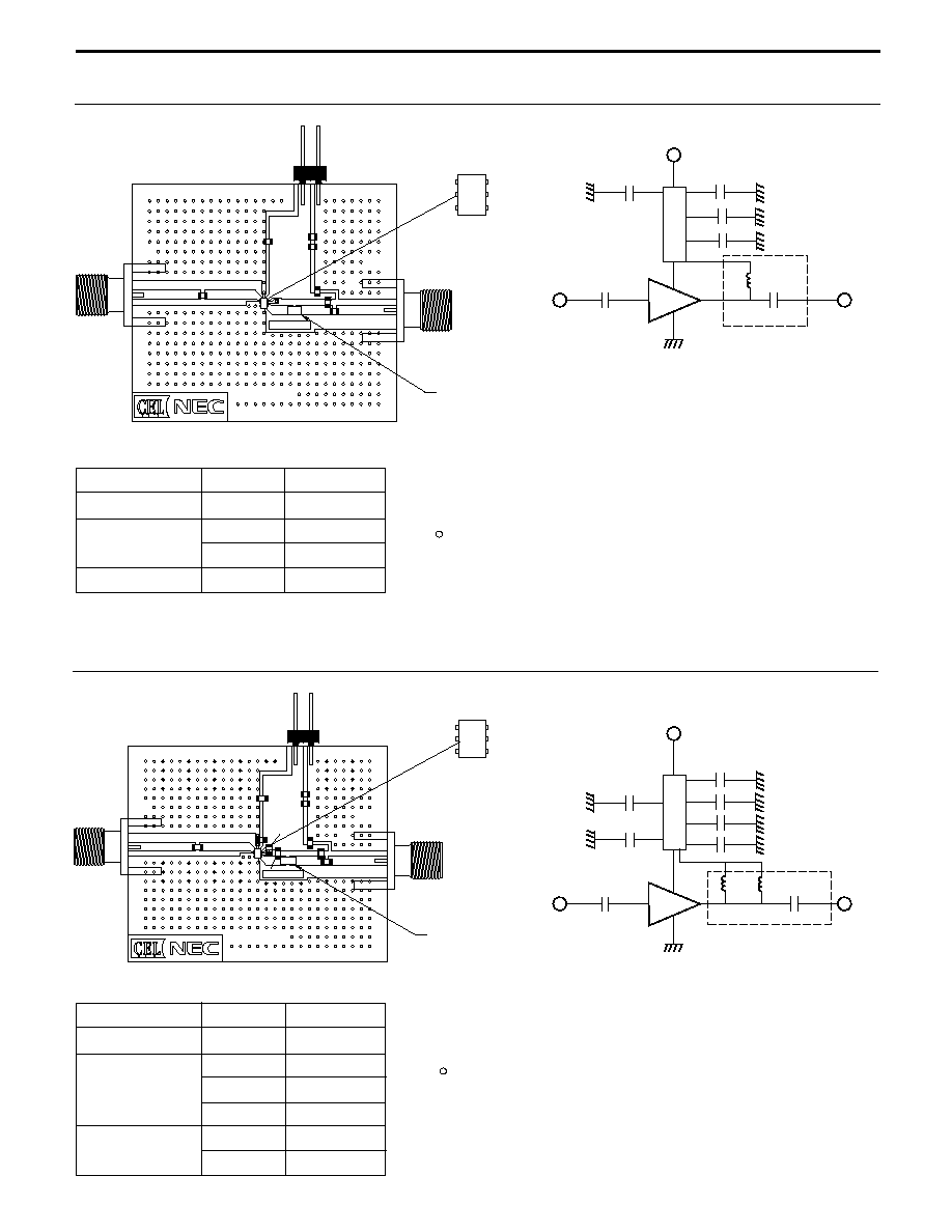
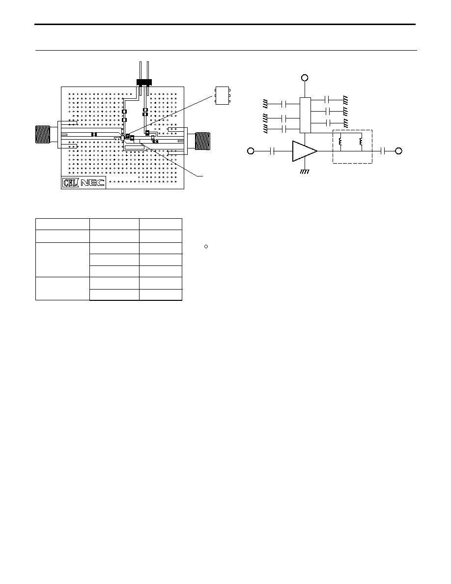
EVALUATION BOARD, 0.9 GHz
1. 1.5 x 1.5 x 0.028", Getek laminate, double sided copper
2. Ground pattern on rear board
3. Solder plated patterns
4. Through holes
EVALUATION BOARD, 1.9 GHz
FORM
SYMBOL
VALUE
Chip Capacitor
C
7,
C
8
10 pF
C
6
.4 pF
C
1,
C
5
51 pF
C
2,
C
3,
C
4
1000 pF
Chip Inductor
L
2
22 nH
L
1
2.7 nH
COMPONENT LIST
1. 1.5 x 1.5 x 0.028", Getek laminate, double sided copper
2. Ground pattern on rear board
3. Solder plated patterns
4. Through holes
C6
C5
J1
C1
C3
L1
U1
C4
J2
GND
P1
Vcc
P2
C2
C3C
C3C
DEVICE ORIENTATION
PIN 1
ADD TAB
H=.028
GETEK
UPC8179TK
IFin
Er=4.2
RFout
Vcc
C6
C5
J1
C1
C3
L1
U1
C4
J2
GND
P1
Vcc
P2
C2
C3C
C3C
DEVICE ORIENTATION
PIN 1
ADD TAB
L2
C7 C8
H=.028
GETEK
UPC8179TK
IFin
Er=4.2
RFout
Vcc
UPC8179TK
FORM
SYMBOL
VALUE
Chip Capacitor
C
6
1 pF
C
1,
C
5
51 pF
C
2
, C
3,
C
4
1800 pF
Chip Inductor
L
1
10 nH
COMPONENT LIST
OUT
50
50
C6
4
1
6
2,3,5
C1
C2
C3
C4
C5
L1
IN
V
CC
OUT
50
50
C
6
1
4
6
2,3,5
C
1
C
2
C
3
C
4
C
7
L
2
L
1
IN
C
5
C
8
V
CC