The information in this document is subject to change without notice. Before using this document, please
confirm that this is the latest version.
Not all products and/or types are available in every country. Please check with an NEC Electronics
sales representative for availability and additional information.
MOS INTEGRATED CIRCUIT
µ
PD120Nxx Series
THREE-TERMINAL LOW-DROPOUT POSITIVE-VOLTAGE REGULATOR
(OUTPUT CURRENT: 0.3 A)
DATA SHEET
Document No. S17145EJ2V0DS00 (2nd edition)
Date Published February 2005 NS CP(K)
Printed in Japan
2005
DESCRIPTION
The
µ
PD120Nxx series provides low-voltage output regulators with the output current capacitance of 0.3 A. The
output voltage varies according to the product (1.5 V, 1.8 V, 2.5 V, or 3.3 V). The circuit current is low due to the
CMOS structure, so the power consumption in the ICs can be reduced. Moreover, since ICs are mounted in the small
package of the
µ
PD120Nxx series, this contributes to the miniaturization of the application set.
FEATURES
∑
Output current: 0.3 A
∑
On-chip overcurrent protection circuit
∑
On-chip thermal protection circuit
∑
Small circuit operation current: 60
µ
A TYP.
APPLICATIONS
Digital TV, Audio, HDD, DVD, etc.
PIN CONFIGURATION (Marking Side)
SC-62
GND
GND
OUTPUT
INPUT
3
2
1
SC-74A
GND
N.C.
GND
OUTPUT
INPUT
1
2
3
5
4

Data Sheet
S17145EJ2V0DS
2
µ
PD120Nxx Series
BLOCK DIAGRAM
+
INPUT
OUTPUT
GND
-
Overcurrent
Protection Circuit
Thermal
Protection Circuit
Error
Amp.
Reference
Voltage
Circuit
Data Sheet
S17145EJ2V0DS
3
µ
PD120Nxx Series
ORDERING INFORMATION
Part Number
Package
Output Voltage
Marking
µ
PD120N15TA SC-74A
1.5
V
K71
µ
PD120N15T1B SC-62
1.5
V
7D
µ
PD120N18TA SC-74A
1.8
V
K72
µ
PD120N18T1B SC-62
1.8
V
7E
µ
PD120N25TA SC-74A
2.5
V
K73
µ
PD120N25T1B SC-62
2.5
V
7F
µ
PD120N33TA SC-74A
.3.3
V
K74
µ
PD120N33T1B SC-62
3.3
V
7G
Remark -E1 or -E2 is suffixed to the end of the part number of taping products, and -A or -AZ to that of Pb-free
products. See the table below for details.
Part Number
Note1
Package Package
Type
µ
PD120NxxTA
SC-74A
∑
Unit
µ
PD120NxxTA-A
Note2
SC-74A
∑
Unit
µ
PD120NxxTA-E1
SC-74A
∑
8 mm wide embossed taping
∑
Pin 1 on take-up side
∑
3000 pcs/reel (MAX.)
µ
PD120NxxTA-E1-A
Note2
SC-74A
∑
8 mm wide embossed taping
∑
Pin 1 on take-up side
∑
3000 pcs/reel (MAX.)
µ
PD120NxxTA-E2
SC-74A
∑
8 mm wide embossed taping
∑
Pin 1 on draw-out side
∑
3000 pcs/reel (MAX.)
µ
PD120NxxTA-E2-A
Note2
SC-74A
∑
8 mm wide embossed taping
∑
Pin 1 on draw-out side
∑
3000 pcs/reel (MAX.)
µ
PD120NxxT1B
SC-62
∑
Unit
µ
PD120NxxT1B-AZ
Note3
SC-62
∑
Unit
µ
PD120NxxT1B-E1
SC-62
∑
12 mm wide embossed taping
∑
Pin 1 on take-up side
∑
1000 pcs/reel (MAX.)
µ
PD120NxxT1B-E1-AZ
Note3
SC-62
∑
12 mm wide embossed taping
∑
Pin 1 on take-up side
∑
1000 pcs/reel (MAX.)
µ
PD120NxxT1B-E2
SC-62
∑
12 mm wide embossed taping
∑
Pin 1 on draw-out side
∑
1000 pcs/reel (MAX.)
µ
PD120NxxT1B-E2-AZ
Note3
SC-62
∑
12 mm wide embossed taping
∑
Pin 1 on draw-out side
∑
1000 pcs/reel (MAX.)
Notes 1. xx stands for symbols that indicate the output voltage.
2. Pb-free (This product does not contain Pb in external electrode and other parts.)
3. Pb-free (This product does not contain Pb in external electrode.)
Data Sheet
S17145EJ2V0DS
4
µ
PD120Nxx Series
ABSOLUTE MAXIMUM RATINGS (T
A
= 25∞C, unless otherwise specified.)
Rating
Parameter Symbol
µ
PD120NxxTA
µ
PD120NxxT1B
Unit
Input Voltage
V
IN
-
0.3 to +6
V
Power Dissipation
Note1
P
T
180/510
Note2
400/2000
Note3
mW
Operating Ambient Temperature
T
A
≠40 to +85
∞C
Operating Junction Temperature
T
J
≠40 to +150
∞C
Storage Temperature
T
stg
≠55 to +150
∞C
Thermal Resistance (junction to ambient)
R
th(J-A)
695/245
Note2
315/62.5
Note3
∞C/W
Note 1. Internally limited. When the operating junction temperature rises over 150
∞
C, the internal circuit shuts down
the output voltage.
2. Mounted on ceramic substrate of 75 mm
2
x 0.7 mm
3. Mounted on ceramic substrate of 16 cm
2
x 0.7 mm
Caution Product quality may suffer if the absolute maximum rating is exceeded even momentarily for any
parameter. That is, the absolute maximum ratings are rated values at which the product is on the
verge of suffering physical damage, and therefore the product must be used under conditions that
ensure that the absolute maximum ratings are not exceeded.
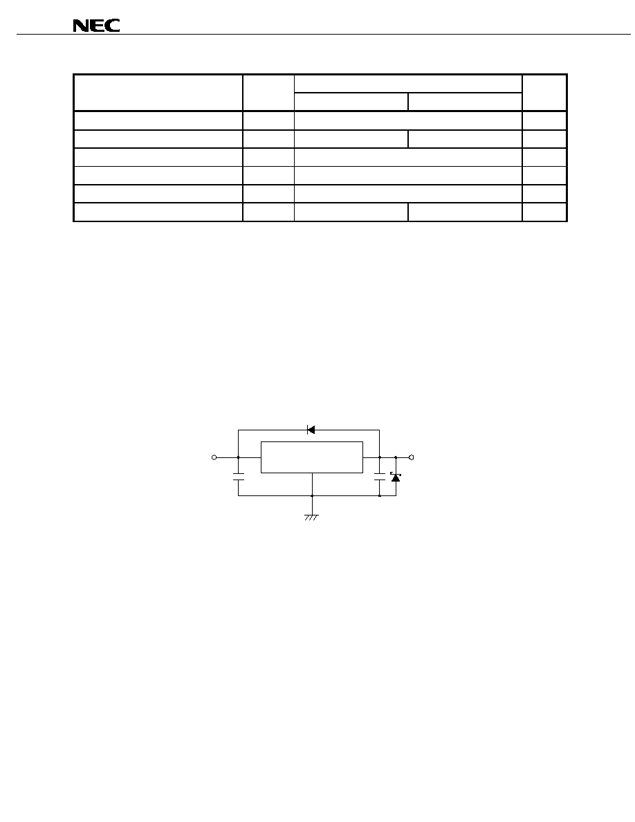
STANDARD CONNECTION
D
2
D
1
C
IN
C
OUT
INPUT
OUTPUT
PD120Nxx
µ
C
IN
: 0.1
µ
F or higher. Set this value according to the length of the line between the regulator and INPUT pin. Be sure
to connect C
IN
to prevent parasitic oscillation. If using a laminated ceramic capacitor, it is necessary to ensure
that C
IN
is 0.1
µ
F or higher for the voltage and temperature range to be used.
C
OUT
: 10
µ
F or higher. Be sure to connect C
OUT
to prevent oscillation and improve excessive load regulation. Place
C
IN
and C
OUT
as close as possible to the IC pins (within 2 cm). Be sure to use the capacitor of 10
µ
F or higher
of capacity values and 1 to 8
of equivalent series resistance under an operating condition.
D
1
: If the OUTPUT pin has a higher voltage than the INPUT pin, connect a diode.
D
2
: If the OUTPUT pin has a lower voltage than the GND pin, connect a schottky barrier diode.
Caution Make sure that no voltage is applied to the OUTPUT pin from external.
Data Sheet
S17145EJ2V0DS
5
µ
PD120Nxx Series
RECOMMENDED OPERATING CONDITIONS
Parameter Symbol
Type
Number
MIN.
TYP.
MAX.
Unit
µ
PD120N15 3.0
5.5
V
µ
PD120N18 3.2
5.5
V
µ
PD120N25
4.5 5.5 V
Input Voltage
V
IN
µ
PD120N33 4.5
5.5
V
Output Current
I
O
All
0 0.3
A
Operating Ambient Temperature T
A
All
-
40
+
85
∞
C
Operating Junction Temperature T
J
All
-
40
+
125
∞
C
Caution Use of conditions other than the above-listed recommended operating conditions is not a problem
as long as the absolute maximum ratings are not exceeded. However, since the use of such
conditions diminishes the margin of safety, careful evaluation is required before such conditions are
used. Moreover, using the MAX. value for all the recommended operating conditions is not
guaranteed to be safe.
ELECTRICAL CHARACTERISTICS
µ
PD120N15
(T
J
= 25
∞
C, V
IN
= 5.0 V, I
O
= 0.15 A, C
IN
= 0.1
µ
F, C
OUT
= 10
µ
F, unless otherwise specified.)
Parameter Symbol
Conditions
MIN.
TYP.
MAX.
Unit
V
O1
1.47
1.5
1.53 V
Output Voltage
V
O2
3.0
V
V
IN
5.5 V, 0 A
I
O
0.3 A
1.455
-
1.545 V
Line Regulation
REG
IN
3.0
V
V
IN
5.5 V
-
1 30
mV
Load Regulation
REG
L
0
A
I
O
0.3 A
-
2 30
mV
Quiescent Current
I
BIAS
I
O
= 0 A
-
60 120
µ
A
Quiescent Current Change
I
BIAS
3.0
V
V
IN
5.5 V
-
-
25
µ
A
Output Noise Voltage
V
n
10
kHz
f
100 kHz
-
100
-
µ
V
r.m.s.
Ripple Rejection
R∑R
f = 1 kHz, 3.0 V
V
IN
5.5 V
-
63
-
dB
I
O
= 0.15 A
-
0.6 0.9 V
Dropout Voltage
V
DIF
I
O
= 0.3 A
-
1.0
-
V
Short Circuit Current
I
Oshort
V
IN
= 5 V
-
0.2
-
A
Peak Output Current
I
Opeak
V
IN
= 5 V
0.3
-
-
A
Temperature Coefficient of
Output Voltage
V
O
/
T I
O
= 0 A, 0
∞
C
T
J
125
∞
C
-
0.01
-
mV/
∞
C
µ
PD120N18
(T
J
= 25
∞
C, V
IN
= 5.0 V, I
O
= 0.15 A, C
IN
= 0.1
µ
F, C
OUT
= 10
µ
F, unless otherwise specified.)
Parameter Symbol
Conditions
MIN.
TYP.
MAX.
Unit
V
O1
1.764
1.8
1.836
V
Output Voltage
V
O2
3.2
V
V
IN
5.5 V, 0 A
I
O
0.3 A
1.746
-
1.854 V
Line Regulation
REG
IN
3.2
V
V
IN
5.5 V
-
1 30
mV
Load Regulation
REG
L
0
A
I
O
0.3 A
-
2 30
mV
Quiescent Current
I
BIAS
I
O
= 0 A
-
60 120
µ
A
Quiescent Current Change
I
BIAS
3.2
V
V
IN
5.5 V
-
-
25
µ
A
Output Noise Voltage
V
n
10
kHz
f
100 kHz
-
120
-
µ
V
r.m.s.
Ripple Rejection
R∑R
f = 1 kHz, 3.2 V
V
IN
5.5 V
-
63
-
dB
Dropout Voltage
V
DIF
I
O
= 0.15 A
-
0.4 0.65 V
Short Circuit Current
I
Oshort
V
IN
= 5 V
-
0.2
-
A
Peak Output Current
I
Opeak
V
IN
= 5 V
0.3
-
-
A
Temperature Coefficient of
Output Voltage
V
O
/
T I
O
= 0 A, 0
∞
C
T
J
125
∞
C
-
0.01
-
mV/
∞
C