©
1995
DATA SHEET
MOS INTEGRATED CIRCUIT
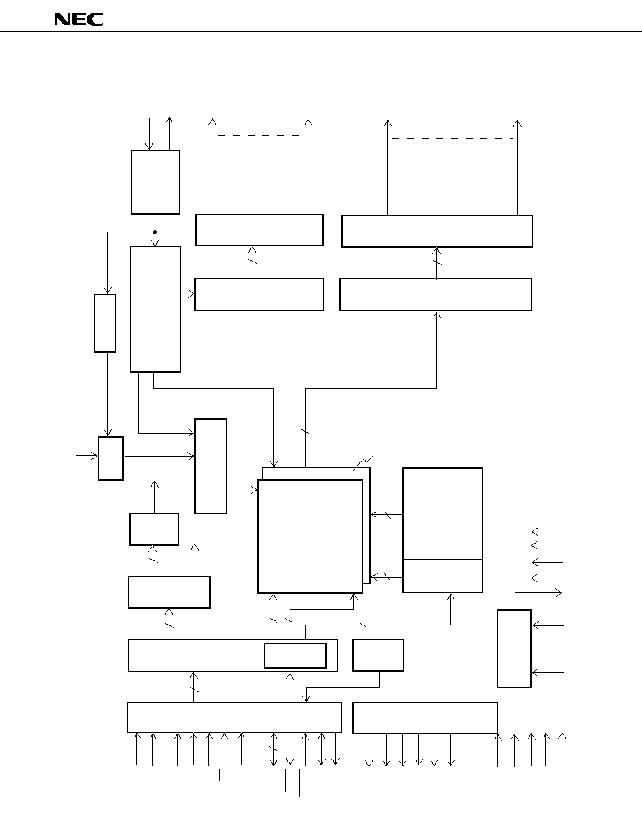
DESCRIPTION
The
µ
PD16435 and 16435A are controllers/drivers for a 119
◊
73-dot LCD, and perform LCD full-dot and character
composite display by means of control by a microprocessor that has a 4 or 8-bit data bus. A charge pump type
DC/DC converter is also incorporated, enabling 3 or 5 V single power supply drive.
The
µ
PD16435 uses an external reference clock. The
µ
PD16435A has the on-chip oscillation circuit (external
crystal resonator).
FEATURES
∑
Can interface to 4 or 8-bit CPU.
∑
Incorporates 119 segment outputs and 73 common outputs.
(Display duty selectable from 1/35, 1/37, 1/71, 1/73)
∑
5
◊
7 character font 208 character data configuration character generation ROM and 16 character data configuration
character generation RAM, allowing composite full-dot and character display
∑
Incorporates extended display functions such as magnification, lateral scrolling, blink, reverse, etc.
∑
Operating voltage: 2.7 V to 5.5 V
∑
On-chip DC/DC converter: Selectable between
◊
4 set-up circuit and
◊
2 step-up circuit
∑
On-chip temperature correction circuit
∑
Master/slave operation capability
∑
On-chip power-on reset circuit
∑
On-chip oscillation circuit (
µ
PD16435A)
∑
232-pin TCP (Tape Carried Package)
ORDERING INFORMATION
Part Number
Package
µ
PD16435N-001-
◊◊◊
TCP (TAB), Standard ROM code
µ
PD16435N-001-001
Standard quad TCP (Conforms to EIAJ), Standard ROM code
µ
PD16435N-001-002
Standard dual TCP (Output OLB: 0.25 mm pitch), Standard ROM code
µ
PD16435AN-001-
◊◊◊
TCP (TAB), Standard ROM code
µ
PD16435AN-001-001
Standard quad TCP (Conforms to EIAJ), Standard ROM code
µ
PD16435AN-001-052
Standard dual TCP (Output OLB: 0.25 mm pitch), Standard ROM code
Explanation of Part Number
µ
PD16435 (A) N-xxx-xxx
TCP code
ROM code
The TCP model is a custom model. For details, consult NEC sales representative.
Document No. S10298EJ3V0DS00 (3rd edition)
Date Published April 1997 N
Printed in Japan
DOT MATRIX LCD CONTROLLER/DRIVER
µ
PD16435, 16435A
µ
PD16435, 16435A
4
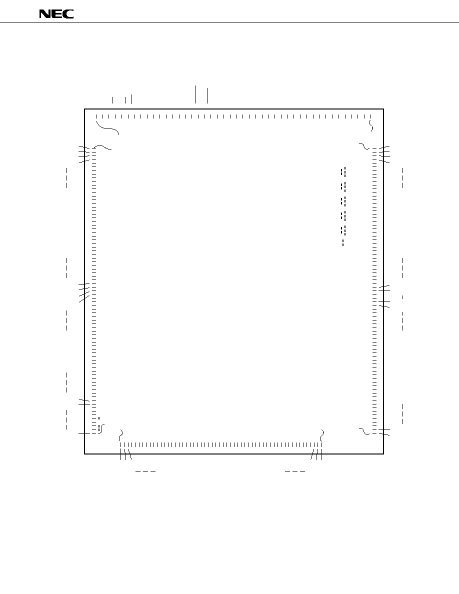
PIN DESCRIPTIONS
Description
Chip select signal
Register selection signal (specifies address register when "0",
control register when "1").
Read enable signal. Reads write address when scrolling.
Active edge is falling edge.
Write enable signal.
Active edge is falling edge.
Word length selection signal (4-bit input when "1", 8-bit input
when "0").
Transmit/receive data (3-state bidirectional)
Upper
D4 to D7
Lower
D0 to D3 (These pins should be set as unused in case
of 4-bit data).
In test mode, these pins are output pins.
In a 4-bit transfer, storage is performed in the upper (MSB) in
order from the data transferred first.
"0" indicates busy state.
"0"
Initialization of all internal registers and commands is
performed. Output is fixed at V
1
.
Signal is output to CPU on completion of one-character scroll.
Synchronization signal input/output pins for master/slave
operation.
µ
PD16435: Input the 4.19 MHz reference clock to the OSC
1
pin
externally. Leave the OSC
2
pin open. (Always outputs high
level.)
µ
PD16435A: This is the pin to which the 4.19 MHz crystal
resonator is connected. Input the external clock to OSC
1
first.
2 Hz external clock input pin. Scaled by 2 internally to generate 1
Hz, used as blink synchronization signal.
Common output signals
Segment output signals
"1"
Test mode
"0" or open
Normal operating mode
Output Type
≠≠≠
≠≠≠
≠≠≠
≠≠≠
≠≠≠
CMOS 3-state
Nch open-drain
≠≠≠
CMOS
Nch open-drain
≠≠≠
≠≠≠
Analog switch
Analog switch
≠≠≠
Input/Output
Input
Input
Input (Schmitt)
Input (Schmitt)
Input
Input/output
Output
Input
Output
Input/output
≠≠≠
Input (Schmitt)
Output
Output
Output
Pin Name
Pin No.
CS
255
RS
254
RD
253
WR
252
WS
251
250
D
0
to D
7
to
243
BUSY
240
RESET
242
SCR
241
SYNC
239
OSC
1
235
OSC
2
234
OSC
3
233
COM1 to
212 to 176
COM73
3 to 38
SEG1 to
41 to 70
SEG119
81 to 134
137 to 171
TEST1
238
TEST2
237
µ
PD16435, 16435A
5
Pin Name
Pin No.
V1
221
220
V2 to V5
to
217
V
IN
(≠)
224
V
IN
(+)
223
V
CC
, GND1
232, 256
V
DD
, GND2
257, 222
3/5
236
C1
±
, C2
±
,
230 to
C3
±
225
Description
LCD drive power supply pin
Internal OP-amp output
LCD drive power supply pins
Can be adjusted by addition of external resistor.
Liquid crystal drive power supply OP-amp input pins
Logic power supply, GND
Liquid crystal drive (step-up) power supply, GND
Drive voltage selection pin
"1"
V
DD
= 3 V (
◊
4 step-up circuit selected)
"0"
V
DD
= 5 V (
◊
2 step-up circuit selected)
A 1
µ
F tantalum or ceramic capacitor should be connected
externally.
Input/Output
Output
Input
Input
≠≠≠
≠≠≠
Input
≠≠≠
Output Type
≠≠≠
≠≠≠
≠≠≠
≠≠≠
≠≠≠
≠≠≠
≠≠≠
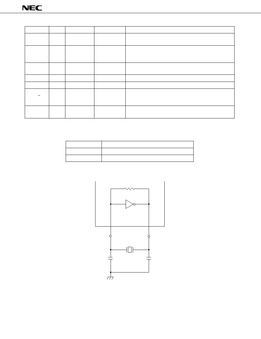
REFERENCE CLOCK
Product Name
Reference Clock
µ
PD16435
External input
µ
PD16435A
On-chip oscillation circuit (External crystal resonator)
OSC CIRCUIT (
µ
PD16435A)
OSC
2
OSC
1
4.19 MHz