 | –≠–ª–µ–∫—Ç—Ä–æ–Ω–Ω—ã–π –∫–æ–º–ø–æ–Ω–µ–Ω—Ç: UPD16448A | –°–∫–∞—á–∞—Ç—å:  PDF PDF  ZIP ZIP |
Document Outline
- COVER
- FEATURES
- ORDERING INFORMATION
- BLOCK DIAGRAM
- SAMPLE AND HOLD CIRCUIT AND OUTPUT CIRCUIT
- PIN CONFIGRATION (uPD16448A N-xxx)
- 1. PIN DESCRIPTION
- 2. FUNCTION DESCRIPTION
- 2.1 Multiplexer Circuit
- 2.1.1 Vertical stripe array mode (MP/TH = L, MP/1.5 = L)
- 2.1.2 Single-side delta array mode (MP/TH = L, MP/1.5 = H)
- 2.1.3 Double-side delta array mode (MP/TH = H, MP/1.5 = H)
- 2.1.4 Mosaic array mode (MP/TH = H, MP/1.5 = L)
- 2.1.5 Relation between Shift Clock CLIn and Internal Sampling Pulse SHPn
- 2.2 Sample and Hold Circuit
- 2.3 Write Operation Timing
- 3.ELECTRICAL CHARACTERISTICS
- 4. RECOMMENDED CONDITIONS FOR INSTALLATION

Document No. S11712EJ3V0DS00 (3rd edition)
Date Published August 1998 NS CP(K)
Printed in Japan
SOURCE DRIVER FOR 240-OUTPUT TFT-LCD
(NAVIGATION, AUTOMOBILE LCD-TV)
DATA SHEET
MOS INTEGRATED CIRCUIT
µ
µ
µ
µ
PD16448A
©
1998
The mark
5
5
5
5
shows major revised points.
µ
PD16448A is a source driver for TFT liquid crystal panels. This IC consists of a multiplexer circuit supporting a
variety of pixel arrays, a shift register that generates sampling timing, and two sample and hold circuits that sample
analog voltages. Because the two sample and hold circuits alternately execute sampling and holding, a high
definition can be obtained.
In addition, simultaneous sampling and successive sampling are automatically selected according to the pixel
array of the LCD panel. It is ideal for a wide range of applications, including navigation systems and automobile LCD-
TVs.
FEATURES
∑
Can be driven on 5 V (Dynamic range: 4.3 V, V
DD2
= 5.0 V)
∑
240-output
∑
f
max.
= 18 MHz (V
DD1
= 3.0 V)
∑
Simultaneous/successive sampling selectable according to pixel array
Simultaneous sampling: vertical stripe
Successive sampling:
delta array, mosaic array
∑
Two sample and hold circuits
∑
Low output deviation between pins (
±
20 mV MAX.)
∑
Stripe, delta, and mosaic pixel arrays supported by internal multiplexer circuit
∑
Left and right shift selected by R/L pin
∑
Single-side mounting possible
ORDERING INFORMATION
Part Number
Package
µ
PD16448AN-
◊◊◊
TCP (TAB package)
Remark The dimensions of TCP are custom-made. Please consult NEC for details.
The information in this document is subject to change without notice.

2
µ
µ
µ
µ
PD16448A
BLOCK DIAGRAM
CLI
1 to 3
R/L
240-bit shift register
STHR
STHL
Multi-
plexer
INH
RESET
C
2
C
1
C
3
MP/TH
MP/1.5
240-bit level shifter
H
1
H
240
.....................................................................................................
240-bit sample and hold buffer
+3.3 V
V
DD1
V
SS1
V
SS2
V
SS3
GND
+5.0 V
V
DD2
3
SAMPLE AND HOLD CIRCUIT AND OUTPUT CIRCUIT
Swa1
C
H1
+
≠
Swb1
Swa2
C
H2
+
≠
Swb2
H
n
VIDEO
LINE
3
µ
µ
µ
µ
PD16448A
PIN CONFIGRATION (
µ
µ
µ
µ
PD16448A N-xxx)
Remark
This figure does not spesify the TCP package.
C
1
C
2
C
3
V
DD2
V
DD1
STHL
MP/TH
MP/1.5
R/L
RESET
INH
CLI
1
CLI
2
CLI
3
TEST
STHR
V
SS1
V
SS3
V
SS2
H
240
H
239
H
238
H
237
∑
∑
∑
∑
∑
∑
∑
∑
∑
∑
H
5
H
4
H
3
H
2
H
1
Copper Foll
suface
5
4
µ
µ
µ
µ
PD16448A
1. PIN DESCRIPTION
Symbol
Name
Function
C
1
to C
3
Video signal input
Input R, G, and B video signals.
H
1
to H
240
Video signal output
Video signal output pins. Output sampled and held video signals during
horizontal period.
STHR
STHL
Cascade I/O
Start pulse I/O pins of sample hold timing. STHR serves as an input pin
and STHL, as an output pin, in the case of right shift. In the case of left
shift, STHL serves as an input pin, and STHR, as an output pin.
CLI
1
CLI
2
CLI
3
Shift clock input
A start pulse is read at the rising edge of CLI
1
. Sampling pulse SHP
n
is
generated at the rising edge of CLI
1
through CLI
3
during successive
sampling, and at the rising edge of CLI
1
during simultaneous sampling
(for details, refer to the Timing charts in 2.FUNCTION DESCRIPTION).
INH
Inhibit input
Selects a multiplexer and one of the two sample and hold circuits at the
falling edge.
RESET
Reset input
Resets the select counter of the multiplexer and the selector circuit of
the two sample and hold circuits when it goes high. After reset, the
multiplexer is turned OFF, so sure to input one pulse of the INH signal
before inputting the video signal. If the video signal is input without the
INH signal, sampling is not executed.
Four types of color filter arrays can be supported by combination of
MP/TH and MP/1.5.
Mode
MP/TH
MP/1.5
MP/TH
Multiplexer circuit select input (1)
Vertical stripe array
L
L
Single-side delta array
L
H
Mosaic array
H
L
Double-side delta array
H
H
MP/1.5
Multiplexer circuit select input (2)
R/L
Shift direction select input
R/L = H; right shift: STHR
H
1
H
240
STHL
R/L = L; left shift: STHL
H
240
H
1
STHR
V
DD1
Logic power supply
3.0 V to 5.5 V
V
DD2
Driver power supply
5.0 V
±
0.5 V
V
SS1
Logic ground
Connect this pin to ground of system.
V
SS2
Driver ground
Connect this pin to ground of system.
V
SS3
Driver ground
Connect this pin to ground of system.
TEST
Test pin
Fix this pin to L.
5
µ
µ
µ
µ
PD16448A
2. FUNCTION DESCRIPTION
2.1 Multiplexer Circuit
This circuit selects RGB video signals input to the C
1
, C
2
, and C
3
pins according to the pixel array of the liquid
crystal panel, and outputs the signals to the H
1
through H
240
pins.
Vertical stripe array, single-/double-side delta array, or mosaic array can be selected by using the MP/TH and
MP/1.5 pins.
2.1.1 Vertical stripe array mode (MP/TH = L, MP/1.5 = L)
In this mode, the relation between video signals C
1
, C
2
, and C
3
, and output pins is as shown below. This
mode is used to drive a panel of vertical stripe array. In this mode, the multiplexer circuit is in the through
status.
Relation between video signals C
1
, C
2
, and C
3
, and output pins (during right shift)
Line No.
(number of
INHs)
RESET
INH
H
1
(H
240
)
H
2
(H
239
)
H
3
(H
238
)
H
4
(H
237
)
H
239
(H
2
)
H
240
(H
1
)
0
H
L
Sampling
C
1
(C
3
)
Sampling
C
2
(C
2
)
Sampling
C
3
(C
1
)
Sampling
C
1
(C
3
)
Sampling
C
2
(C
2
)
Sampling
C
3
(C
1
)
1
L
Output
C
1
(C
3
)
Output
C
2
(C
2
)
Output
C
3
(C
1
)
Output
C
1
(C
3
)
Output
C
2
(C
2
)
Output
C
3
(C
1
)
2
L
Output
C
1
(C
3
)
Output
C
2
(C
2
)
Output
C
3
(C
1
)
Output
C
1
(C
3
)
Output
C
2
(C
2
)
Output
C
3
(C
1
)
3
L
Output
C
1
(C
3
)
Output
C
2
(C
2
)
Output
C
3
(C
1
)
Output
C
1
(C
3
)
Output
C
2
(C
2
)
Output
C
3
(C
1
)
:
:
:
:
:
:
:
:
:
:
:
:
:
:
:
:
:
:
( ) indicates the case of left shift.
Pixel arrangement of vertical stripe array and multiplexer operation
R
C
1
B
C
2
G
C
3
PD16448A
Right shift (R/L = "H"), MP/TH = "L", MP/1.5 = "L"
µ
H
1
R
R
R
R
R
B
B
B
B
B
G
G
G
G
G
R
R
R
R
R
B
B
B
B
B
G
G
G
G
G
R
R
R
R
R
H
2
H
3
H
4
H
5
H
6
H
7
6
µ
µ
µ
µ
PD16448A
Timing chart of vertical stripe array
RESET
INH
H
1
(H
240
)
sampling
input data
Output
Un-
defined
C
1
(C
3
)
C
1
(C
3
)
C
1
(C
3
)
C
1
(C
3
)
C
1
(C
3
)
Undefined
C
1
(C
3
)
C
1
(C
3
)
C
1
(C
3
)
C
1
(C
3
)
C
1
(C
3
)
H
2
(H
239
)
sampling
input data
Output
Un-
defined
C
2
(C
2
)
C
2
(C
2
)
C
2
(C
2
)
C
2
(C
2
)
C
2
(C
2
)
Undefined
C
2
(C
2
)
C
2
(C
2
)
C
2
(C
2
)
C
2
(C
2
)
C
2
(C
2
)
H
3
(H
238
)
sampling
input data
Output
Un-
defined
C
3
(C
1
)
C
3
(C
1
)
C
3
(C
1
)
C
3
(C
1
)
C
3
(C
1
)
Undefined
C
3
(C
1
)
C
3
(C
1
)
C
3
(C
1
)
C
3
(C
1
)
C
3
(C
1
)
H
239
(H
2
)
sampling
input data
Output
Un-
defined
C
2
(C
2
)
C
2
(C
2
)
C
2
(C
2
)
C
2
(C
2
)
C
2
(C
2
)
Undefined
C
2
(C
2
)
C
2
(C
2
)
C
2
(C
2
)
C
2
(C
2
)
C
2
(C
2
)
H
240
(H
1
)
sampling
input data
Output
Un-
defined
C
3
(C
1
)
C
3
(C
1
)
C
3
(C
1
)
C
3
(C
1
)
C
3
(C
1
)
Undefined
C
3
(C
1
)
C
3
(C
1
)
C
3
(C
1
)
C
3
(C
1
)
C
3
(C
1
)
7
µ
µ
µ
µ
PD16448A
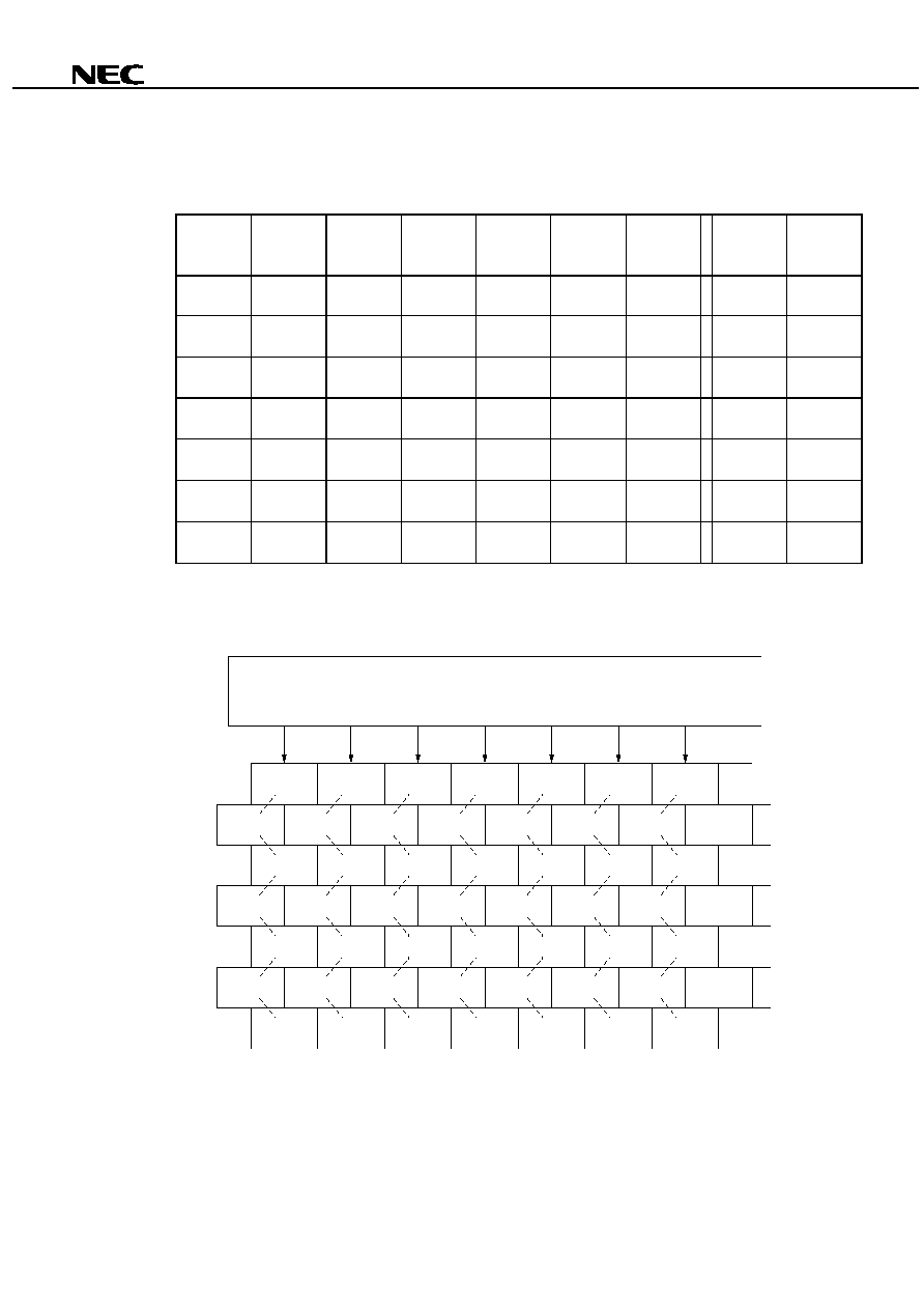
2.1.2 Single-side delta array mode (MP/TH = L, MP/1.5 = H)
Relation between video signals C
1
, C
2
, and C
3
, and output pins
Line No.
(number of
INHs)
RESET
INH
H
1
(H
240
)
H
2
(H
239
)
H
3
(H
238
)
H
4
(H
237
)
H
239
(H
2
)
H
240
(H
1
)
0
H
L
Undefined
Undefined
Undefined
Undefined
Undefined
Undefined
1
L
Sampling
C
1
(C
3
)
Sampling
C
2
(C
2
)
Sampling
C
3
(C
1
)
Sampling
C
1
(C
3
)
Sampling
C
2
(C
2
)
Sampling
C
3
(C
1
)
2
L
Output
C
1
(C
3
)
Output
C
2
(C
2
)
Output
C
3
(C
1
)
Output
C
1
(C
3
)
Output
C
2
(C
2
)
Output
C
3
(C
1
)
3
L
Output
C
2
(C
1
)
Output
C
3
(C
3
)
Output
C
1
(C
2
)
Output
C
2
(C
1
)
Output
C
3
(C
3
)
Output
C
1
(C
2
)
4
L
Output
C
1
(C
3
)
Output
C
2
(C
2
)
Output
C
3
(C
1
)
Output
C
1
(C
3
)
Output
C
2
(C
2
)
Output
C
3
(C
1
)
5
L
Output
C
2
(C
1
)
Output
C
3
(C
3
)
Output
C
1
(C
2
)
Output
C
2
(C
1
)
Output
C
3
(C
3
)
Output
C
1
(C
2
)
( ) indicates the case of left shift.
Pixel arrangement of single-side delta array and multiplexer operation
R
C
1
B
C
2
G
C
3
PD16448A
Right shift (R/L = H), MP/TH = "L", MP/1.5 = "H"
µ
H
1
R
B
G
R
B
G
R
H
2
H
3
H
4
H
5
H
6
H
7
B
G
R
B
G
R
B
G
R
B
G
R
B
G
R
B
G
R
B
G
R
B
G
R
B
G
R
B
G
R
B
G
R
B
G
R
B
G
R
B
G
R
B
G
R
8
µ
µ
µ
µ
PD16448A
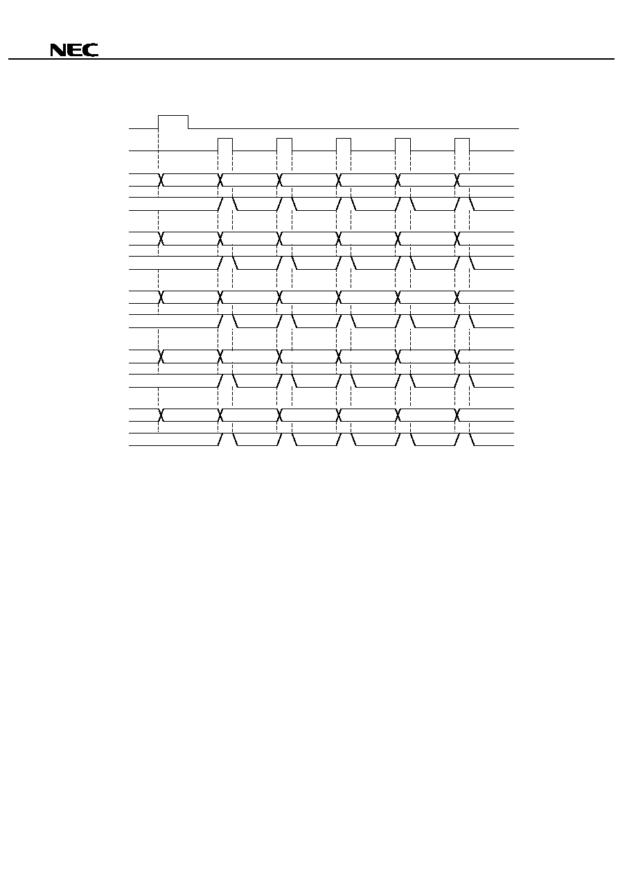
Timing chart of single-side delta array
RESET
INH
H
1
(H
240
)
sampling
input data
Output
Un-
defined
Undefined
C
1
(C
3
)
C
2
(C
1
)
C
1
(C
3
)
C
2
(C
1
)
Undefined
C
1
(C
3
)
C
2
(C
1
)
C
1
(C
3
)
C
2
(C
1
)
H
2
(H
239
)
sampling
input data
Output
Un-
defined
Undefined
C
2
(C
2
)
C
3
(C
3
)
C
2
(C
2
)
C
3
(C
3
)
Undefined
Undefined
C
2
(C
2
)
C
3
(C
3
)
C
2
(C
2
)
C
3
(C
3
)
H
3
(H
238
)
sampling
input data
Output
Un-
defined
Undefined
C
3
(C
1
)
C
1
(C
2
)
C
3
(C
1
)
C
1
(C
2
)
Undefined
Undefined
C
3
(C
1
)
C
1
(C
2
)
C
3
(C
1
)
C
1
(C
2
)
H
239
(H
2
)
sampling
input data
Output
Un-
defined
Undefined
C
2
(C
2
)
C
3
(C
3
)
C
2
(C
2
)
C
3
(C
3
)
Undefined
Undefined
C
2
(C
2
)
C
3
(C
3
)
C
2
(C
2
)
C
3
(C
3
)
H
240
(H
1
)
sampling
input data
Output
Un-
defined
Undefined
C
3
(C
1
)
C
1
(C
2
)
C
3
(C
1
)
C
1
(C
2
)
Undefined
Undefined
C
3
(C
1
)
C
1
(C
2
)
C
3
(C
1
)
C
1
(C
2
)
9
µ
µ
µ
µ
PD16448A
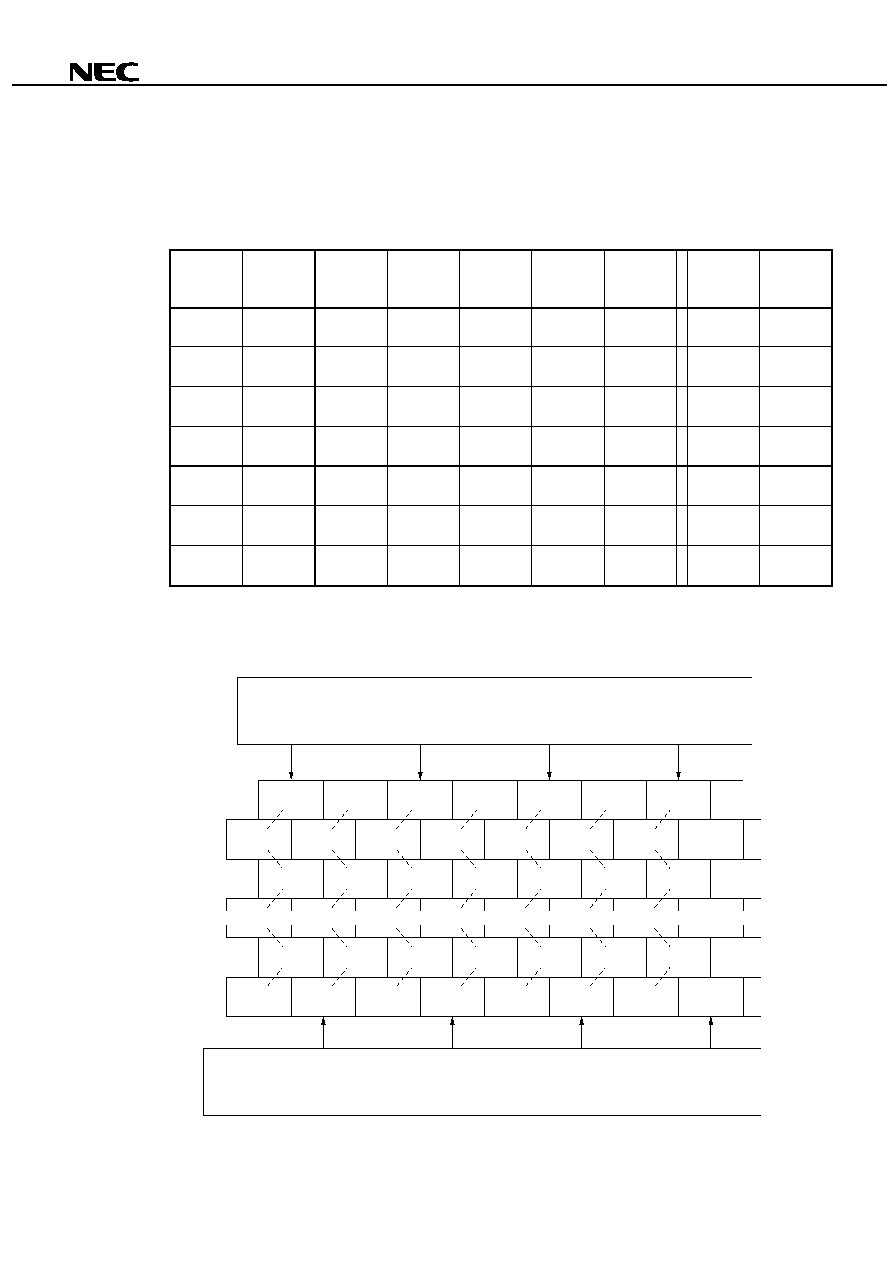
2.1.3 Double-side delta array mode (MP/TH = H, MP/1.5 = H)
Because the pad pitch of the
µ
PD16448A is designed so that the IC is mounted on one side, the output
pitch must be expanded on the TCP if the IC is mounted on both sides.
Relation between video signals C
1
, C
2
, and C
3
, and output pins
Line No.
(number of
INHs)
RESET
INH
H
1
(H
240
)
H
2
(H
239
)
H
3
(H
238
)
H
4
(H
237
)
H
239
(H
2
)
H
240
(H
1
)
0
H
L
Undefined
Undefined
Undefined
Undefined
Undefined
Undefined
1
L
Sampling
C
2
(C
3
)
Sampling
C
3
(C
2
)
Sampling
C
1
(C
1
)
Sampling
C
2
(C
3
)
Sampling
C
3
(C
2
)
Sampling
C
1
(C
1
)
2
L
Output
C
2
(C
3
)
Output
C
3
(C
2
)
Output
C
1
(C
1
)
Output
C
2
(C
3
)
Output
C
3
(C
2
)
Output
C
1
(C
1
)
3
L
Output
C
1
(C
1
)
Output
C
2
(C
3
)
Output
C
3
(C
2
)
Output
C
1
(C
1
)
Output
C
2
(C
3
)
Output
C
3
(C
2
)
4
L
Output
C
2
(C
3
)
Output
C
3
(C
2
)
Output
C
1
(C
1
)
Output
C
2
(C
3
)
Output
C
3
(C
2
)
Output
C
1
(C
1
)
5
L
Output
C
1
(C
1
)
Output
C
2
(C
3
)
Output
C
3
(C
2
)
Output
C
1
(C
1
)
Output
C
2
(C
3
)
Output
C
3
(C
2
)
( ) indicates the case of left shift.
Pixel arrangement of double-side delta array and multiplexer operation
R
C
1
B
C
2
G
C
3
PD16448A
Right shift (R/L = "H"), MP/TH = "H", MP/1.5 = "H"
µ
H
1
R
B
G
R
B
G
R
H
2
H
3
H
3
B
G
R
B
G
R
B
G
R
B
G
R
B
G
R
R
B
G
R
B
G
R
B
G
R
B
G
R
B
G
G
C
1
R
C
2
B
C
3
PD16448A
Left shift (R/L = "L"), MP/TH = "H", MP/1.5 = "H"
µ
H
240
H
239
H
238
H
237

10
µ
µ
µ
µ
PD16448A
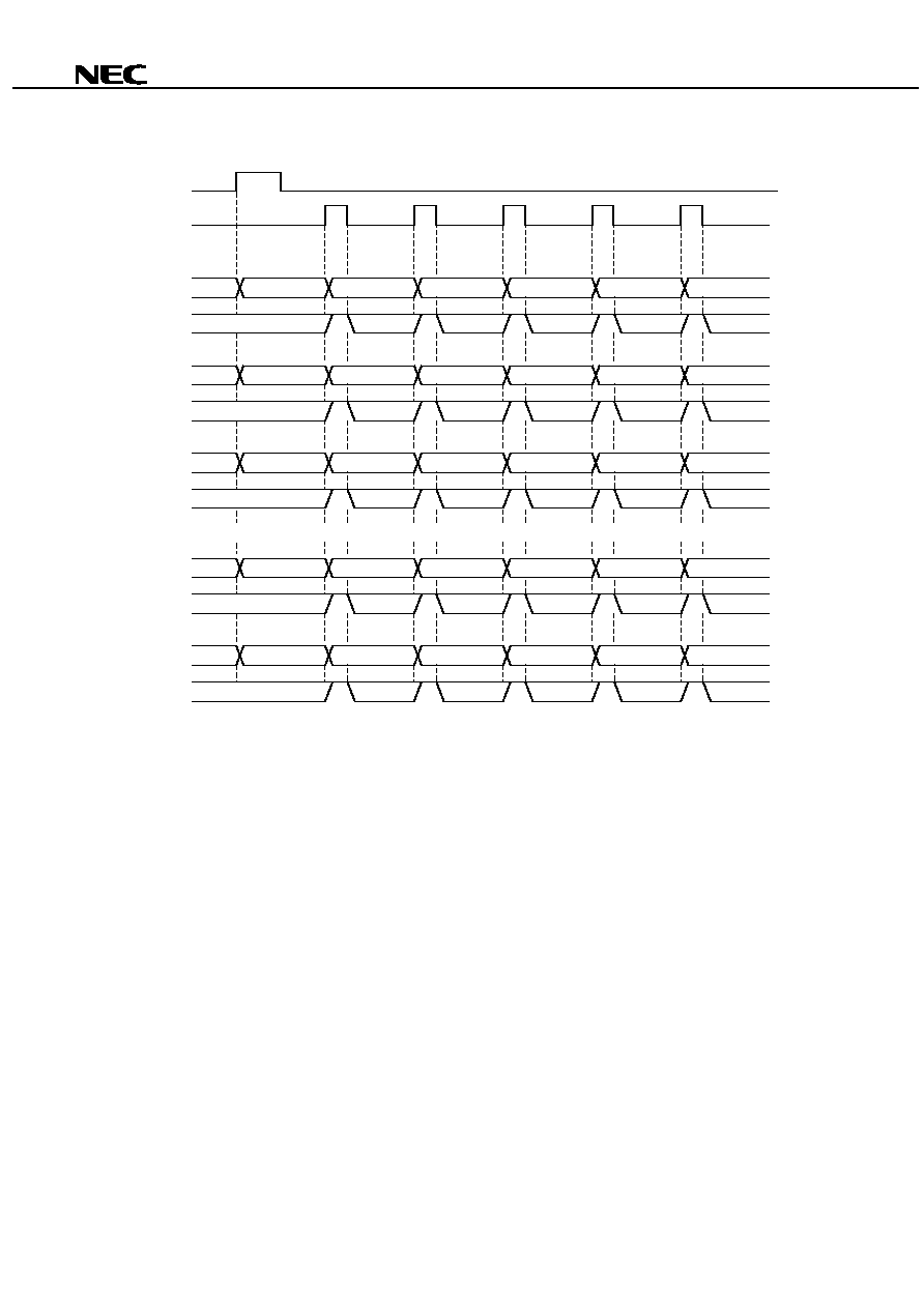
Timing chart of double-side delta array
RESET
INH
H
1
(H
240
)
sampling
input data
Output
Un-
defined
Undefined
C
2
(C
3
)
C
1
(C
1
)
C
2
(C
3
)
C
1
(C
1
)
Undefined
C
2
(C
3
)
C
1
(C
1
)
C
2
(C
3
)
C
1
(C
1
)
H
2
(H
239
)
sampling
input data
Output
Un-
defined
Undefined
C
3
(C
2
)
C
2
(C
3
)
C
3
(C
2
)
C
2
(C
3
)
Undefined
Undefined
C
3
(C
2
)
C
2
(C
3
)
C
3
(C
2
)
C
2
(C
3
)
H
3
(H
238
)
sampling
input data
Output
Un-
defined
Undefined
C
1
(C
1
)
C
3
(C
2
)
C
1
(C
1
)
C
3
(C
2
)
Undefined
Undefined
C
1
(C
1
)
C
3
(C
2
)
C
1
(C
1
)
C
3
(C
2
)
H
239
(H
2
)
sampling
input data
Output
Un-
defined
Undefined
C
3
(C
2
)
C
2
(C
3
)
C
3
(C
2
)
C
2
(C
3
)
Undefined
Undefined
C
3
(C
2
)
C
2
(C
3
)
C
3
(C
2
)
C
2
(C
3
)
H
240
(H
1
)
sampling
input data
Output
Un-
defined
Undefined
C
1
(C
1
)
C
3
(C
2
)
C
1
(C
1
)
C
3
(C
2
)
Undefined
Undefined
C
1
(C
1
)
C
3
(C
2
)
C
1
(C
1
)
C
3
(C
2
)

11
µ
µ
µ
µ
PD16448A
2.1.4 Mosaic array mode (MP/TH = H, MP/1.5 = L)
Relation between video signals C
1
, C
2
, and C
3
, and output pins
Line No.
(number of
INHs)
RESET
INH
H
1
(H
240
)
H
2
(H
239
)
H
3
(H
238
)
H
4
(H
237
)
H
239
(H
2
)
H
240
(H
1
)
0
H
L
Undefined
Undefined
Undefined
Undefined
Undefined
Undefined
1
L
Sampling
C
1
(C
3
)
Sampling
C
2
(C
2
)
Sampling
C
3
(C
1
)
Sampling
C
1
(C
3
)
Sampling
C
2
(C
2
)
Sampling
C
3
(C
1
)
2
L
Output
C
1
(C
3
)
Output
C
2
(C
2
)
Output
C
3
(C
1
)
Output
C
1
(C
3
)
Output
C
2
(C
2
)
Output
C
3
(C
1
)
3
L
Output
C
3
(C
2
)
Output
C
1
(C
1
)
Output
C
2
(C
3
)
Output
C
3
(C
2
)
Output
C
1
(C
1
)
Output
C
2
(C
3
)
4
L
Output
C
2
(C
1
)
Output
C
3
(C
3
)
Output
C
1
(C
2
)
Output
C
2
(C
1
)
Output
C
3
(C
3
)
Output
C
1
(C
2
)
5
L
Output
C
1
(C
3
)
Output
C
2
(C
2
)
Output
C
3
(C
1
)
Output
C
1
(C
3
)
Output
C
2
(C
2
)
Output
C
3
(C
1
)
:
:
:
:
:
:
:
:
:
:
:
:
:
:
:
:
:
:
( ) indicates the case of left shift.
Pixel arrangement of mosaic array and multiplexer operation
R
C
1
G
C
2
B
C
3
PD16448A
Right shift (R/L = "H"), MP/TH = "H", MP/1.5 = "L"
µ
H
1
R
B
G
R
B
G
R
B
G
R
B
G
R
B
G
R
B
G
R
B
G
R
B
G
R
B
G
R
B
G
R
B
G
R
B
H
2
H
3
H
4
H
5
H
6
H
7
12
µ
µ
µ
µ
PD16448A
Timing chart of mosaic array
RESET
INH
H
1
(H
240
)
sampling
input data
Output
Un-
defined
Undefined
C
1
(C
3
)
C
3
(C
2
)
C
2
(C
1
)
C
1
(C
3
)
Undefined
C
1
(C
3
)
C
3
(C
2
)
C
2
(C
1
)
C
1
(C
3
)
H
2
(H
239
)
sampling
input data
Output
Un-
defined
Undefined
C
2
(C
2
)
C
1
(C
1
)
C
3
(C
3
)
C
2
(C
2
)
Undefined
Undefined
C
2
(C
2
)
C
1
(C
1
)
C
3
(C
3
)
C
2
(C
2
)
H
3
(H
238
)
sampling
input data
Output
Un-
defined
Undefined
C
3
(C
1
)
C
2
(C
3
)
C
1
(C
2
)
C
3
(C
1
)
Undefined
Undefined
C
3
(C
1
)
C
2
(C
3
)
C
1
(C
2
)
C
3
(C
1
)
H
239
(H
2
)
sampling
input data
Output
Un-
defined
Undefined
C
2
(C
2
)
C
1
(C
1
)
C
3
(C
3
)
C
2
(C
2
)
Undefined
Undefined
C
2
(C
2
)
C
1
(C
1
)
C
3
(C
3
)
C
2
(C
2
)
H
240
(H
1
)
sampling
input data
Output
Un-
defined
Undefined
C
3
(C
1
)
C
2
(C
3
)
C
1
(C
2
)
C
3
(C
1
)
Undefined
Undefined
C
3
(C
1
)
C
2
(C
3
)
C
1
(C
2
)
C
3
(C
1
)
13
µ
µ
µ
µ
PD16448A
2.1.5 Relation between Shift Clock CLI
n
and Internal Sampling Pulse SHP
n
(1) Simultaneous sampling (( ) indicates the case of left shift.)
CLI
1
STHR (STHL)
SHP
1
(SHP
240
)
C
1
sampling
SHP
2
(SHP
239
)
C
2
sampling
SHP
3
(SHP
238
)
C
3
sampling
SHP
4
(SHP
237
)
C
1
sampling
SHP
5
(SHP
236
)
C
2
sampling
SHP
6
(SHP
235
)
C
3
sampling
Remark C
1
through C
3
are sampled while SHP
n
is H.
(2) Successive sampling (( ) indicates the case of left shift.)
CLI
3
STHR (STHL)
SHP
1
(SHP
240
)
C
1
sampling
SHP
2
(SHP
239
)
C
2
sampling
SHP
3
(SHP
238
)
C
3
sampling
SHP
4
(SHP
237
)
C
1
sampling
SHP
5
(SHP
236
)
C
2
sampling
SHP
6
(SHP
235
)
C
3
sampling
CLI
1
CLI
2
3-phase clock
Remarks 1. Input a three-phase clock to shift clock pins CLI
1
through CLI
3
.
2. The video signals (C
1
, C
2
, and C
3
) are sampled while SHP
n
is H.

14
µ
µ
µ
µ
PD16448A
2.2 Sample and Hold Circuit
The sample and hold circuit samples and holds the video input signals C
1
through C
3
selected by the multiplexer
circuit in the timing shown below. Swa1 through Swb2 are reset by the RESET signal and change at the rising and
falling edges of the INH signal. (Refer to BLOCK DIAGRAM.)
RESET
Data
Swa1
Swa2
Swb1
Swb2
INH
Un-
defined
Undefined
on
on

15
µ
µ
µ
µ
PD16448A
2.3 Write Operation Timing
The sampled video signals are written to the LCD panel by output currents I
VOL
and I
VOH
via output buffer. The
dynamic range is 4.3 V
MIN
. (V
DD2
= 5.0 V).
While INH = H, do not stop shift clocks CLI
1
through CLI
3
.
The output operation of this IC is controlled by INH signals.
INH = Hiz
INH = Connected with internal circuit
(switch sample and hold circuit at the falling edge.)
Therefore, performing Vcom inversion while INH = L causes current flow to these IC output pins, which may result
in malfunction. Perform Vcom in version during INH = H (Hi-z) and start output operation of the next line after the
Vcom signal is stable enough to operate. Make sure to evaluate this output operation sufficiently.
INH
Vcom
Output voltage
1 horizontal period
1 horizontal period
5

16
µ
µ
µ
µ
PD16448A
[Cautions on Use]
1.
Turn ON power to V
DD1
, logic input, V
DD2
, and video signal input in that order to prevent
destruction due to latchup, and turn off power in the reverse sequence. Observe this power
sequence even during the transition period.
2.
This IC is designed to input successive signals such as chrome signals. The input band of the
video signals is designed to be 9 MHz
MAX
. If video signals faster than that are input, display is
not performed correctly.
3.
Insert a bypass capacitor of 0.1
µ
µ
µ
µ
F between V
DD1
and V
SS1
and between V
DD2
and V
SS2
. If the
power supply is not reinforced, the sampling voltage may be abnormal if the supply voltage
fluctuates.
4.
Display may not be correctly performed if noise is superimposed on the start pulse pin.
Therefore, be sure to input a reset signal during the vertical blanking period.
5.
Even if the start pulse width is extended by half a clock or more, sampling start timing SHP
1
is
not affected, and the sampling operation is performed normally.
6.
When the multiplexer circuit is used in the vertical stripe mode, C
1
, C
2
, and C
3
are
simultaneously sampled at the rising edge of SHP
n
. Internally, however, only CLI
1
is valid.
Therefore, input a shift clock to CLI
1
only. At this time, keep the CLI
2
and CLI
3
pins to "L".
When using the multiplexer circuit in the delta array mode or mosaic array mode, C
1
, C
2
, and C
3
are sequentially sampled. Input a three-phase clock to CLI
1
through CLI
3
. (For the sampling
timing, refer to 2. FUNCTION DESCRIPTION.)
7.
The recommended timing of t
R-1
and PW
RES
on starting is shown below. (The following timing
chart shows simultaneous sampling.)
An INH pulse width of at least 5 clocks is required to reset the internal logic. Unless the INH
pulse is input after reset, sampling is not performed in the correct sequence.
CLI
1
RESET
INH
STHR (STHL)
SHP
1 to 3
SHP
4 to 6
SHP
7 to 9
1
2
3
4
5
1
2
3
PW
RES
t
ISETUP
t
IHOLD
t
R≠I
PW
INH
: 5 clocks
MIN.
3 clocks
MIN.
17
µ
µ
µ
µ
PD16448A
3.ELECTRICAL CHARACTERISTICS
ABSOLUTE MAXIMUM RATINGS (T
A
= 25
∞
∞
∞
∞
C, V
SS1
= V
SS2
= 0 V)
Parameter
Symbol
Condition
Ratings
Unit
Logic supply voltage
V
DD1
-0.5 to +7.0
V
Driver supply voltage
V
DD2
-0.5 to +7.0
V
Logic input voltage
V
I
-0.5 to V
DD1
+0.5
V
Video input voltage
V
VI
C
1
, C
2
, C
3
-0.5 to V
DD2
+0.5
V
Logic output voltage
V
01
-0.5 to V
DD1
+0.5
V
Driver output voltage
V
02
-0.5 to V
DD2
+0.5
V
Driver output current
I
O2
±
10
mA
Operating temperature range
T
A
-30 to +85
∞
C
Storage temperature range
T
stg
-65 to +125
∞
C
Caution If the absolute maximum rating of even one of the above parameters is exceeded eve momentarily,
the quality of the product may be degraded. Absolute maximum ratings, therefore, specify the
values exceeding which the product may be physically damaged. Be sure to use the product within
the range of the absolute maximum ratings.
RECOMMENDED OPERATING CONDITIONS (T
A
= -30 to +85
∞
∞
∞
∞
C, V
SS1
= V
SS2
= 0 V)
Parameter
Symbol
MIN.
TYP.
MAX.
Unit
Logic supply voltage
V
DD1
3.0
3.3
5.5
V
Driver supply voltage
V
DD2
4.5
5.0
5.5
V
Video input voltage
V
VI
V
SS2
+ 0.35
V
DD2
- 0.35
V
Driver output voltage
V
02
V
SS2
+ 0.35
V
DD2
- 0.35
V
Input voltage, high
V
IH
0.7
∑
V
DD1
V
DD1
V
Input voltage, low
V
IL
0
0.3
∑
V
DD1
V
18
µ
µ
µ
µ
PD16448A
ELECTRICAL CHARACTERISTICS
(T
A
= -30 to +85
∞
∞
∞
∞
C, V
DD1
= 3.0 to 5.5 V, V
DD2
= 5.0 V
±
±
±
±
0.5 V, V
SS1
= V
SS2
= 0 V)
Parameter
Symbol
Condition
MIN.
TYP.
MAX.
Unit
Maximum video signal output voltage
V
VOH
V
DD
2
- 0.35
V
Minimum video signal output voltage
V
VOL
0.35
V
Logic output voltage, high
V
LOH
STHL, STHR pins
I
OH
= -1.0 mA
0.9
∑
V
DD1
V
Logic output voltage, low
V
LOL
STHL, STHR pins
I
OL
= 1.0 mA
0.1
∑
V
DD1
V
Video signal output current, high
I
VOH
INH = L
V
O
= V
DD2
- 0.5 V
-0.20
-0.08
mA
Video signal output current, low
I
VOL
INH = L
V
of
= 1.0 V, V
O
= 0.5 V
-0.08
0.20
mA
Reference voltage 1
V
REF1
V
DD2
= 5.0 V, T
A
= 25
∞
C
V
VI
= 0.5 V
0.49
V
Reference voltage 2
V
REF2
V
DD2
= 5.0 V, T
A
= 25
∞
C
V
VI
= 2.0 V
1.99
V
Reference voltage 3
V
REF3
V
DD2
= 5.0 V, T
A
= 25
∞
C
V
VI
= 3.5 V
3.49
V
Output voltage deviation 1
V
VO1
V
DD2
= 5.0 V, T
A
= 25
∞
C
V
VI
= 0.5 V
±
20
mV
Output voltage deviation 2
V
VO2
V
DD2
= 5.0 V, T
A
= 25
∞
C
V
VI
= 2.0 V
±
20
mV
Output voltage deviation 3
V
VO3
V
DD2
= 5.0 V, T
A
= 25
∞
C
V
VI
= 3.5 V
±
20
mV
Logic input leakage current
I
LL
±
1.0
µ
A
Video input leakage current
I
VL
±
10
µ
A
V
DD1
=
3.3
±
0.3 V
2.5
Logic dynamic current consumption
I
DD1
f
CLI
= 14 MHz
V
VI
= 2.0 V, no load
f
INH
= 15.4 kHz
PW
INH
= 5.0
µ
s
V
DD1
=
5.0
±
0.5 V
4.0
mA
Driver dynamic current consumption
I
DD2
f
CLI
= 14 MHz
V
VI
= 2.0 V, no load
f
INH
= 15.4 kHz
PW
INH
= 5.0
µ
s
10.0
mA
Remarks 1. V
of
: output applied voltage, V
O
: output voltage without load
2. The reference values are typical values only. The output deviation is only guaranteed within the chip.
19
µ
µ
µ
µ
PD16448A
SWITCHING CHARACTERISTICS (T
A
= -30 to +85
∞
∞
∞
∞
C, V
DD1
= 3.0 to 5.5 V, V
DD2
= 5.0
±
±
±
±
0.5 V, V
SS1
= V
SS2
= 0 V)
Parameter
Symbol
Condition
MIN.
TYP.
MAX.
Unit
t
PHL
C
L
= 20 pF
10
54
ns
Start pulse propagation delay time
t
PLH
C
L
= 20 pF
10
54
ns
Maximum clock frequency 1
f
max. 1
15
MHz
Maximum clock frequency 2
f
max. 2
With 3-phase clock input
8
MHz
Logic input capacitance
C
I1
Other than STHL, STHR
15
pF
STHL, STHR input capacitance
C
I2
STHL, STHR
20
pF
Video input capacitance
C
3
C
1
to C
3
, V
VI
= 2.0 V
50
pF
TIMING REQUIREMENTS (T
A
= -30 to +85
∞
∞
∞
∞
C, V
DD1
= 3.0 to 5.5 V, V
DD2
= 5.0
±
±
±
±
0.5 V, V
SS1
= V
SS2
= 0 V)
Parameter
Symbol
Condition
MIN.
TYP.
MAX.
Unit
Clock pulse width
PW
CLI
Duty = 50 %
33
ns
Start pulse setup time
t
SETUP
8
ns
Start pulse hold time
t
HOLD
8
ns
Reset pulse width
PW
RES
66
ns
INH setup time
t
ISETUP
33
ns
INH hold time
t
IHOLD
33
ns
Reset-INH time
t
R-I
81
ns
INH pulse width
PW
INH
5
CLK
Remark Keep the rise and fall times of the logic input signals to within t
r
= t
f
= 5 ns (10 to 90%).
As an example, the switching characteristic wave of CLI
1
is defined on the next page.
20
µ
µ
µ
µ
PD16448A
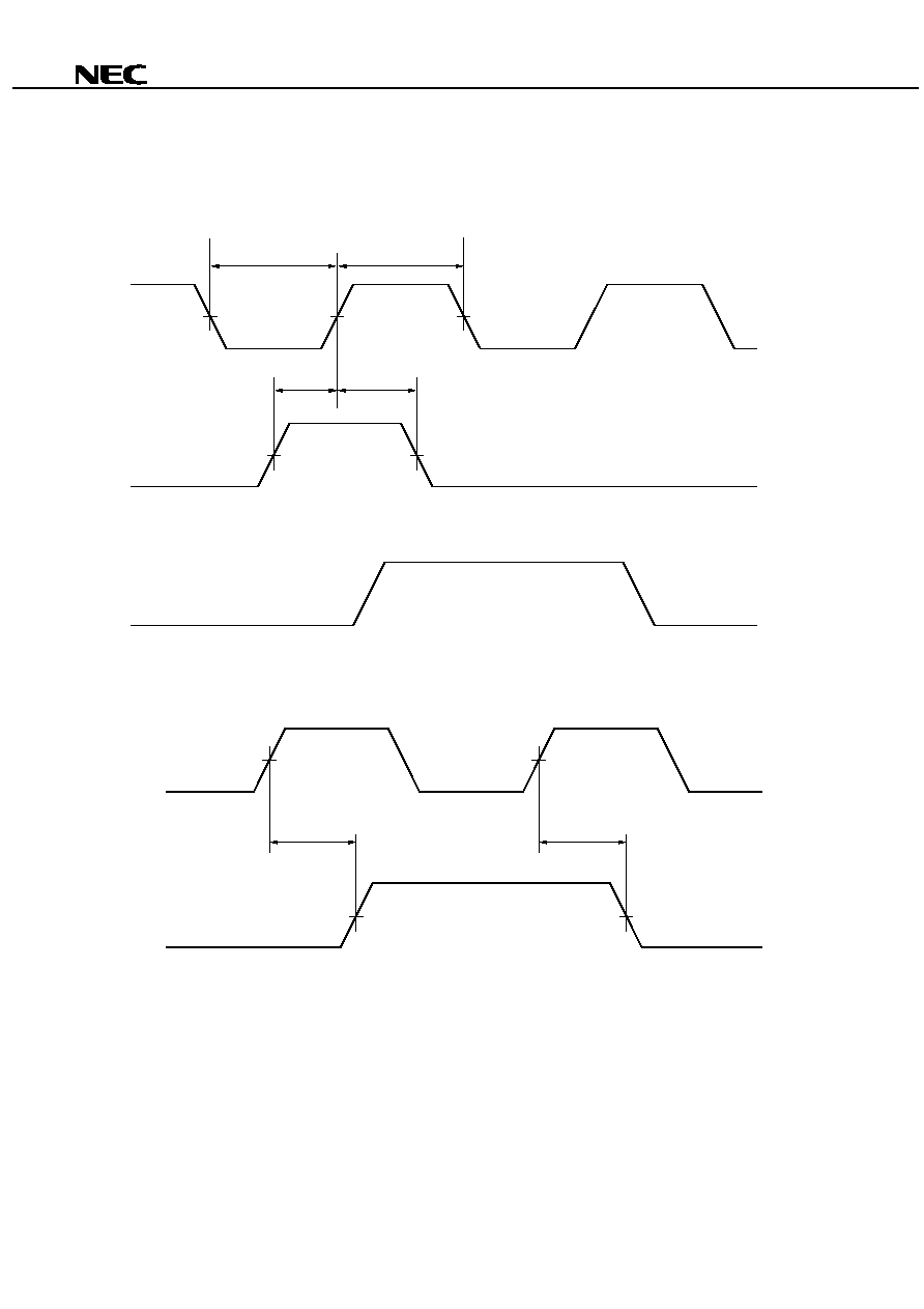
SWITCHING CHARACTERISTIC WAVE (simultaneous/successive sampling)
Start Pulse Input Timing
Start Pulse Output Timing
CLI
1
V
DD1
V
SS1
STHL
(STHR)
V
OH
V
OL
50 %
50 %
t
PLH
50 %
50 %
t
PHL
Remark The input/output timing of the start pulse is the same for simultaneous/successive sampling.
CLI
1
V
DD1
V
SS1
STHR
(STHL)
V
DD1
V
SS1
SHP
1
(SHP
240
)
V
DD1
V
SS1
50 %
50 %
PW
CLI1
PW
CLI1
50 %
50 %
t
SETUP
t
HOLD

21
µ
µ
µ
µ
PD16448A
RESET INH Pulse Timing
CLI
1
RESET
INH
PW
RES
t
ISETUP
t
IIHOLD
PW
INH
t
R-I
50%
50%
50%
50%
50%
5

22
µ
µ
µ
µ
PD16448A
4. RECOMMENDED CONDITIONS FOR INSTALLATION
This product should be installed under the following recommended conditions. Consult one of our sales
representatives for installation under conditions other than those recommended.
Installation Condition
Installation Method
Condition
Soldering
Heat with heating tool at 300
∞
C to 350
∞
C under pressure of 100 g
(per pin) for 2 to 3 seconds
Thermocompression
bonding
ACF (sheet type adhesive agent)
Temporary adhesion at 70
∞
C to 100
∞
C under pressure of 3 to
8 kg/cm
2
for 3 to 5 seconds
Permanent adhesion at 165
∞
C to 180
∞
C under pressure of 25 to
45 kg/cm
2
for 30 to 40 seconds
(when aeolotropic conductive film SUMIZAC 1003 from Sumitomo
Bakelite Co., Ltd. is used)
Caution For installation conditions for the ACF part, contact the ACF manufacturer beforehand. Do not mix
different installation methods.
23
µ
µ
µ
µ
PD16448A
NOTES FOR CMOS DEVICES
1
PRECAUTION AGAINST ESD FOR SEMICONDUCTORS
Note: Strong electric field, when exposed to a MOS device, can cause destruction
of the gate oxide and ultimately degrade the device operation. Steps must
be taken to stop generation of static electricity as much as possible, and
quickly dissipate it once, when it has occurred. Environmental control must
be adequate. When it is dry, humidifier should be used. It is recommended
to avoid using insulators that easily build static electricity. Semiconductor
devices must be stored and transported in an anti-static container, static
shielding bag or conductive material. All test and measurement tools
including work bench and floor should be grounded. The operator should
be grounded using wrist strap. Semiconductor devices must not be touched
with bare hands. Similar precautions need to be taken for PW boards with
semiconductor devices on it.
2
HANDLING OF UNUSED INPUT PINS FOR CMOS
Note: No connection for CMOS device inputs can be cause of malfunction. If no
connection is provided to the input pins, it is possible that an internal input
level may be generated due to noise, etc., hence causing malfunction. CMOS
devices behave differently than Bipolar or NMOS devices. Input levels of
CMOS devices must be fixed high or low by using a pull-up or pull-down
circuitry. Each unused pin should be connected to V
DD
or GND with a
resistor, if it is considered to have a possibility of being an output pin. All
handling related to the unused pins must be judged device by device and
related specifications governing the devices.
3
STATUS BEFORE INITIALIZATION OF MOS DEVICES
Note: Power-on does not necessarily define initial status of MOS device. Production
process of MOS does not define the initial operation status of the device.
Immediately after the power source is turned ON, the devices with reset
function have not yet been initialized. Hence, power-on does not guarantee
out-pin levels, I/O settings or contents of registers. Device is not initialized
until the reset signal is received. Reset operation must be executed imme-
diately after power-on for devices having reset function.

µ
µ
µ
µ
PD16448A
REFERENCE
NEC Semiconductor Device Reliability/Quality Control System
Quality Grade on NEC Semiconductor Devices
C10983E
C11531E
No part of this document may be copied or reproduced in any form or by any means without the prior written
consent of NEC Corporation. NEC Corporation assumes no responsibility for any errors which may appear in this
document.
NEC Corporation does not assume any liability for infringement of patents, copyrights or other intellectual
property rights of third parties by or arising from use of a device described herein or any other liability arising
from use of such device. No license, either express, implied or otherwise, is granted under any patents,
copyrights or other intellectual property rights of NEC Corporation or others.
While NEC Corporation has been making continuous effort to enhance the reliability of its semiconductor devices,
the possibility of defects cannot be eliminated entirely. To minimize risks of damage or injury to persons or
property arising from a defect in an NEC semiconductor device, customers must incorporate sufficient safety
measures in its design, such as redundancy, fire-containment, and anti-failure features.
NEC devices are classified into the following three quality grades:
"Standard", "Special", and "Specific". The Specific quality grade applies only to devices developed based on
a customer designated "quality assurance program" for a specific application. The recommended applications
of a device depend on its quality grade, as indicated below. Customers must check the quality grade of each
device before using it in a particular application.
Standard: Computers, office equipment, communications equipment, test and measurement equipment,
audio and visual equipment, home electronic appliances, machine tools, personal electronic
equipment and industrial robots
Special: Transportation equipment (automobiles, trains, ships, etc.), traffic control systems, anti-disaster
systems, anti-crime systems, safety equipment and medical equipment (not specifically designed
for life support)
Specific: Aircrafts, aerospace equipment, submersible repeaters, nuclear reactor control systems, life
support systems or medical equipment for life support, etc.
The quality grade of NEC devices is "Standard" unless otherwise specified in NEC's Data Sheets or Data Books.
If customers intend to use NEC devices for applications other than those specified for Standard quality grade,
they should contact an NEC sales representative in advance.
Anti-radioactive design is not implemented in this product.
M4 96. 5
The application circuits and their parameters are for reference only and are not intended for use in actual design-ins.