Document Outline
- COVER
- FEATURES
- ORDERING INFORMATION
- BLOCK DIAGRAM
- PIN CONFIGURATION (Top View)
- ABSOLUTE MAXIMUM RATING (TA = 25∞C unless otherwise specified)
- ELECTRICAL CHARACTERISTICS (Tch = 25∞C unless otherwise specified)
- TYPICAL CHARACTERISTICS
- APPLICATION CIRCUIT EXAMPLE
- RECOMMENDED SOLDERING CONDITIONS
N-CHANNEL LOW SIDE INTELLIGENT POWER DEVICE
The information in this document is subject to change without notice. Before using this document, please
confirm that this is the latest version.
Not all products and/or types are available in every country. Please check with an NEC Electronics
sales representative for availability and additional information.
2005
Document No. S17476EJ1V0DS00 (1st edition)
Date Published March 2005 NS CP (K)
Printed in Japan
µ
PD166100, 166101
MOS INTEGRATED CIRCUIT
DATA
SHEET
The
µ
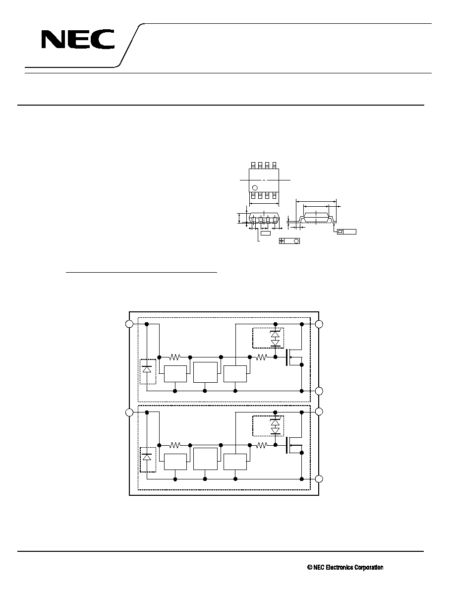
PD166100, 166101 are N-channel Low-side Driver for Solenoids and Lamp Drivers. It build in protection functions.
FEATURES
Built in current limit and thermal shutdown circuit.
Thermal shutdown will automatically restart after
the channel temperature has cool down.
Low on-state resistance: R
DS(ON)
= 160 m
(V
IN
= 5 V, I
OUT
= 0.8 A, T
ch
= 25
∞C)
Built in dynamic clamp circuit
µ
PD166101: Dual channel Low-side switch
Small and surface mount package
(8-pin SOP)
PACKAGE DRAWING (unit: mm)
1.27
0.12 M
6.0 ±0.3
4.4
0.40
+0.10
≠0.05
0.78 Max.
0.05 Min.
1.8 Max.
1.44
0.8
0.5 ±0.2
0.15
+0.10
≠0.05
5.37 Max.
0.10
1
4
8
5
ORDERING INFORMATION
Part Number
Package
µPD166100GR(20) 8-pin
SOP
µPD166101GR(20) 8-pin
SOP
BLOCK DIAGRAM
IN1
OUT1
GND1
Over
Temperature
Protection
Circuit
Control
Circuit
Current
Limit
IN2
OUT2
GND2
Ch2
Ch1
Dynamic
Clamp
ESD
Control
Circuit
Current
Limit
Dynamic
Clamp
ESD
Over
Temperature
Protection
Circuit
Remark
µ
PD166100: Ch1 only
Data Sheet S17476EJ1V0DS
2
µ
PD166100, 166101
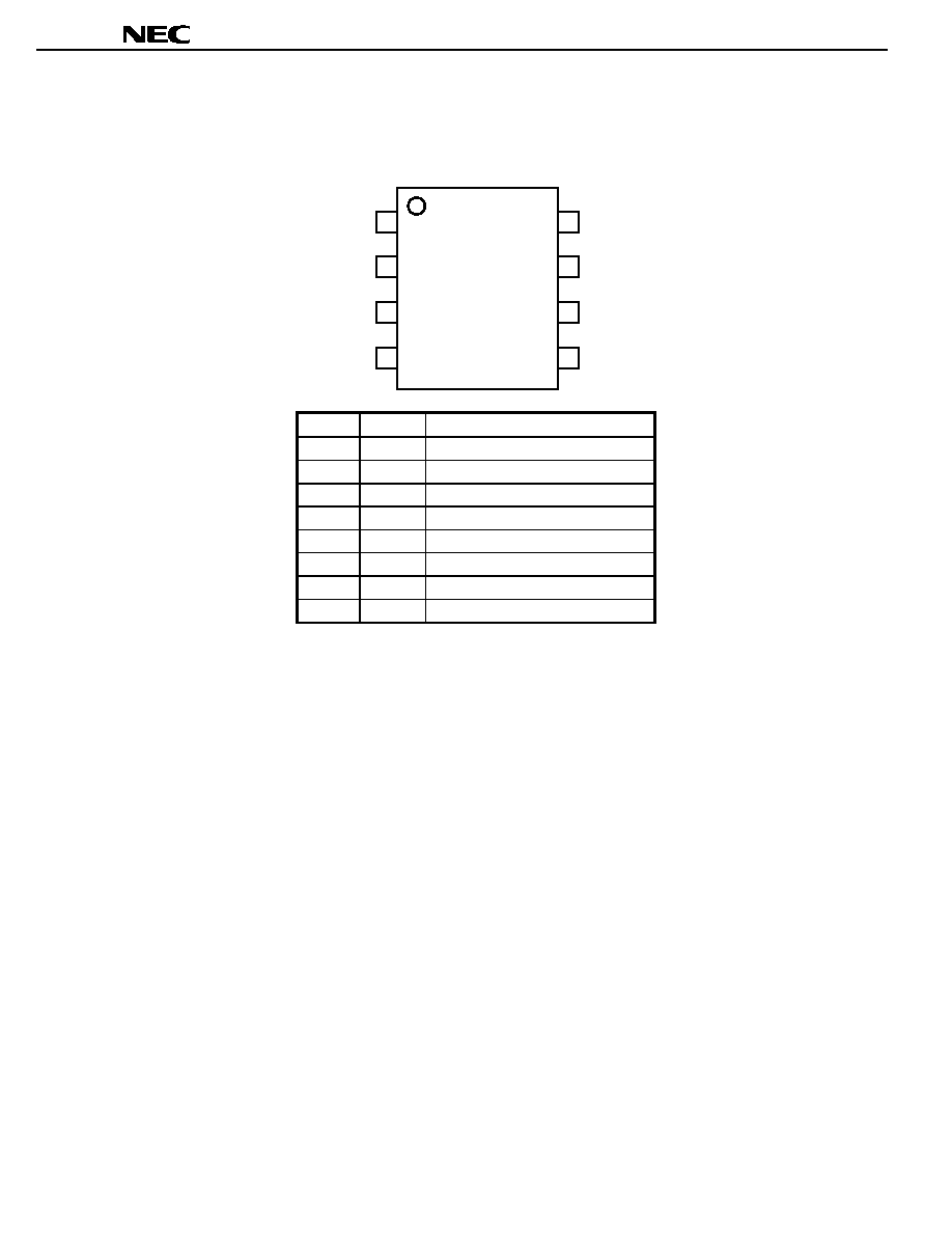
PIN CONFIGURATION (Top View)
∑ 8-pin
SOP
µ
PD166100GR (20),
µ
PD166101GR (20)
1
2
3
4
8
7
6
5
GND1
IN1
GND2
Note
IN2
Note
OUT1
OUT1
OUT2
Note
OUT2
Note
Pin No.
Symbol
Function
1
GND1
Connected to Ground
2
IN1
Input terminal1 (active level is high)
3
GND2
Note
Connected to Ground
4
IN2
Note
Input terminal2 (active level is high)
5
OUT2
Note
Output terminal2
6
OUT2
Note
Output terminal2
7 OUT1 Output
terminal1
8 OUT1 Output
terminal1
Note
µ
PD166100: Pin No.3 to 6 are N.C.
Data Sheet S17476EJ1V0DS
3
µ
PD166100, 166101
ABSOLUTE MAXIMUM RATING (T
A
= 25
∞C unless otherwise specified)
Parameter Symbol
Conditions
Rating Unit
Output voltage
V
OUT
V
IN
= 0 V, DC
40
V
Input voltage
V
IN
7
V
Negative input current
I
IL
-10 mA
Output current
I
OUT(DC)
V
IN
= 5 V
SELF LIMITED
A/UNIT
µPD166100 On-State
1.5
Total power dissipation
P
D
Note
µPD166101 2ch
On-State
2
W
Channel temperature
T
ch
150
∞C
Storage temperature
T
stg
-55 to +150
∞C
Note Mounted on ceramic substrate of 20cm x 20cm x 1.1mm
ELECTRICAL CHARACTERISTICS
(T
ch
= 25
∞C
unless otherwise specified)
Parameter Symbol
Conditions
Min.
Typ.
Max.
Unit
Output clamping voltage
V
OUT
I
OUT
= 1 mA, V
IN
= 0 V
40
60
V
Output Off leakage current
I
OL
V
IN
= V
IL
, V
OUT
= 18 V
100
µA
High Level Input current
I
IH
V
IN
= 5.5 V, V
OUT
= 0 V
300
µA
Low Level Input current
I
IL
V
IN
= 0 V, V
OUT
= 18 V
-10 10
µA
High Level Input voltage
V
IH
I
OUT
= 0.8 A, V
OUT
= 0.2 V
3
V
Low Level Input voltage
V
IL
V
OUT
= 10 V, I
OUT
= 1 mA
1.5
V
V
IN
= 5 V, I
OUT
= 0.8 A
160
m
ON-state resistance
R
DS(ON)
V
IN
= 3 V, I
OUT
= 0.8 A
195
m
Turn-on time
t
on
120
µs
Rise time
t
r
80
µs
Turn-off time
t
off
200
µs
Fall time
t
f
V
CC
= 18 V, R
L
= 22
,
V
IN
= 0 V to 5 V,
R
IN
= 10
80
µs
Thermal shutdown
detection temperature
Note
T
HI
V
IN
= 5 V
150
∞C
Current limit
I
S
V
IN
= 3 V
1
A
Input frequency
f
IN
1
kHz
Note The low side switch is shutdown if the channel temperature exceeds thermal shutdown temperature.
It will automatically restart after the channel temperature has cooled down than thermal shutdown temperature.
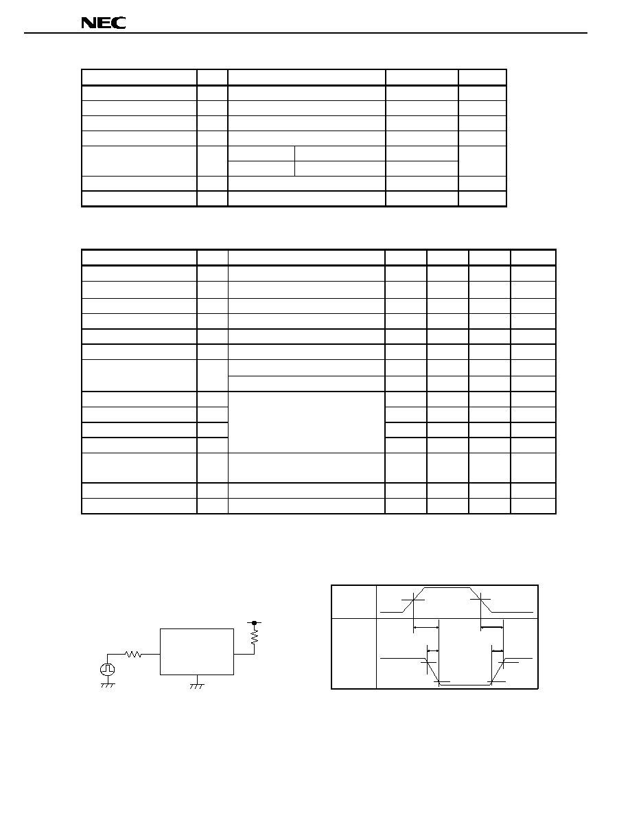
TEST CIRCUIT
V
C C
= 18 V
R
L
= 22
V
IN
IN
O U T
G N D
µPD 166100,
µPD166101
IN
Wave Form
OUT
Wave Form
90%
50%
90%
10%
50%
10%
t
on
t
r
t
off
t
f

Data Sheet S17476EJ1V0DS
4
µ
PD166100, 166101
TYPICAL CHARACTERISTICS
TOTAL POWER DISSIPATION vs.
AMBIENT TEMPERATURE
0
0.4
0.8
1.2
1.6
2
2.4
2.8
0 20 40 60 80 100
1
20
140
160
T
A
- Ambient Temperature -
∞C
P
T
- T
o
t
a
l
P
o
we
r
Di
s
s
i
p
at
ion ≠
W
/
p
ac
ka
g
e
Mounted on ceramic
substrate of
2000 mm
2
x 2.25 mm
1 unit
2 unit
OUTPUT OFF LEAKAGE CURRENT vs.
AMBIENT TEMPERATURE
0
10
20
30
40
50
60
70
80
90
100
-50
0
50
100 150 200
T
A
- Ambient Temperature -
∞C
I
OL
-
Out
p
u
t Off L
e
a
kage
Cu
rrent
-
µ
A
V
IN
= V
IL
, V
OUT
= 18 V
HIGH LEVEL INPUT CURRENT vs.
INPUT VOLTAGE
0
100
200
300
400
500
0
3 4 5 6 7
V
IN
- Input Voltage - V
I
IH
- Hi
gh
Lev
e
l Inp
u
t
C
u
r
r
e
nt
-
µ
A
1 2
8
V
OUT
= 0 V
600
T
A
= 25
∞C
T
A
=
-40∞C
T
A
= 85
∞C
T
A
= 105
∞C
HIGH LEVEL INPUT CURRENT vs.
AMBIENT TEMPERATURE
0
50
100
150
200
250
300
350
400
-50
0
50
100 150 200
T
A
- Ambient Temperature -
∞C
I
IH
-
Hi
gh
Le
vel I
npu
t C
u
r
r
e
nt
-
µ
A
V
IN
= 5.5 V, V
OUT
= 0 V
HIGH LEVEL INPUT VOLTAGE vs.
AMBIENT TEMPERATURE
0.0
0.5
1.0
1.5
2.0
2.5
3.0
3.5
4.0
-50
0 50
100
150
200
T
A
- Ambient Temperature -
∞C
V
IH
-
High Lev
e
l Input
V
o
l
t
age
- V
I
OUT
= 0.8 A
LOW LEVEL INPUT VOLTAGE vs.
AMBIENT TEMPERATURE
0.0
0.5
1.0
1.5
2.0
2.5
3.0
-50
0
50
100 150 200
T
A
- Ambient Temperature -
∞C
V
IL
- Lo
w Le
ve
l
I
npu
t V
ol
t
a
ge
-
V
I
OUT
= 1 mA
Data Sheet S17476EJ1V0DS
5
µ
PD166100, 166101
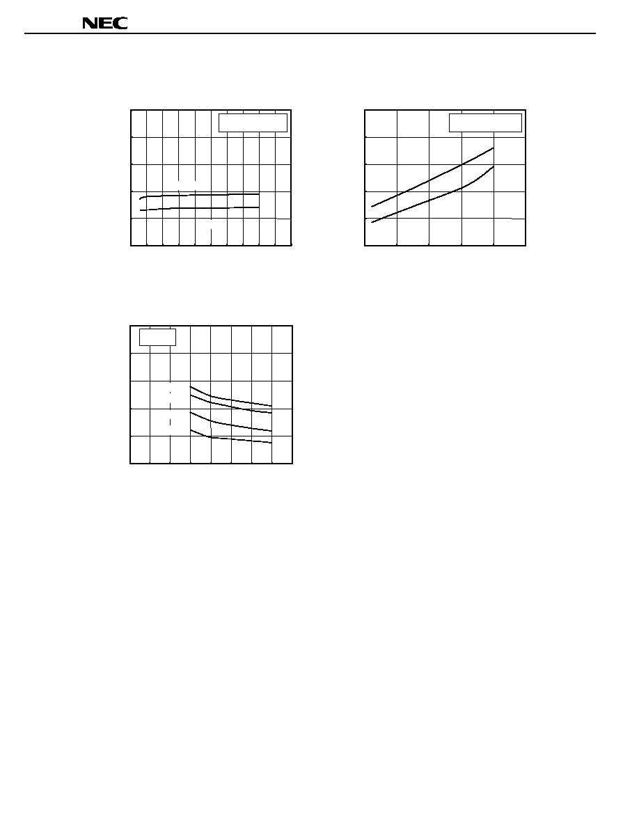
ON-STATE RESISTANCE vs.
OUTPUT CURRENT
0
0.05
0.1
0.15
0.2
0.25
0 0.1 0.2
I
OUT
- Output Current - A
R
DS
(ON
)
-
O
N
-
S
t
ate
Re
si
s
t
an
ce
-
0.3 0.4 0.5 0.6 0.7 0.8 0.9
1
V
IN
= 3 V, 5 V, T
A
= 25
∞C
V
IN
= 5 V
V
IN
= 3 V
ON-STATE RESISTANCE vs.
AMBIENT TEMPERATURE
-50
0
50
100 150 200
T
A
- Ambient Temperature -
∞C
R
DS(O
N)
-
ON-
S
t
a
t
e
Re
si
s
t
an
ce
-
V
IN
= 3 V, 5 V, I
OUT
= 0.8 A
V
IN
= 5 V
V
IN
= 3 V
0
0.05
0.1
0.15
0.2
0.25
ON-STATE RESISTANCE vs.
INPUT VOLTAGE
0
3 4 5 6
8
V
IN
- Input Voltage - V
0
0.05
0.1
0.15
0.2
0.25
R
DS(O
N
)
-
O
N
-
S
t
ate
Re
si
s
t
an
c
e -
1 2
7
I
OUT
= 0.8 A
T
A
= 25
∞C
T
A
=
-40∞C
T
A
= 85
∞C
T
A
= 105
∞C